

Page 1
Preliminary
RT9268
Tiny Package, 1.3MHz, Step-up DC/DC Converter
General Description
The RT9268 is a compact, 1.3MHz, step-up DC/DC
converter with a current mode PWM control loop,
providing a stable and ef ficient operation without external
compensation.
The high switching frequency makes RT9268 suitable
for ADSL applications providing sufficient output current
for variant types of line drivers. This device is available
in space-saving SOT -23-6 package.
The output voltage is set with 2 external resistors. Both
internal 2A switch and driver for driving external power
devices (NMOS or NPN) are provided.
Ordering Information
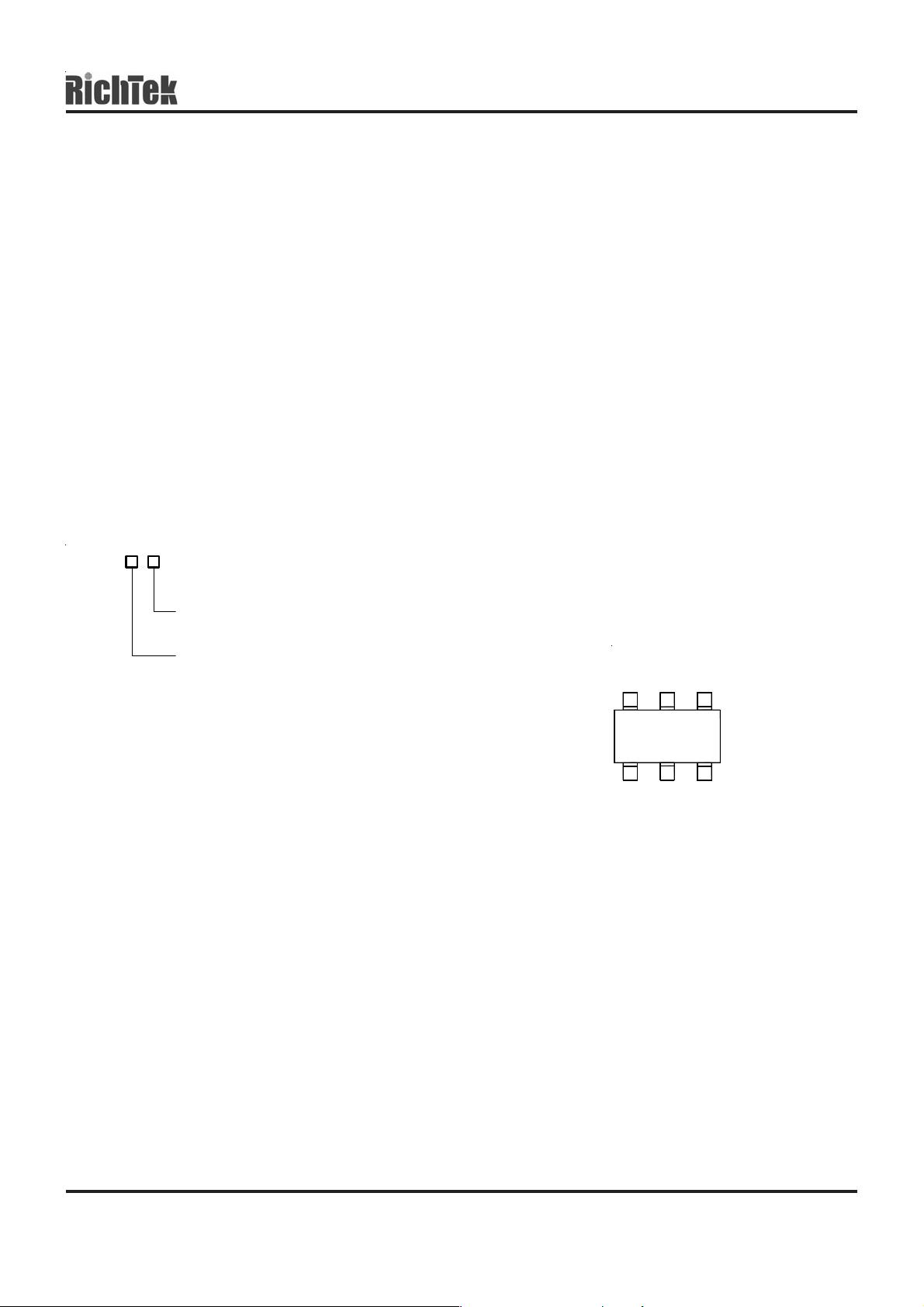
RT9268
Package Type
E : SOT-23-6
Operating Temperature Range
C : Commercial Standard
P : Pb Free with Commercial Standard
Note :
RichTek Pb-free products are :
−RoHS compliant and compatible with the current require ments of IPC/JEDEC J-STD-020.
−Suitable for use in SnPb or Pb-free soldering processes.
−100%matte tin (Sn) plating.
Marking Information
Features
zz
1.3MHz Switching Frequency
z
zz
zz
z Below 2V Low Start-up Input Voltage
zz
zz
z Sufficient Supply Capability for Supplying XDSL
zz
Line Drivers
zz
z Zero Shutdown Mode Supply Current
zz
zz
z Providing Flexibility for Using Internal and Extern al
zz
Power Switches
z Small SOT-23-6 Package
zz
z RoHS Compliant and 100% Lead (Pb)-Free
zz
Applications
z XDSL Line Drivers
z USB Devices
z PCMCIA Cards
z Mini-PCI Cards
Pin Configurations
(TOP VIEW)
FB VDD
1
EN
SOT-23-6
Note : There is no pin1 indicator on top mark for SOT-23-6
type, and pin 1 will be lower left pin when reading top mark
from left to right.
LX
4
56
23
GND
EXT
For marking information, contact our sales re presentative
directly or through a RichTek distributor located in your
area, otherwise visit our website for detail.
DS9268-06 March 2005 www.richtek.com
1
Page 2
RT9268
Typical Application Circuit
V
IN
0.3V to 5.5V
C1
1uF
VDD
EN
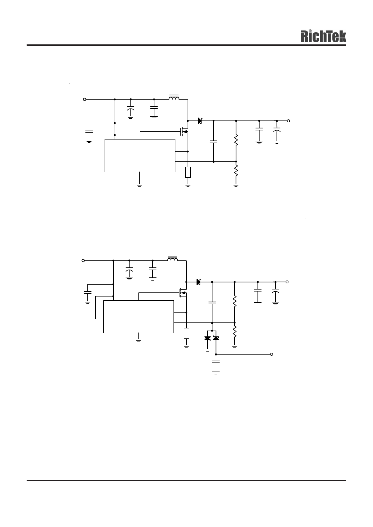
Figure 1. RT9268 Application for XDSL 18V Line Drivers
C2
10uF
RT9268
GND
Preliminary
L1
3.3uF
C3
1uF
EXT
LX
FB
L2 : CL321611T-R22K-S/ YAGEO
D1
Q1
N MOS
L2
C4
0.1uF
R1
12k
R2
910
C5
1uF
+
C6
10uF
V
18V
OUT
V
IN
4.5V to 5.2V
C1
1uF
L1
3.3uF
VDD
EN
C2
10uF
EXT
RT9268
GND
C3
1uF
LX
FB
D1
Q1
N MOS
L2
D2
C4
0.1uF
D3
C8
10uF
R1
8.6K
R2
1k
C5
1uF
L2 : CL321611T-R22K-S/ YAGEO
Figure 2. RT9268 Application for USB-XDSL ±12V Line Drivers
+
V
OUT2
-12V
C6
10uF
V
12V
OUT1
DS9268-06 March 2005www.richtek.com
2
Page 3
Functional Pin Description
Preliminary
RT9268
Pin No. Pin Name
1 EN
2 EXT
3 GND
4 LX
5 VDD
6 FB
Pin Function
Chip Enable (Active High)
Output Pin for Driving External NMOS
Ground
Pin for Switching
Input Positive Power Pin of RT9268
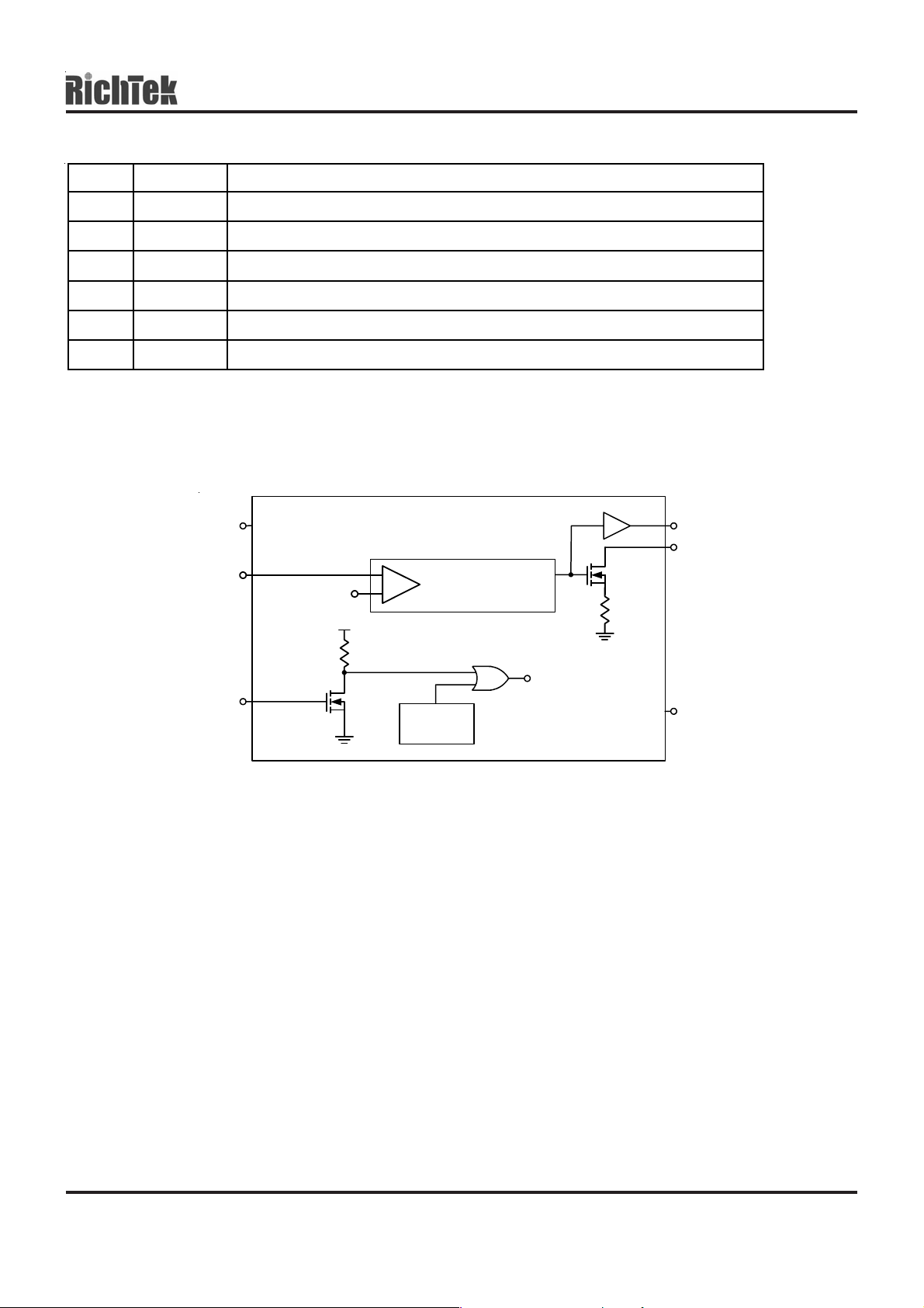
Feedback Input Pin Internal refe rence voltage for the error amplifie r is 1.25V.
Function Block Diagram
VDD
FB
1.25V
VDD
-
Loop Control Circuit
+
RT9268
EXT
LX
Q1
N MOS
R1
EN
R2
Q2
N MOS
Over Temp.
Detector
Shut Down
GND
DS9268-06 March 2005 www.richtek.com
3
Page 4
RT9268
Preliminary
Absolute Maximum Ratings
z Supply V oltage-----------------------------------------------------------------------------------------------------−0.3V to 7V
z LX Pin Switch Voltage--------------------------------------------------------------------------------------------−0.3V to (V
z Other I/O Pin Voltages -------------------------------------------------------------------------------------------−0.3V to (V
z LX Pin Switch Current --------------------------------------------------------------------------------------------2.5A
z EXT Pin Driver Current --------------------------------------------------------------------------------------------200mA
z Power Dissipation, P
@ TA = 25°C
D
+ 0.8V)
DD
+ 0.3V)
DD
SOT-23-6 ------------------------------------------------------------------------------------------------------------0. 25W
z Package Thermal Resista nce
SOT-23-6, θJA-------------------------------------------------------------------------------------------------------250°C/W
z Operating Junction T emperature ------------------------------------------------------------------------------- 125°C
z Storage T emperature Range ------------------------------------------------------------------------------------ −65°C to +150°C
Electrical Characteristics
(V
= 3.3V, V
IN
set to 5V, Load Current = 0, T
DD
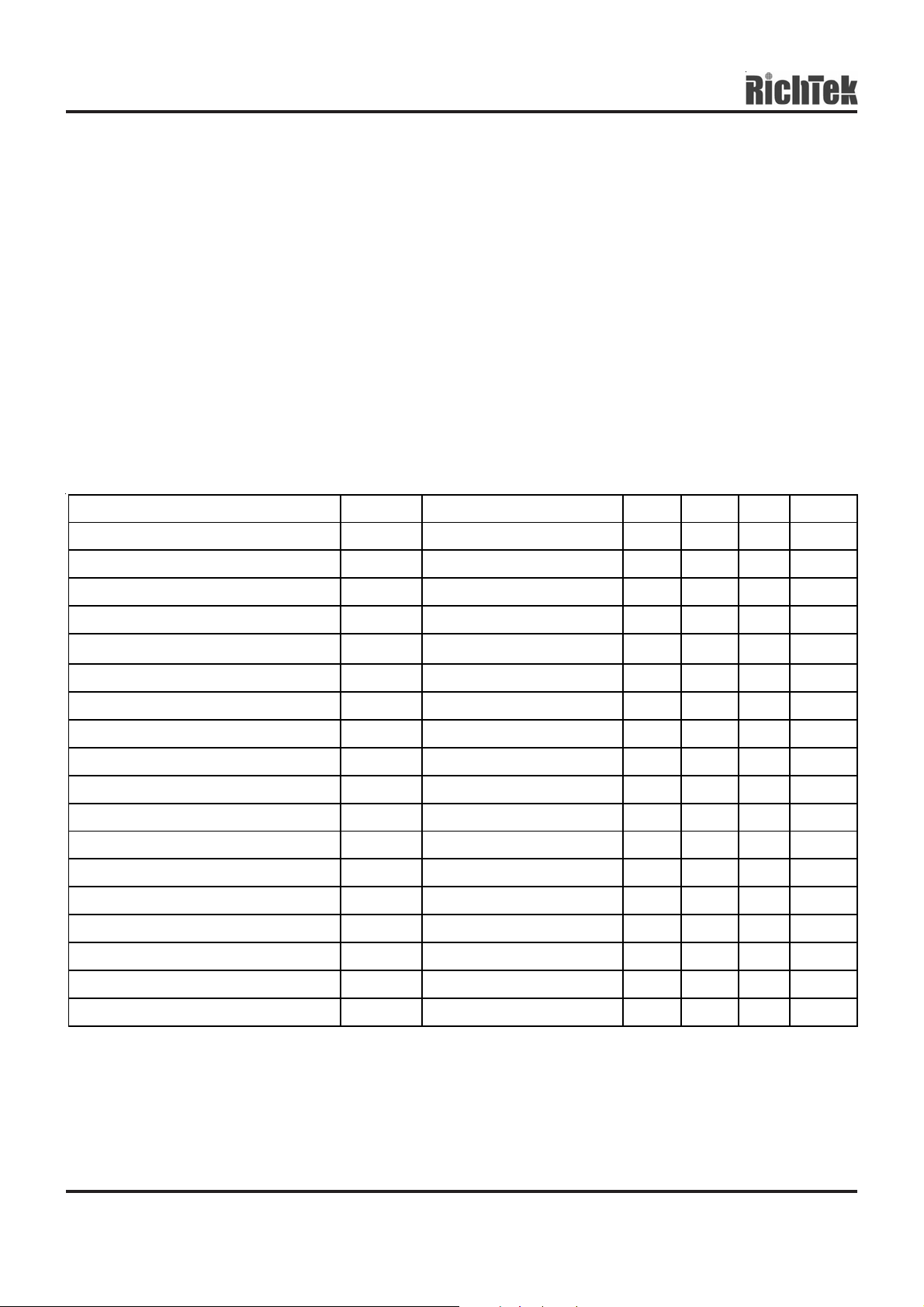
Parameter Symbol Test Conditions Min Typ Max Units
= 25°C, unless otherwise specified)
A
Start-U P Vol tage
Operating VDD Range
No Load Current I (VIN) I
Switch-off Current I (VDD)
Shutdown Current I (VIN) I
Feedback Reference Voltage
Switching Frequency
Maximum Duty
LX ON Resistance
Current Limit Setting
EXT ON Resistance to
V
DD
EXT ON Resistance to GND
Line Regulation
Load Regulation
EN Pin Trip Level
Temperature Stability for Vout
Thermal Shutdown
Thermal Shutdown Hysterises
V
I
ST
V
DD
NO LOAD
I
SWITCH
EN Pin = 0V, VIN = 6V
OFF
V
REF
F
S
D
MAX
I
LIMIT
∆V
LINE
∆V
LOAD
T
s
T
SD
∆T
SD
= 1mA
L
pin voltage
V
DD
VIN = 3.3V, V
VIN = 6V
= 5V
V
DD
= 5V
V
DD
V
= 5V
DD
= 5V
V
DD
= 5V
V
DD
V
= 5V
DD
V
VIN = 3.3V, I
= 2 ~ 4V, I
IN
V
= 5V
DD
L
Guaranteed by Design -- 50 -Guaranteed by Design -- 165 -Guaranteed by Design -- 10 --
= 5V
OUT
= 1mA
L
= 1 ~ 100mA
-- -- 2 V
2 -- 6.5 V
-- 3 -- mA
-- 1 -- mA
-- 0.1 1
µA
1.225 1.25 1.275 V
-- 1.3 -- MHz
-- 95 -- %
-- 0.3 --
-- 2 --
-- 5 --
-- 5 --
-- 10 --
-- 0.25 --
Ω
A
Ω
Ω
mV/V
mV/mA
0.4 0.8 1.2 V
ppm/°C
°C
°C
* Note. The EN pin shall be tied to VDD pin and inhibit to act the ON/OFF state whenever the VDD pin voltage may reach to 5.5V
or above.
DS9268-06 March 2005www.richtek.com
4
Page 5
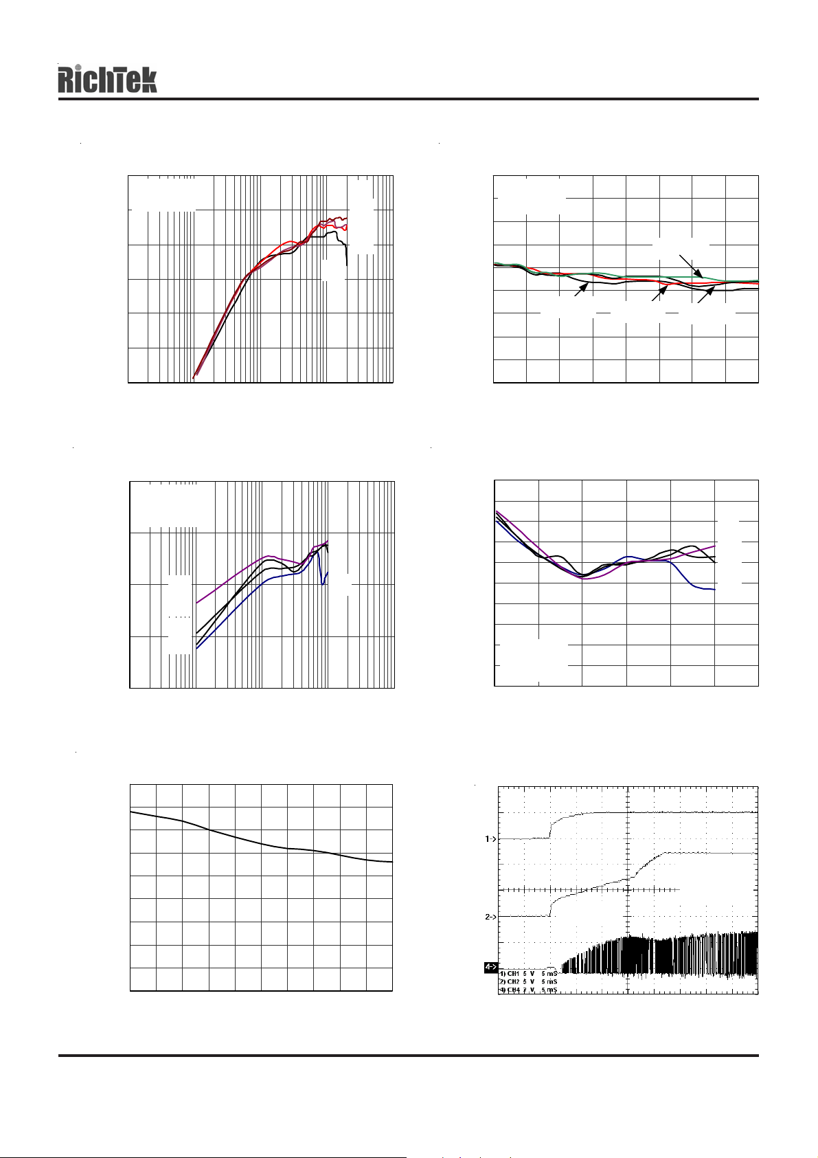
Typical Operating Characteristics
Preliminary
RT9268
Efficiency vs.Output Current
100
V
= 12V
OUT
T
= 25°C
A
90
80
70
60
Efficiency (%)
50
40
0.1 1 10 100 1000
4.5V
Output Currrent (mA)
Efficiency vs. Output Current
90
V
= 18V
OUT
TA = 25°C
80
70
V
IN
5.5V
Efficiency (%)
60
50
0.1 1 10 100 1000
5.0V
5.2V
Output Current (mA)
4.5V
V
5.5V
5.2V
5.5V
Output Voltage vs. Output Current
12.5
V
= 12V
OUT
IN
12.4
12.3
12.2
12.1
12
11.9
Output Voltage (V)
11.8
11.7
11.6
T
= 25°C
A
V
= 5.5V
IN
V
= 5.5V
IN
0 25 50 75 100 125 1 50 175 200
V
= 5.5V
IN
V
IN
= 5.5V
Output Current (mA)
Output Voltage vs. Output current
17.8
17.78
17.76
17.74
17.72
17.7
17.68
17.66
Output Voltage (V)
17.64
V
= 18V
OUT
17.62
17.6
TA = 25°C
0 20 40 60 80 100 120
Output Current (mA)
V
IN
5.5V
5.0V
5.2V
4.5V
Input Current vs. Input Voltage
0.9
0.8
0.7
0.6
0.5
0.4
0.3
Input Current (mA)
0.2
0.1
0
4.5 4.6 4.7 4.8 4.9 5 5.1 5.2 5.3 5.4 5.5
Input Vol tage (V)
V
LX
IN
Start - up Waveform
= 5V
V
= 12V
OUT
Time (5ms/Div)
I
= 200mA
OUT
TA = 25°C
DS9268-06 March 2005 www.richtek.com
5
Page 6
RT9268
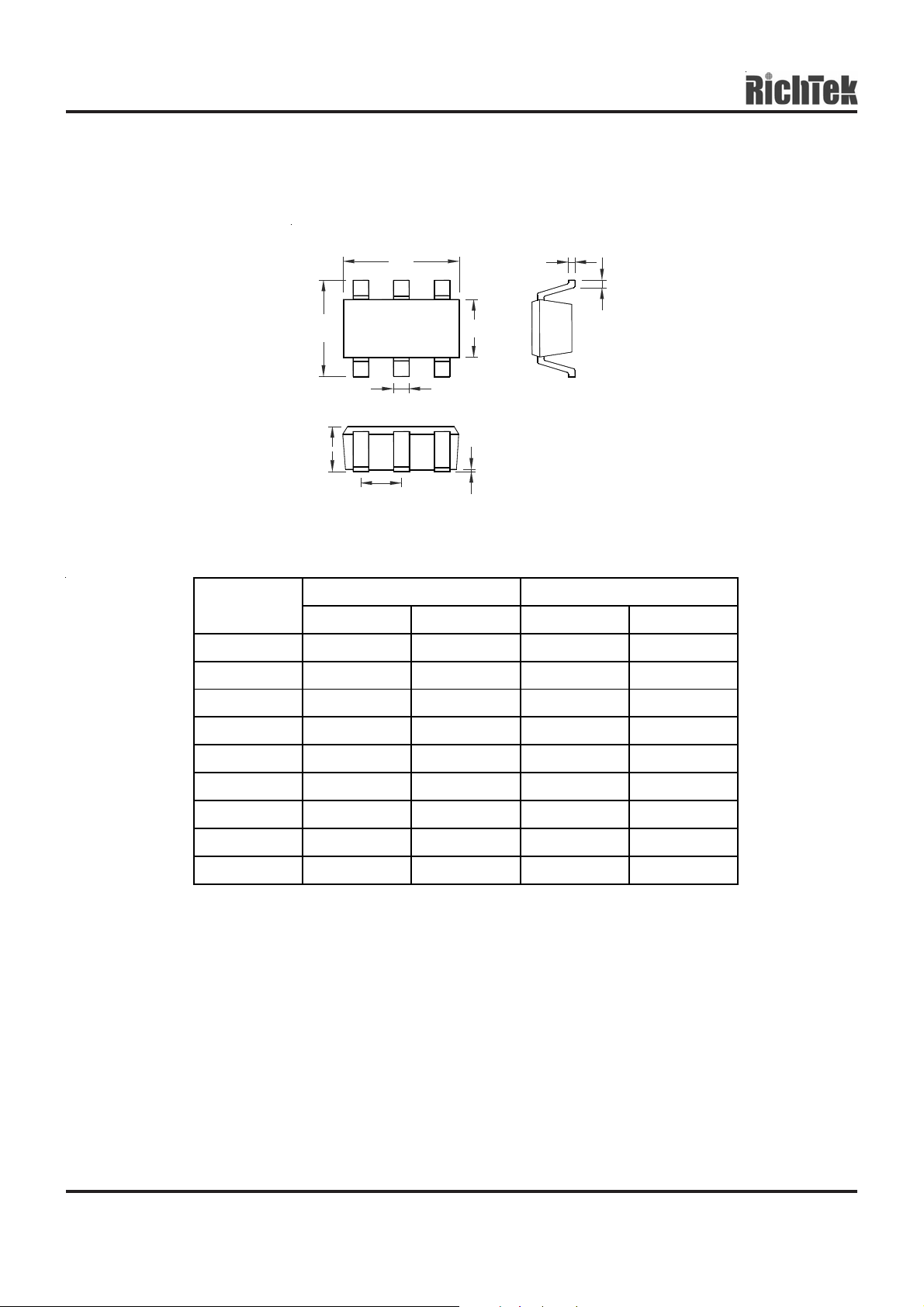
Outline Dimension
Preliminary
H
D
L
C
b
A
e
Dimensions In Millimeters Dimensions In Inches
Symbol
Min Max Min Max
A 0.889 1.295 0.031 0.051
A1 0.000 0.152 0.000 0.006
B 1.397 1.803 0.055 0.071
b 0.250 0.560 0.010 0.022
C 2.591 2.997 0.102 0.118
B
A1
D 2.692 3.099 0.106 0.122
e 0.838 1.041 0.033 0.041
H 0.080 0.254 0.003 0.010
L 0.300 0.610 0.012 0.024
RICHTEK TECHNOLOGY CORP.
Headquarter
5F, No. 20, Taiyuen Street, Chupei City
Hsinchu, Taiwan, R.O.C.
Tel: (8863)5526789 Fax: (8863)5526611
6
SOT-23-6 Surface Mount Package
RICHTEK TECHNOLOGY CORP.
Taipei Office (Marketing)
8F-1, No. 137, Lane 235, Paochiao Road, Hsintien City
Taipei County, Taiwan, R.O.C.
Tel: (8862)89191466 Fax: (8862)89191465
Email: [email protected]
DS9268-06 March 2005www.richtek.com
Page 7

 Loading...