

®
RT9526A
Linear Single Cell Li-Ion Battery Charger with Input Over
Voltage Protection
General Description
The RT9526A is a fully integrated low cost single cell Liion battery charger ideal for portable applications. The
RT9526A is capa ble of being powered up from AC ada pter
and USB (U niversal Serial Bus) port inputs. The RT9526A
enters sleep mode when supplies are removed. The
RT9526A opti mizes the charging task by using a control
algorithm including preconditioning mode, fast charge
mode, and consta nt voltage mode. The charging ta sk will
remain in constant voltage mode to hold the battery in a
full charge condition. The charge current can be
programmed with a n external resistor . The internal thermal
feedback circuitry regulates the die temperature to opti mize
the charge rate under all ambient temperatures. The
RT9526A features 28V maximum rating voltage for VIN.
Under-voltage protection a nd over-voltage protection are
provided for the AC a da pter supply.
The RT9526A is available in the WDFN-8L 2x3 and
SOT-23-6 pa ckage to achieve be st solution for PCB space
and total BOM cost saving considerations.
Applications
Cellular Phones
Digital Camera s
PDAs and Smart Phones
Portable Instruments
Features
28V Maximum Rating for AC Adapter with Over-
Voltage Protection 7V
Internal Integrated Power FETs
AC Adapter Power Good Status Indicator
Programmed Charging Current
Charge Status Indicator
Programmed End of Charge Current
Under-Voltage Protection
Thermal Feedback Optimizing Charge Rate
RoHS Compliant and Halogen Free
Ordering Information
RT9526A
Package Type
QW : WDFN-8L 2x3 (W-Type)
E : SOT-23-6
Lead Plating System
G : Green (Halogen Free and Pb Free)
Note :
Richtek products are :
RoHS compliant and compatible with the current require-
ments of IPC/JEDEC J-STD-020.
Suitable for use in SnPb or Pb-free soldering processes.
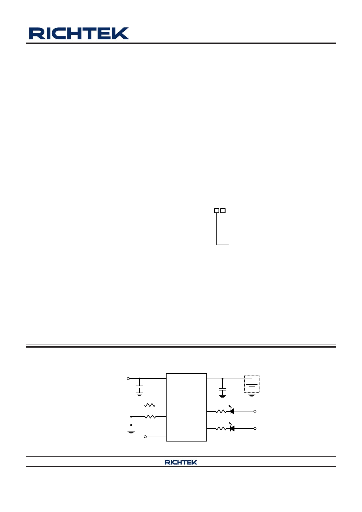
Simplified Application Circuit
Adapter or USB
C
IN
R
ISET
R
IMIN
Copyright 2014 Richtek Technology Corporation. All rights reserved. is a registered trademark of Richtek Technology Corporation.
©
DS9526A-03 July 2014 www.richtek.com
VIN
ISET
IMIN
GND
ENB
RT9526A
CHG_SB
BATT
PGB
R1
R2
C
OUT
V
BATT
V
BATT
1
RT9526A
Marking Information
RT9526AGQW
05 : Product Code
05W
RT9526AGE
0X=DNN
W : Date Code
0X= : Product Code
DNN : Date Code
Function Pin Description
Pin No.
WDFN-8L 2x3 SO T-2 3- 6
1 3 VIN Supply Voltage Input. VIN can withstand up to 28V input.
2 -- PGB
3 1 CHG_SB
4 -- ENB
5,
9 (Exp ose d Pad)
2 GND
6 6 IMIN EOC Current Setting.
7 5 ISET Charge Current Set Point.
8 4 BATT Battery Charge Current Output.
Pin Name Pin Fun ction
Pin Configurations
(TOP VIEW)
1
VIN
2
PGB
CHG_SB
3
4
ENB
WDFN-8L 2x3
IMIN
CHG_SB
SOT-23-6
Po wer Go od In dic ato r . This pin con nec ts to VIN with 10S L N-M O SFE T
as power good condition.
Charge Status Indicator Output (Open-Drain). Indicate low when
bat t ery is charging; indi c ate hi gh wh en ba tte r y char gi ng fi nish ed or an y
fault happened.
Enable Control Input (Active Low). Connect this pin with a 200k
pull-low resistor.
Ground. The exposed pad must be soldered to a large PCB and
connected to GND for maximum power dissipation.
8
7
6
GND
9
5
ISET BATT
4
56
23
VIN
GND
BATT
ISET
IMIN
GND
Copyright 2014 Richtek Technology Corporation. All rights reserved. is a registered trademark of Richtek Technology Corporation.
2
©
DS9526A-03 July 2014www.richtek.com
Function Block Diagram
RT9526A
Switch
Well
Operation
VIN
ISET
ENB
BASE
Sleep
Mode
Current
Set Block
OVP
UVLO
200k
V
I
BIAS
REF
CC/CV/TR
Multi Loop
Controller
Logic
EOC Set
Block
BATT
IMIN
CHG_SB
PGB
GND
The RT9526A is a fully integrated low cost single cell Liion charger. It provides a fast-charge current setting by
resistor R
. Pre-charge is 16.7% of fast charge current,
IREF
while VBAT < 2.45V. The PGB pin is low, while VIN >
POR, VIN < OVP , and VIN − VBA T > V
. The CHG_SB
OSH_H
pin is low, while RT9526A is charging. The CHG_SB pin
will go high while end of charger happen s. End of charge
condition is set by R
. CHG_SB will go low again, while
IMIN
charge current is larger than 75% of fast-charge setting.
The RT9526A charges continuously after end of charge
happen s. Li-ion battery will be full charged until CV = 4.2V .
The RT9526A ca n be disa bled by ENB = H.
Copyright 2014 Richtek Technology Corporation. All rights reserved. is a registered trademark of Richtek Technology Corporation.
©
DS9526A-03 July 2014 www.richtek.com
3
RT9526A
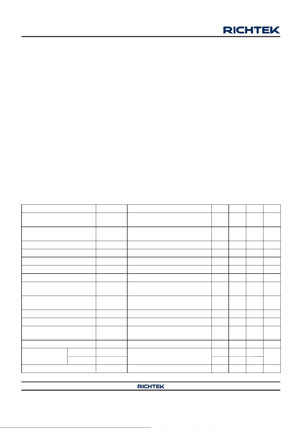
Absolute Maximum Ratings (Note 1)
Supply V oltage, VIN ------------------------------------------------------------------------------------------------------ −0.3V to 28V
CHG_SB, PGB ------------------------------------------------------------------------------------------------------------ −0.3V to 7V
Other Pins------------------------------------------------------------------------------------------------------------------- −0.3V to 6V
Power Dissipation, P
WDFN-8L 2x3 -------------------------------------------------------------------------------------------------------------- 3.17W
SOT-23-6 -------------------------------------------------------------------------------------------------------------------- 0.48W
Package Thermal Re sistance (Note 2)
W DF N-8L 2x3, θJA--------------------------------------------------------------------------------------------------------- 31.5°C/W
WDFN-8L 2x3, θJC--------------------------------------------------------------------------------------------------------- 7.5°C/W
SOT-23-6, θJA--------------------------------------------------------------------------------------------------------------- 208.2°C/W
Lead Temperature (Soldering, 10 sec.)------------------------------------------------------------------------------- 260°C
Junction T emperature----------------------------------------------------------------------------------------------------- 150°C
Storage T emperature Range -------------------------------------------------------------------------------------------- −65°C to 150°C
Recommended Operating Conditions (Note 3)
Junction T emperature Range-------------------------------------------------------------------------------------------- −40°C to 125°C
Ambient T emperature Range-------------------------------------------------------------------------------------------- −40°C to 85°C
@ T
D
= 25°C
A
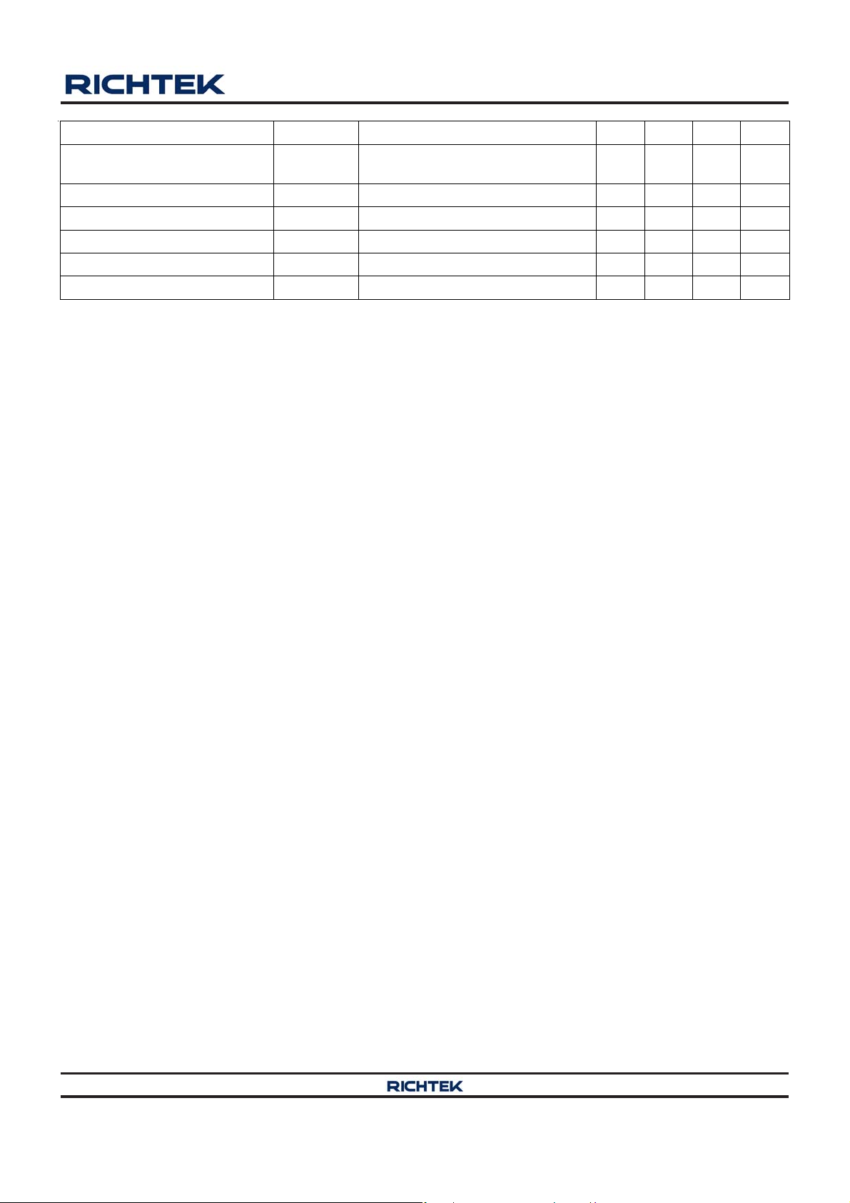
Electrical Characteristics
(V
= 4.5V, T
IN
VI N POR Ri si ng Thresh old
Voltage
VIN POR Falling Threshold
Voltage
VIN V
VIN V
VI N Standby Cur rent V
BATT Sleep Leakage Current I
Battery Regulation Voltage V
VIN Power M OSFET
On-Resistance
IS ET Set Volta ge
(Fast Charge Phase)
Cha r ge Cur ren t Acc urac y R
BATT Pre- Cha r ge Thr es hol d V
BATT Pre- Cha r ge Thr es hol d
Hysteresis
Pre-Charge Current I
ENB Input
T hres hol d Vol tag e
Th erm al R egu lati on T
= 25°C unless otherwise specified)
A
Parameter Symbol Test Conditions Min Typ Max Unit
VOS Rising V
BATT
VOS Fa llin g V
BATT
Logic-High V
V
V
SLEEP
R
V
V
CHG_PRE
3.4 3.8 4.2 V
POR_H
3.1 3.5 3.9 V
POR_L
-- 90 150 mV
OS_H
10 50 -- mV
OS_L
-- 1 5 A
4.158 4.2 4.242 V
REG
I
DS(ON)
-- 1.22 -- V
ISET
CHG_PRE
CHG_PRE
2.45 2.55 2.65 V
40 100 150 mV
12 16.7 21.3 %
IH
Logic-Low VIL -- -- 0.4
-- 115 -- C
REG
= 4.5V -- 400 600 A
BATT
= 0.5A -- 0.6 --
BATT
= 24.3k 450 500 550 mA
ISET
= 4.2V to 24V
V
IN
1.5 -- -V
Copyright 2014 Richtek Technology Corporation. All rights reserved. is a registered trademark of Richtek Technology Corporation.
4
©
DS9526A-03 July 2014www.richtek.com
RT9526A
Parameter Symbol Test Conditions Min Typ Max Unit
VIN Over-Voltage Protection
Threshold
VIN OVP Hysteresis V
PGB Pull-Down Voltage 5mA -- 200 -- mV
CHG_SB Pull-Down Voltage 5mA -- 200 -- mV
EOC Current Setting I
EOC Rising Threshold R
Note 1. Stresses beyond those listed “Absolute Maximum Ratings” may cause permanent damage to the device. These are
stress ratings only, and functional operation of the device at these or any other conditions beyond those indicated in
the operational sections of the specifications is not implied. Exposure to absolute maximum rating conditions may
affect device reliability.
Note 2. θ
Note 3. The device is not guaranteed to function outside its operating conditions.
is measured at T
JA
measured at the exposed pad of the package.
A
V
6.7 7 7.5 V
OVP
-- 0.1 -- V
OVP
R
IMIN
= 25°C on a high effective thermal conductivity four-layer test board per JEDEC 51-7. θJC is
= 243k -- 45 -- mA
IMIN
= 24.3k 337.5 375 412.5 mA
IREF
Copyright 2014 Richtek Technology Corporation. All rights reserved. is a registered trademark of Richtek Technology Corporation.
DS9526A-03 July 2014 www.richtek.com
©
5

RT9526A
Typical Application Circuit
Adapter or USB
R
R
C
IN
ISET
IMIN
VIN
ISET
IMIN
GND
ENB
RT9526A
CHG_SB
BATT
PGB
R1
R2
C
OUT
V
BATT
V
BATT
Copyright 2014 Richtek Technology Corporation. All rights reserved. is a registered trademark of Richtek Technology Corporation.
©
DS9526A-03 July 2014www.richtek.com
6

Typical Operating Characteristics
)
)
RT9526A
VOUT Regulation Voltage vs . Input Voltage
4.2420
4.2252
4.2084
4.1916
4.1748
VOUT Regul ation Voltage (V) 1
4.1580
4.5 5 5.5 6 6.5 7
Inp ut Voltage (V)
Charge Current vs. Input Voltage
550
540
530
520
510
500
490
480
470
Charge Current (m A
460
450
4 4.5 5 5.5 6 6.5 7
V
= 3.8V, R
BATT
Input Voltage (V)
= 24.3kΩ
ISET
BATT Sleep Leakage Current vs. Battery Voltage
5.0
4.5
4.0
3.5
3.0
2.5
2.0
1.5
1.0
0.5
BATT Sleep Leakage Current (µ A) 1
0.0
1 1.5 2 2.5 3 3.5 4 4.5
Bat tery Volt age (V)
Pre-Charge Current vs. Input Voltage
95
91
87
83
79
Pre- C harge Current (mA
V
= 3.8V, R
75
44.555.566.57
BATT
Input Voltage (V)
= 24.3kΩ
ISET
1.25
1.24
1.23
ISET Voltage vs. Input Voltage
V
IN
(10V/Div)
V
BATT
OVP
ENB : Low
(2V/Div)
1.22
V
ISET Voltage (V)
1.21
V
= 3.8V, R
1.20
4 4.5 5 5.5 6 6.5 7
BATT
= 24.3kΩ
ISET
CHG_SB
(2V/Div)
I
CHG
(500mA/Div)
VIN = 0V to 12V, V
Time (500μs/Div)
BATT
= 3.8V, R
= 24.3kΩ
ISET
Input Voltage (V)
Copyright 2014 Richtek Technology Corporation. All rights reserved. is a registered trademark of Richtek Technology Corporation.
©
DS9526A-03 July 2014 www.richtek.com
7

RT9526A
V
IN
(5V/Div)
V
BATT
(2V/Div)
V
CHG_SB
(2V/Div)
I
CHG
(500mA/Div)
Power On
V
= 3.8V , R
BATT
Time (500μs/Div)
ENB : Low
= 24.3kΩ
ISET
V
IN
(5V/Div)
V
BATT
(2V/Div)
V
CHG_SB
(2V/Div)
I
CHG
(500mA/Div)
Shutdown
V
= 3.8V, R
BATT
Time (5ms/Div)
ENB : Low
= 24.3kΩ
ISET
Copyright 2014 Richtek Technology Corporation. All rights reserved. is a registered trademark of Richtek Technology Corporation.
©
DS9526A-03 July 2014www.richtek.com
8

Application Information
RT9526A
The RT9526A is a fully integrated low cost single cell Liion battery charger operable in Constant Current (CC) mode
or Constant Voltage (CV) mode. The CC mode current is
set with the external resistor, R
, and the CV mode
ISET
voltage is fixed at 4.2V. If the battery voltage is below a
typical 2.55V pre-charge threshold, the RT9526A charges
the battery with a trickle current until the battery voltage
rises above the pre-charge threshold. The RT9526A is
cap able of being powered up from AC adapter and USB
(Universal Seri al Bus) port inputs.
VIN Over-Voltage Protection
The input voltage is monitored by the internal comparator .
The OVP threshold is set at 7V (typ.). When the input
voltage exceeds the threshold, the controller outputs a
logic signal to turn off the power P-MOSFET to prevent
the electronics in the handheld system from damaging
due to high input voltage. Neverthele ss, an AC in put voltage
over 28V will still da mage the RT9526A. When the input
over-voltage condition is removed, the controller will enable
the output again by running through soft-start.
Charger Enable Input
ENB is an active-low logic input to enable the charger.
Drive the ENB pin low or leave it floating to enable the
charger. This pin has a 200kΩ internal pull-down resistor .
So when left floating, the input is equivalent to logic-low.
Drive this pin high to disable the charger.
Battery Charge Profile
The RT9526A charges a Li-ion battery under Constant
Current (CC) mode or Constant Voltage (CV) mode. The
constant current of ISET is set via the external resistor,
R
, and the consta nt voltage is fixed at 4.2V . If the battery
ISET
voltage is below a typical 2.55V pre-charge threshold, the
RT9526A charges the battery with a trickle current until
the battery voltage rises above the pre-charge threshold.
When the battery voltage reaches 4.2V , the charger enters
CV mode and regulates the battery voltage at 4.2V to
fully charge the battery without the risk of over charge.
CVCCTrickle
4.2V
I
CHG_FAST
2.8V
16.7 %
I
CHG_FAST
CHG_SB
Charge
Current
I
IMIN
CHG
Indication
Charge
Voltage
Figure 1. T ypical Charge Profile
a. Battery Pre-Charge Current
During a charge cycle, if the battery voltage is below the
pre-charge threshold, the RT9526A applies a pre-charge
mode to the battery . This feature revives deeply discharged
cells and protects battery life. The internally determined
pre-charge rate of the RT9526A is 16.7% of the con stant
charge current.
b. Battery Fast-Charge Current (CC Mode)
The RT9526A of fers ISET pin to determine the fast-charge
current via an external re sistor, R
, connected between
ISET
ISET and GND. The fa st-charge current can be calculated
by the following equation :
V
I = K x (mA)
CHG_FAST ISET
K
= 9959; V
SET
SET
Battery Cha rge Current vs. R
1400
1200
1000
800
600
400
200
Battery Charge Current (mA) 1
0
10 19 28 37 46 55
ISET
R
ISET
= 1.22 (typ.)
R
ISET
Ω
(k )
ISET
Figure 2
75 %
I
CHG_FAST
Time
Copyright 2014 Richtek Technology Corporation. All rights reserved. is a registered trademark of Richtek Technology Corporation.
©
DS9526A-03 July 2014 www.richtek.com
9
RT9526A
c. Battery Voltage Regulation (CV Mode)
The battery voltage regulation feedback is through the
BATT pin. The RT9526A monitors the battery voltage
between the BA TT and GND pins. When battery voltage is
close to battery regulation voltage threshold, the voltage
regulation phase begin s and the charging current begins
to taper down. When battery voltage is over battery
regulation voltage threshold and charge mode stops, the
RT9526A still monitors the battery voltage. Charge current
is resumed when the battery voltage falls under battery
regulation voltage threshold.
Sleep Mode
The RT9526A enters sleep mode if both AC a nd USB are
removed from the input. This feature prevents draining the
battery during the absence of input supply.
Power Good
This open-drain output pin is used to indicate the input
voltage status. The PGB output a sserts low when
1. VIN > V
2. VIN
−−
− V
−−
POR
BATT
> V
OS
Upon reaching the End-Of-Charge (EOC) current, the
charger indicates charge completion via the CHG_SB pin,
but the charger continues to output 4.2V voltage. Figure
1 shows the typical charge profile and the EOC/reset
event. The CHG_SB signal asserts low when the trickle
charge starts and cha nges to high at EOC. After EOC is
reached, the charge current has to rise above 75% of
I
CHG_FAST
before the CHG_SB signal is allowed to turn on
again. A current surge after EOC may occur due to a load
connected to the battery.
Temperature Regulation and Thermal Protection
In order to maximize charge rate, the RT9526A features a
junction temperature regulation loop. If the power
dissipation of the IC results in junction temperature greater
than the thermal regulation threshold (1 15°C), the RT9526A
will cut back on the charge current and disconnect the
battery in order to maintain thermal regulation at around
115°C. This operation continues until the junction
temperature falls below thermal regulation threshold
(115°C) by the hysteresis level. This feature prevents the
maximum power dissipation from exceeding typical design
conditions.
3. VIN < V
OVP
It can be used to drive an LED or communicate to the
host processor. Note that ON indicates the open-drain
transistor is turned on a nd LED is bright.
CHG_SB Indication
The CHG_SB pin is an open-drain output capable to at
lea st 10mA current when the charger starts to charge a nd
turns off when the EOC current is rea ched. The CHG_SB
signal is interfaced either with a micro processor GPIO or
an LED for indication.
End-Of-Charge Current (EOC)
Connect a resistor between the IMIN pin a nd GND to set
the EOC current. The EOC current level, I
programmable via the external resistor, R
IMIN
, is
IMIN
(kΩ), as
shown in the following equation :
I =
IMIN
10935
R
IMIN
(mA)
Selecting the Input and Output Capacitors
In most applications, a 1μF high frequency decoupling
cap acitor pla ced in close proximity to the input is sufficient.
However, depending on the power supply chara cteristics
and cable length, it may be nec essary to add an addition al
10μF ceramic capacitor to the input. For the RT9526A, a
small output cap acitor is required f or loop stability . A 1μF
ceramic ca pa citor placed between the BA TT pin and GND
is typically sufficient.
Thermal Considerations
For recommended operating condition specifications, the
maximum junction temperature is 125°C. The junction to
ambient thermal re sistance, θJA, is layout dependent. For
WDFN-8L 2x3 package, the thermal resistance, θJA, is
31.5°C/W on a standard JEDEC 51-7 four-layer thermal
test board. For SOT-23-6 pa ckage, the thermal resistance,
θ
, is 208.2°C/W on a standard JEDEC 51-7 four-layer
JA
thermal test board. The maximum power dissipation at T
= 25°C can be calculated by the following f ormula :
A
Copyright 2014 Richtek Technology Corporation. All rights reserved. is a registered trademark of Richtek Technology Corporation.
10
©
DS9526A-03 July 2014www.richtek.com

RT9526A
P
= (125°C − 25°C) / (31.5°C/W) = 3.17W for
D(MAX)
W DF N-8L 2x3 pa ckage
P
= (125°C − 25°C) / (208.2°C/W) = 0.48W for
D(MAX)
SOT-23-6 pa ckage
The maximum power dissipation depends on the operating
ambient temperature for fixed T
and thermal
J(MAX)
resistance, θJA. The derating curve in Figure 3 allow the
designer to see the effect of rising ambient temperature
on the maximum power dissipation.
4.0
3.5
WDFN-8L 2x3
3.0
2.5
2.0
1.5
1.0
SOT-23-6
0.5
Maximum Power Dissipation (W) 1
0.0
0 25 50 75 100 125
Ambient Tempera ture ( °C )
Four-Layer PCB
Layout Consideration
The RT9526A is a fully integrated low cost single-cell Liion battery charger ideal for portable a pplications. Careful
PCB layout is necessary . For best performance, pla ce all
peripheral components as close to the IC as possible. A
short connection is highly recommended. The following
guidelines should be strictly followed when designing a
PCB layout for the RT9526A.
Input capacitor should be placed close to the IC and
connected to the ground plane. The trace of input on
the PCB should be placed far away from the sensitive
devices and shielded by the ground.
The GND and exposed pad should be connected to a
strong ground plane for heat sinking a nd noise protection.
The connection of R
should be isolated from other
ISET
noisy traces.
Output capacitor should be placed close to the IC and
connected to the ground plane to reduce noise coupling.
Figure 3. Derating Curve of Maxi mum Power Dissi pation
C
should be placed near the
IN
IC to improve performance.
VIN BATT
C
BATT
BATT
R1
CHG_SB
R2
VIN
PGB
ENB
1
2
3
4
Figure 4. PCB Layout Guide
The copper area connecting the
resistors of ISET and IMIN should
be minimized and kept far away
C
OUT
IN
8
BATT
7
ISET
6
GND9IMIN
5
GND
The GND plane should be connected to a strong
ground plane for heat sinking and noise protection.
from noise sources.
R
ISET
R
IMIN
GND
Copyright 2014 Richtek Technology Corporation. All rights reserved. is a registered trademark of Richtek Technology Corporation.
©
DS9526A-03 July 2014 www.richtek.com
11

RT9526A
Outline Dimension
D
E
A
E2
A3
A1
D2
L
SEE DETAIL A
1
e
b
2
1
1
2
DETAIL A
Pin #1 ID a nd T ie Bar Mark Option s
Note : The configuration of the Pin #1 identifier is optional,
but must be located within the zone indicated.
Dimensions In Millimeters Dimensions In Inc hes
Symbol
Min Max Min Max
A 0.700 0.800 0.028 0.031
A1 0.000 0.050 0.000 0.002
A3 0.175 0.250
0.007 0.010
b 0.200 0.300 0.008 0.012
D 1.900 2.100 0.075 0.083
D2 1.550 1.650 0.061 0.065
E 2.900 3.100 0.114 0.122
E2 1.650 1.750 0.065 0.069
e 0.500 0.020
L 0.350 0.450
W-Type 8L DFN 2x3 Package
0.014 0.018
Copyright 2014 Richtek Technology Corporation. All rights reserved. is a registered trademark of Richtek Technology Corporation.
12
©
DS9526A-03 July 2014www.richtek.com

RT9526A
H
D
L
C
b
A
e
B
A1
Dimensions In Millimeters Dimensions In Inches
Symbol
Min Max Min Max
A 0.889 1.295 0.031 0.051
A1 0.000 0.152 0.000 0.006
B 1.397 1.803 0.055 0.071
b 0.250 0.560 0.010 0.022
C 2.591 2.997 0.102 0.118
D 2.692 3.099 0.106 0.122
e 0.838 1.041 0.033 0.041
H 0.080 0.254 0.003 0.010
L 0.300 0.610 0.012 0.024
SOT-23-6 Surface Mount Package
Richtek Technology Corporation
14F, No. 8, Tai Yuen 1st Street, Chupei City
Hsinchu, Taiwan, R.O.C.
Tel: (8863)5526789
Richtek products are sold by description only. Richtek reserves the right to change the circuitry and/or specifications without notice at any time. Customers should
obtain the latest relevant information and data sheets before placing orders and should verify that such information is current and complete. Richtek cannot
assume responsibility for use of any circuitry other than circuitry entirely embodied in a Richtek product. Information furnished by Richtek is believed to be
accurate and reliable. However, no responsibility is assumed by Richtek or its subsidiaries for its use; nor for any infringements of patents or other rights of third
parties which may result from its use. No license is granted by implication or otherwise under any patent or patent rights of Richtek or its subsidiaries.
DS9526A-03 July 2014 www.richtek.com
13

 Loading...