

Page 1
Linear Single Cell Li-Ion Battery Charger IC
RT9513
General Description
The RT9513 is a fully integrated low cost single-cell LiIon battery charger IC ideal for portable a pplications. The
RT9513 is ca pable of being powered up from AC ada pter.
The RT9513 enters sleep mode when AC adapter is
removed.
The RT9513 optimizes the charging ta sk by using a control
algorithm including preconditioning mode, fast charge
mode and constant voltage mode. The charging task is
terminated a s the charge current drops below the preset
threshold. The AC adapter charge current can be
programmed up to 1A with an external resister . The internal
thermal feedback circuitry regulates the die temperature
to optimize the charge rate for all a mbient temperatures.
The RT9513 features 18V maximum rating voltages for
AC adapter. The other features are under voltage
protection, over voltage protection for AC ada pter supply .
Ordering Information
RT9513
Package Type
QW : WDFN-10L 3x3 (W-Type)
Lead Plating System
G : Green (Halogen Free and Pb Free)
Note :
Richtek products are :
` RoHS compliant and compatible with the current require-
ments of IPC/JEDEC J-STD-020.
` Suitable for use in SnPb or Pb-free soldering processes.
Features
zz
z
18V Maximum Rating for AC Adapter
zz
zz
z Internal Integrate P-MOSFETs
zz
zz
z AC Adapter Power Good Status Indicator
zz
zz
z Charge Status Indicator
zz
zz
z Under Voltage Protection
zz
zz
z Over Voltage Protection
zz
zz
z Automatic Recharge Feature
zz
zz
z Small 10-Lead WDFN Package
zz
zz
z Thermal Feedback Optimizing Charge Rate
zz
zz
z RoHS Compliant and Halogen Free
zz
Applications
z Digital Camera s
z Cellular Phones
z Personal Data Assistants (PDAs)
z MP3 Players
z Hand Held PCs
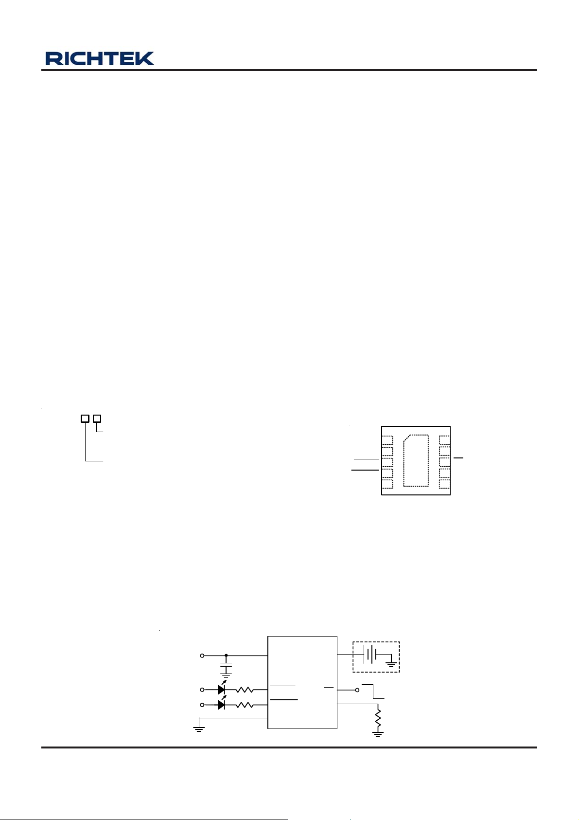
Pin Configurations
(TOP VIEW)
ACIN
NC
CHG_S
PGOOD
GND
1
2
3
GND
4
5
WDFN-10L 3x3
10
BATT
9
NC
8
EN
7
NC
9
11
ISETA
Marking Information
For marking information, contact our sales representative
directly or through a Richtek distributor located in your
area.
Typical Application Circuit
Battery Pack
AC
Adapter
To System
To System
1uF
Exposed Pad (11)
1
ACIN
3
CHG_S
4
PGOOD
5,
GND
RT9513
DS9513-01 April 2011 www.richtek.com
BATT
EN
ISETA
10
+
Chip Shutdown
8
6
Chip Enable
R
SET
1
Page 2
RT9513
Functional Pin Description
Pin No. Pin Name Pin Function
1 ACIN
2, 7, 9 NC
3
CHG_S
4 PGOOD
5 GND
6 ISETA
8
EN
10 BATT
Exposed Pad (11) GND
Wall Adaptor Charge Input Supply.
No Internal Connection.
Charge Status Indicator Output (open drain).
Power Good Indicator Output (open drain).
Ground.
Wall Adaptor Supply Charge Current Set Point.
Charge Enable Input (active low).
Battery Charge Current Output.
Gr oun d. The ex pos ed pad must be sold er ed to a lar ge PCB and conne ct ed to
GND for maximum power dissipation.
Function Block Diagram
GND
Charge Input
Selection
SENSE
FET
ACIN
ACIN
PFET
Comparator
2.5V
OVP
+
-
OVP
ISETA
0.25V
Current
Amplifier
Tcrmination
Comparator
0.25V
0.9V
2.5V
0.5V
BATT
V
REF
Thermal
Sense
115 C
2.5V
-
Precharge
+
Charge
-
Disable
+
1uA
+
V/I
0.25V
2.5V
+
-
V/I
+
-
Voltage
Amplifier
Charge Done
Precharge
Comparator
2.5V
Comparator
2.5V
VCC
Logic
+
-
Recharge
+
-
Precharge
Recharge
PGOOD
CHG_S
EN
DS9513-01 April 2011www.richtek.com
2
Page 3
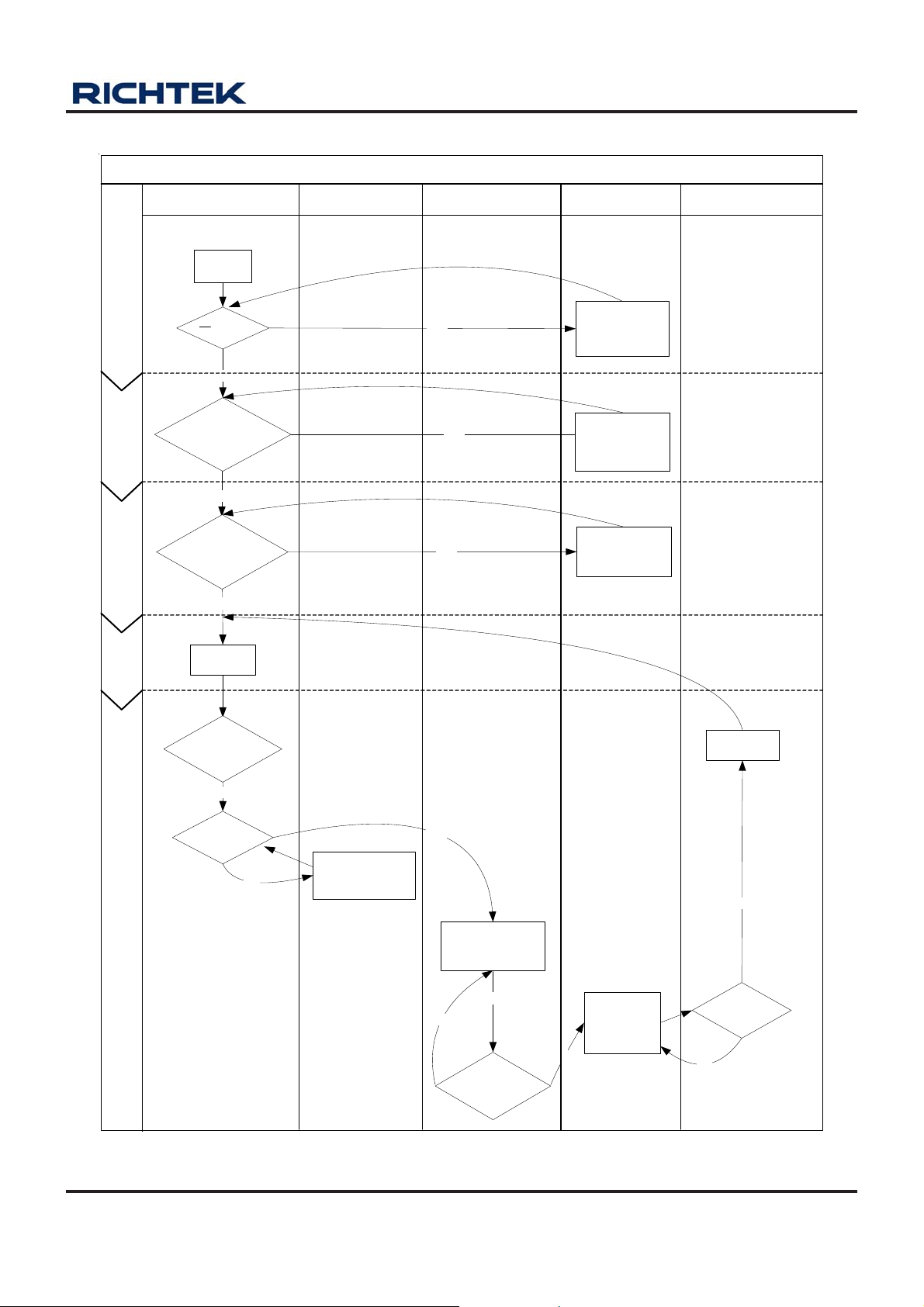
RT9513 Flow Chart
RT9513
Table
Start-Up Precharge Phase Fast Charge Phase Standby/Fault Recharge Phase
ACIN
Power Up
DISABLE MODE
V
EN
> 1.4V ?
YES
P-MOSFET OFF
= 0
I
BATT
DISABLEUVP / OVPSLEEPStart-Up
V
ACIN
V
ACIN
V
ACIN
1ms Delay
V
TS
V
TS
NO
> 6.5V or
< 4.4V?
NO
< V
BATT
NO
> 2.5V
or
< 0.5V?
NO
YES
?
YES
OVP/UVP MODE
P-MOSFET OFF
= 0
I
BATT
SLEEP MODE
P-MOSFET OFF
= 0
I
BATT
RECHARGE
V
BATT
> 2.8V?
NO
I
= 0.1 Charge
BATT
Current
/CHG_S Pull Down
YES
YES
I
= Charge
BATT
Current
/CHG_S Pull Down
NO
V
I
BATT
YES
BATT ~
< 0.1 I
4.2V,
CHG
?
YES
STANDBY
PFET OFF
V
BATT
I
BATT
= 4.2V,
= 0
NO
V
BATT
> 4.1 V?
DS9513-01 April 2011 www.richtek.com
3
Page 4

RT9513
Absolute Maximum Ratings (Note 1)
z AC Input Voltage----------------------------------------------------------------------------------------------------------- −0.3V to 18V
z EN Input Voltage----------------------------------------------------------------------------------------------------------- −0.3V to 6V
z Output Current ------------------------------------------------------------------------------------------------------------- 1.2A
z Power Dissipation, P
W D FN-10L 3x3------------------------------------------------------------------------------------------------------------- 0.926W
z Package Thermal Re sistance (Note 2)
W DFN-10L 3x3, θJA------------------------------------------------------------------------------------------------------- 108 °C/W
WDFN-10L 3x3, θJC------------------------------------------------------------------------------------------------------- 8.2°C/W
z Lead Te mperature (Soldering, 10 sec.)------------------------------------------------------------------------------- 26 0°C
z Junction T emperature ---------------------------------------------------------------------------------------------------- 150°C
z Storage T emperature Range -------------------------------------------------------------------------------------------- −65°C to 150°C
z ESD Susceptibility (Note 3)
HBM (Human Body Mode) ---------------------------------------------------------------------------------------------- 2kV
MM (Ma chine Mode)------------------------------------------------------------------------------------------------------ 200V
Recommended Operating Conditions (Note 4)
z Junction T emperature Range-------------------------------------------------------------------------------------------- −40°C to 125°C
z Ambient T emperature Range-------------------------------------------------------------------------------------------- −40°C to 85°C
@ TA = 25°C
D
Electrical Characteristics
(ACIN = 5V, TA = 27°C, Unless Otherwise specification)
Parameter Symbol Test Conditions Min Typ Max Units
Supply Input
ACIN Input Voltage Range V
ACIN UVP Rising Threshold Voltage V
ACIN UVP Hysteresis V
ACIN Standby Current I
ACIN Shutdown Current I
ACIN UVP Current I
BATT Sleep Leakage Current I
4.5 --
ACIN
UV_HIGH
UV_LOW
STBY
SHDN
UVP
SLEEP
-- 4.4 4.5 V
50 80 120 mV
V
V
V
= 4.5V -- 300 500 μA
BATT
V
= HIGH
EN
= 4V, V
ACIN
ACIN
= 4V, V
= 3V -- 150 250 μ A
BATT
= 4.5V -- -- 10 μA
BATT
-- 50 100 μA
Voltage Regulation
BATT Regulation Voltage V
I
REG
= 60mA 4.158 4.2 4.242 V
BATT
Regulation Voltage Accuracy −1 -- +1 %
ACIN MOSFET R
DS(ON)_ACIN IBATT
= 500mA -- 600 -- mΩ
Current Regul ation
ISETA Set Voltage
(Fast Charge Phase)
Full Charge Setting Range I
AC Charge Current accuracy I
V
V
ISETA
CHG_AC
CHG_AC
100 -- 1200 mA
V
= 3.5V 2.45 2.5 2.55 V
BATT
BATT
= 3.8V, R
= 1.5kΩ -- 500 -- mA
ISET
6 V
To be continued
DS9513-01 April 2011www.richtek.com
4
Page 5

Precharge
y
RT9513
Parameter Symbol Test Conditions Min Typ Max Units
BATT Pre-Charge Rising Threshold V
BATT Pre-Charge Threshold
steresis
H
Pre-Charge Current I
ΔV
PCHG
2.6 2.8 3 V
PRECH
50 100 200 mV
PRECH
V
= 2V 8 10 12 %
BATT
Recharge Threshold
BATT Re-Charge Falling Threshold
Hysteresis
ΔV
RECH_L
V
REG
− V
60 100 150 mV
BATT
Charge Termination Detection
Termination Curren t Ratio (default) I
V
TERM
= 4.2V -- 10 -- %
BATT
Logic Input/Output
CHG_S Pull Down Voltage V
PGOOD Pull Down Voltage V
EN Threshold
Logic-High Voltage V
TBD, I
CHG_S
PGOOD
IH
TBD, I
1.5 -- -- V
CHG_S
PGOOD
= 5mA
= 5mA -- 220 -- mV
-- 65 -- mV
Logic-Low Voltage VIL -- -- 0.4 V
EN Pin Input Current IEN V
= 2V -- -- 2 μA
EN
Protection
Thermal Regulation -- 125 -- °C
OVP SET Internal Default -- 6.5 -- V
Note 1. Stresses listed as the above “Absolute Maximum Ratings” may cause permanent damage to the device. These are for
stress ratings. Functional operation of the device at these or any other conditions beyond those indicated in the
operational sections of the specifications is not implied. Exposure to absolute maximum rating conditions for extended
periods may remain possibility to affect device reliability.
Note 2. θJA is measured in the natural convection at TA = 25°C on a high effective thermal conductivity test board (4 layers, 1S)
of JEDEC 51-7 thermal measurement standard. The case point of θ
Note 3. Devices are ESD sensitive. Handling precaution is recommended.
Note 4. The device is not guaranteed to function outside its operating conditions.
is on the expose pad for the package.
JC
DS9513-01 April 2011 www.richtek.com
5
Page 6

RT9513
Typical Operating Characteristics
V
ACIN
(5V/Div)
V
BATT
(2V/Div)
CHG_S
(5V/Div)
I
CHARGE
(0.5A/Div)
V
ACIN
(5V/Div)
V
BATT
(2V/Div)
CHG_S
(5V/Div)
I
CHARGE
(0.5A/Div)
ACIN Power On
V
ACIN
ACIN Power Off
(5V/Div)
V
BATT
(2V/Div)
CHG_S
(5V/Div)
I
CHARGE
(0.5A/Div)
V
= 3.7V
BATT
Time (250μs/Div)
ACIN OVP
V
V
OUT
V
BATT
V
IN
(2V/Div)
V
ACIN
OUT
V
IN
Time (500μs/Div)
ACIN OVP
V
BATT
= 3.7V
(5V/Div)
CHG_S
(5V/Div)
I
CHARGE
ACIN = 0V to 10V, V
BATT
= 3.7V
(0.5A/Div)
ACIN = 5V to 8V to 5V, V
BATT
= 3.7V
V
(5V/Div)
CHG_S
(5V/Div)
I
CHARGE
(1A/Div)
6
ACIN
Time (1ms/Div)
Input Voltage Transition
ACIN Power Off
V
BATT
Time (500μs/Div)
= 3.7V
V
ACIN
(5V/Div)
CHG_S
(5V/Div)
I
CHARGE
(1A/Div)
Time (1ms/Div)
Input Voltage Transition
ACIN Power On
V
BATT
Time (500μs/Div)
DS9513-01 April 2011www.richtek.com
= 3.7V
Page 7

Application Information
RT9513
Automatically Power Source Selection
The RT9513 is a battery charger IC which is designed for
Li-ion Battery with 4.2V rated voltage.
AC Mode : When the AC input voltage (ACIN) is higher
than the UVP voltage level (4.4V), the R T9513 will enter
AC Mode. In the AC Mode, ACIN P-MOSFET is turned on
and USB P-MOSFET is turned of f.
Sleep Mode : The RT9513 will enter Sleep Mode when
AC input voltage are removed. This feature provides low
leakage current from the battery during the absence of
input supply.
ACIN Over Voltage Protection
The AC input voltage is monitored by an internal OVP
comparator. The comparator ha s a n accurate reference of
2.5V from the band-ga p reference. The OVP threshold is
set by the internal resistive. The protection threshold is
set to 6.5V . When the input voltage exceeds the threshold,
the comparator outputs a logic signal to turn off the power
P-MOSFET to prevent the high input voltage from da maging
the electronics in the handheld system. When the input
over oltage condition is removed (ACIN < 6V), the
comparator re-enables the output by running through the
soft-start.
1200
1000
800
600
400
Charge Current (mA)
200
Fast-Charge Current Setting
The RT9513 offers ISET A pin to determine the AC charge
rate from 100mA to 1.2A. The charge current can be
calculated as f ollowing equation.
V
I = K
charge_ac SET
The parameter K
SET
R
SETA
= 300 ; V
SET
= 2.5V. R
SET
SETA
is the
resistor connected between the ISET A a nd GND.
Pre- Charge Current Setting
During a charge cycle if the battery voltage is below the
VPRECH threshold, the RT9513 a pplies a pre-charge mode
to the battery . This feature revives deeply discharged cells
and protects battery life. The RT9513 internal determines
the pre-charge rate as 10% of the fa st-charge current.
Battery Voltage Regulation
The RT9513 monitors the battery voltage through the BA TT
pin. Once the battery voltage level closes to the VREG
threshold, the RT9513 voltage enters constant pha se a nd
the charging current begins to ta per down. When battery
voltage is over the VREG threshold, the RT9513 will stop
charge and keep to monitor the battery voltage. However ,
when the battery voltage decreases 100mV below the
V
, it will be recharged to keep the battery voltage.
REG
Charge Status Outputs
The open-drain CHG_S and PGOOD outputs indicate
various charger operations a s shown in the following table.
These status pins can be used to drive LEDs or
communicate to the host processor. Note that ON
indicates the open-drain transistor is turned on a nd LED
is bright.
Charge State CHG_S PGOOD
0
0.5 1.5 2.5 3.5 4.5 5.5 6.5 7.5 8.5 9.5
R
(kΩ)
SETA
ACIN
Charge ON ON
Ch arge done OF F ON
Figure 1. AC Mode Charge Current Setting
DS9513-01 April 2011 www.richtek.com
7
Page 8

RT9513
Temperature Regulation and Thermal Protection
In order to maximize the charge rate, the RT9513 features a junction temperature regulation loop. If the power dissipation
of the IC results in a junction temperature greater than the thermal regulation threshold (125°C), the RT9513 throttles
back on the charge current in order to maintain a junction temperature around the thermal regulation threshold (125°C).
The RT9513 monitors the junction temperature, TJ, of the die and disconnects the battery from the input if TJ exceeds
125°C. This operation continues until junction temperature falls below thermal regulation threshold (125°C) by the
hysteresis level. This feature prevents the chip from da mage.
Selecting the Input and Output Capacitors
In most application s, the most importa nt is the high-frequency decoupling capacitor on the input of the RT9513. A 1uF
ceramic ca pa citor , placed in close proximity to in put pin and GND pin is re commended. In some application s depending
on the power supply characteristics a nd cable length, it may be necessary to add a n addition al 10uF cera mic ca pa citor
to the input. The RT9513 requires a small output ca pa citor for loop stability . A 1uF cera mic ca pa citor placed between the
BA TT pin and GND is typically sufficient.
Layout Consideration
The RT9513 is a fully integrated low cost single-cell Li- Ion battery charger ideal for portable a pplications. Careful PCB
layout is necessary. For best performance, place all peripheral components as close to the IC as possible. A short
connection is highly recommended. The following guidelines should be strictly followed when designing a PCB layout
for the RT9513.
` Input ca pa citor should be pla ced close to IC a nd connected to ground plane. The trace of in put in the PCB should be
placed far away the sensitive devices or shielded by the ground.
` The GND should be connected to a strong ground pla ne f or heat sinking and noise protection.
` The connection of R
should be isolated from other noisy traces. The short wire is recommended to prevent EMI and
SETA
noise coupling.
` Output ca pa citor should be pla ced close to IC a nd connected to ground pla ne to reduce noise coupling.
The capacitor should be
placed close to IC pin and
connected to ground plane.
C1
ACIN
NC
CHG_S
PGOOD
GND
1
2
3
4
5
GND
10
9
8
7
9
BATT
NC
EN
NC
ISETA
R
C3
SETA
GND
The GND should be
connected to a strong
ground plane for heat
sinking and noise
protection.
The connection of R
should be isolated from other
noisy traces. The short wire
is recommended to prevent
EMI and noise coupling.
SETA
Figure 2
DS9513-01 April 2011www.richtek.com
8
Page 9

Outline Dimension
RT9513
D
E
A
A3
A1
D2
L
E2
SEE DETAIL A
1
e
b
2
1
DETAIL A
1
2
Pin #1 ID a nd T ie Bar Mark Option s
Note : The configuration of the Pin #1 identifier is optional,
but must be located within the zone indicated.
Dimensions In Millimeters Dimensions In Inches
Symbol
Min Max Min Max
A 0.700 0.800 0.028 0.031
A1 0.000 0.050 0.000 0.002
A3 0.175 0.250 0.007 0.010
b 0.180 0.300 0.007 0.012
D 2.950 3.050 0.116 0.120
D2 2.300 2.650 0.091 0.104
E 2.950 3.050 0.116 0.120
E2 1.500 1.750 0.059 0.069
e 0.500 0.020
L 0.350 0.450
Richtek Technology Corporation
Headquarter
5F, No. 20, Taiyuen Street, Chupei City
Hsinchu, Taiwan, R.O.C.
Tel: (8863)5526789 Fax: (8863)5526611
0.014 0.018
W-Type 10L DFN 3x3 Package
Richtek Technology Corporation
Taipei Office (Marketing)
5F, No. 95, Minchiuan Road, Hsintien City
Taipei County, Taiwan, R.O.C.
Tel: (8862)86672399 Fax: (8862)86672377
Email: marketing@richtek.com
Information that is provided by Richtek Technology Corporation is believed to be accurate and reliable. Richtek reserves the right to make any change in circuit
design, specification or other related things if necessary without notice at any time. No third party intellectual property infringement of the applications should be
guaranteed by users when integrating Richtek products into any application. No legal responsibility for any said applications is assumed by Richtek.
DS9513-01 April 2011 www.richtek.com
9
Page 10

 Loading...