

Page 1
®
3A High Performance Step-Up DC/DC Converter
RT9297
General Description
The RT9297 includes a high performance step-up DC/DC
converter that provides a regulated supply voltage for active-
matrix thin-film transistor (TFT) liquid-crystal displays
(LCDs).
The Boost Converter incorporates current mode, fixed-
frequency, pulse-width modulation (PWM) circuitry with
a built-in N-Channel power MOSFET to achieve high
efficiency and fast transient response.
The RT9297 is available in a WDFN -10L 3x3 package.
Ordering Information
RT9297
Package Type
QW : WDFN-10L 3x3 (W-Type)
Lead Plating System
G : Green (Halogen Free and Pb Free)
Note :
Richtek products are :
` RoHS compliant and compatible with the current require-
ments of IPC/JEDEC J-STD-020.
` Suitable for use in SnPb or Pb-free soldering processes.
Features
zz
High Efficiency Up to 90%
z
zz
zz
z Adjustable Output Voltage : V
zz
zz
z Wide Input Supply Voltage : 2.6V to 5.5V
zz
zz
z Input Under Voltage Lockout
zz
zz
z Pin-Programmable Switching Frequency 640kHz/
zz
to 24V
DD
1.2MHz
zz
z Programmable Soft-Start
zz
zz
z Small 10-Lead WDFN Package
zz
zz
z RoHS Compliant and Halogen Free
zz
Applications
z Notebook Computer Displays
z LCD Monitor Panels
z LCD TV Panels
Pin Configurations
(TOP VIEW)
COMP
FB
EN
GND
GND
1
2
3
4
5
10
SS
9
FREQ
8
VDD
GND
7
LX
11
6
LX
WDFN-10L 3x3
Marking Information
EZ= : Product Code
EZ=YM
YMDNN : Date Code
DNN
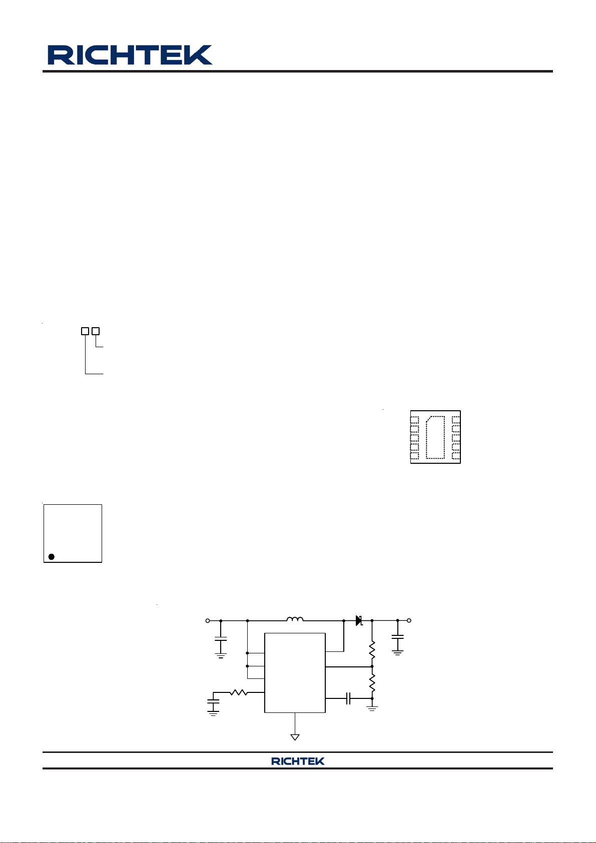
Typical Application Circuit
RT9297
VDD
FREQ
EN
COMP
L1
LX
FB
SS
GND
4, 5,
11 (Exposed Pad)
V
2.6V to 5.5V
Copyright 2012 Richtek Technology Corporation. All rights reserved. is a registered trademark of Richtek Technology Corporation.
©
DD
C3
C1
R3
8
9
3
1
DS9297-02 June 2012 www.richtek.com
6, 7
2
10
D1
R1
C
SS
R2
C2
V
AVDD
1
Page 2
RT9297
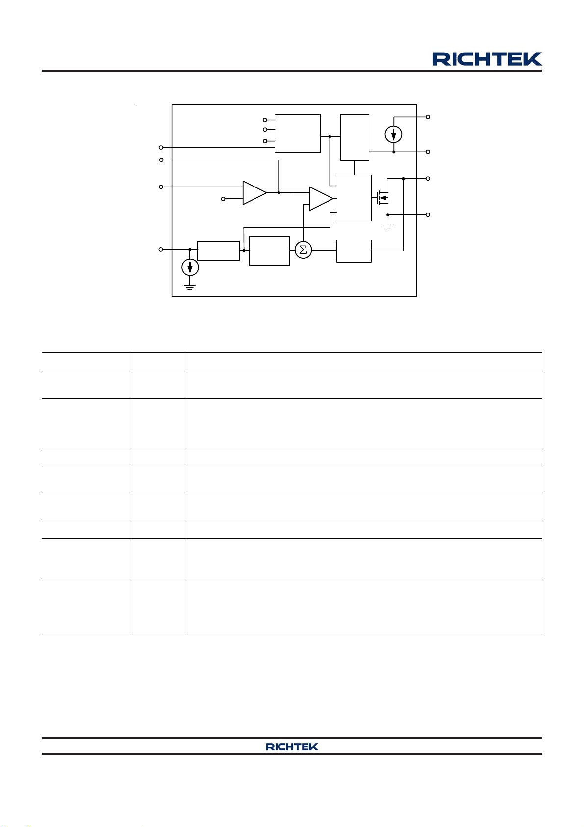
Function Block Diagram
EN
COMP
FB
1.24V
FREQ
Oscillator
4µA
Functional Pin Description
Pin No. Pin Name Pin Function
1 COMP
2 FB
Compensation Pin for Error Amplifier. Connect a series RC fr om CO MP to
ground.
Feedback. The feedback regulation voltage is 1.24V nominal. Connect an
external resistive voltage-divider between the step-up regulator’s output (V
and GND, with the center tap connected to FB. Place the divider close to the IC
and minimize the trace area to reduce noise coupling.
LX
V
IN
V
FB
Error
Amplifier
-
+
Slope
Compen-
sation
Protection
Summing
Comparator
Clock
4µA
SoftStart
-
+
Control
and
Driver
Logic
Current
Sense
VDD
SS
LX
GND
AVDD
)
3 EN Enable Control Input. Drive EN low to turn off the Boost Converter.
4, 5
11 (Exposed Pad)
6, 7 LX
8 VDD Supply Pin. Bypass VDD with a minimum 1μF ceramic capacitor directly to GND.
9 FREQ
10 SS
GND
Ground. The exposed pad must be soldered to a large PCB and connected to
GND for maximum power dissipation.
Switch. LX is the drain of the internal MOSFET. Connect the inductor/rectifier
diode junction to LX and minimize the trace area for lower EMI.
Frequency-Select Input. When FREQ is low, the oscillator frequency will be set
to 640kHz. When FREQ is high, the frequency will be set to 1.2MHz. This input
has a 6μA pull-down current.
Soft-Start Control. Connect a soft-start capacitor (C
) to this pin. A 4μA
SS
constant current charges the soft-start capacitor. When EN connected to GND,
the soft-start capacitor is discharged. When EN connected to V
soft-start capacitor is charged to V
. Leave floating for not using soft-start.
DD
high, the
DD
Copyright 2012 Richtek Technology Corporation. All rights reserved. is a registered trademark of Richtek Technology Corporation.
2
©
DS9297-02 June 2012www.richtek.com
Page 3
RT9297
Absolute Maximum Ratings (Note 1)
z LX to GND --------------------------------------------------------------------------------------------------------------- −0.3V to 26V
z Other Pins to GND ---------------------------------------------------------------------------------------------------- −0.3V to 6V
z Power Dissipation, P
WDFN-10L 3x3 --------------------------------------------------------------------------------------------------------- 1.667W
z Package Thermal Resistance (Note 2)
WDFN-10L 3x3, θJA--------------------------------------------------------------------------------------------------- 60°C/W
WDFN-10L 3x3, θJC--------------------------------------------------------------------------------------------------- 8.2°C/W
z Lead Temperature (Soldering, 10 sec.)--------------------------------------------------------------------------- 260°C
z Junction Temperature ------------------------------------------------------------------------------------------------- 150°C
z Storage Temperature Range ---------------------------------------------------------------------------------------- −65°C to 150°C
z ESD Susceptibility (Note 3)
HBM (Human Body Model)------------------------------------------------------------------------------------------ 2kV
MM (Machine Model) ------------------------------------------------------------------------------------------------- 200V
Recommended Operating Conditions (Note 4)
z Supply Input Voltage, VDD ------------------------------------------------------------------------------------------ 2.6V to 5.5V
z Junction Temperature Range ---------------------------------------------------------------------------------------- −40°C to 125°C
z Ambient Temperature Range ---------------------------------------------------------------------------------------- −40°C to 85°C
@ T
D
= 25°C
A
Electrical Characteristics
(VDD = 3.3V, T
Supply Current
Input Voltage Range VDD
Output Voltage Range V
Under-Voltage Lockout
Threshold
Quiescent Current IQ
Shutdown Current I
Oscillator
Oscillator Frequency f
Maximum Duty Cycle -- 90 -- %
Error Amplifier
Feedback Regulation Voltage VFB 1.22 1.24 1.26 V
Feedback Input Bias Current I
= 25°C, unless otherwise specified)
A
Parameter Symbol Test Conditions Min Typ Max Unit
V
< 18V 2.6 -- 5.5
AVDD
18V < V
VDD -- 24 V
AVDD
V
VDD Rising -- 2.4 -- V
UVLO
< 24V 4 -- 5.5
AVD D
V
Hysteresis -- 50 -- mV
V
= 1.3V, LX Not Switching -- 0.5 --
FB
V
= 1V, LX Switching -- 4 --
FB
EN = GND -- 0.1 10 μA
SHDN
mA
FREQ = GND 500 640 750
OSC
-- 125 250 nA
FB
FREQ = V
1000 1240 1500
lN
kHz
Copyright 2012 Richtek Technology Corporation. All rights reserved. is a registered trademark of Richtek Technology Corporation.
DS9297-02 June 2012 www.richtek.com
©
3
Page 4
RT9297
Parameter Symbol Test Conditions Min Typ Max Unit
Feedback Line Regulation -- 0.05 0.2 %/V
Transconductance gm ΔI = ±2.5μA at COMP = 1V -- 135 -- μA/V
Voltage Gain Av FB to COMP -- 700 -- V/V
N- MOSFET
Current Limit I
On-Resistance R
Leakage Current I
LIM
DS(ON)
LEAK
Current-Sense Transresistance RCS -- 0.25 -- V/A
Soft-Start
Charge Current ISS -- 4 -- μA
Control Inputs
EN, FREQ Input Low Voltage VIL -- -- 0.3 x VDD V
EN, FREQ Input High Voltage VIH 0.7 x VDD -- -- V
EN, FREQ Input Hysteresis -- 0.1 x VDD -- V
FREQ Pull-down Current -- 6 -- μA
EN Input Current IEN EN = GND -- 0.001 1 μA
3 3.8 5 A
-- 125 250 mΩ
VLX = 24V -- 30 45 μA
Note 1. Stresses beyond those listed “Absolute Maximum Ratings” may cause permanent damage to the device. These are
stress ratings only, and functional operation of the device at these or any other conditions beyond those indicated in
the operational sections of the specifications is not implied. Exposure to absolute maximum rating conditions may
affect device reliability.
Note 2. θ
Note 3. Devices are ESD sensitive. Handling precaution is recommended.
Note 4. The device is not guaranteed to function outside its operating conditions.
is measured at T
JA
measured at the exposed pad of the package.
= 25°C on a high effective thermal conductivity four-layer test board per JEDEC 51-7. θJC is
A
Copyright 2012 Richtek Technology Corporation. All rights reserved. is a registered trademark of Richtek Technology Corporation.
4
©
DS9297-02 June 2012www.richtek.com
Page 5

Typical Operating Characteristics
RT9297
Output Voltage (V)
Effic iency vs. Load Current
100
90
80
70
60
50
40
Efficiency (%)
30
20
10
0
0 0.05 0.1 0.15 0.2 0.25 0.3 0.35 0.4
V
= 13.6V, f = 1.2MHz
AVDD
Load Current (A)
Output Voltage vs. Load Current
13.70
13.69
13.68
13.67
13.66
13.65
13.64
13.63
13.62
13.61
13.60
0 0.05 0.1 0.15 0.2 0.25 0.3 0.35 0.4
Load Current (A)
V
= 13.6V, f = 1.2MHz
AVDD
VDD = 5V
VDD = 3.3V
VDD = 5V
VDD = 3.3V
Output Voltage (V)
Efficiency vs. Loa d Current
100
90
80
70
60
50
40
Efficiency (%)
30
20
10
0
0 0.05 0.1 0.15 0.2 0.25 0.3 0.35 0.4
V
= 13.6V, f = 640kHz
AVDD
Load Current (A)
Output Voltage vs. Load Current
13.70
13.69
13.68
13.67
13.66
13.65
13.64
13.63
13.62
13.61
13.60
0 0.05 0.1 0.15 0.2 0.25 0.3 0.35 0.4
Load Current (A)
V
= 13.6V, f = 640kHz
AVDD
VDD = 5V
VDD = 3.3V
VDD = 5V
VDD = 3.3V
Output Voltage v s . Input Voltage
Output Voltage (V)
13.66
13.65
13.64
13.63
13.62
13.61
13.60
13.59
13.58
13.66
13.65
13.64
13.63
Output Voltage (V)
13.62
13.61
13.60
13.59
13.58
2.5 3 3.5 4 4.5 5 5.5
I
= 0mA
AVDD
= 100mA
I
AVDD
I
= 200mA
AVDD
= 300mA
I
AVDD
I
= 400mA
AVDD
f = 1.2MHz
Input Voltage (V)
Copyright 2012 Richtek Technology Corporation. All rights reserved. is a registered trademark of Richtek Technology Corporation.
©
Output Voltage vs. Input Voltage
I
= 0mA
AVDD
= 100mA
I
AVDD
I
= 200mA
AVDD
I
= 300mA
AVDD
= 400mA
I
AVDD
f = 640kHz
2.5 3 3.5 4 4.5 5 5.5
Input Voltage (V)
DS9297-02 June 2012 www.richtek.com
5
Page 6

RT9297
1.40
1.35
1.30
1.25
1.20
1.15
1.10
Switch Frequency (MHz
1.05
1.00
V
DD
(2V/Div)
V
AVDD
(5V/Div)
V
LX
(10V/Div)
Switching Frequency vs. Te m pe rature
VDD = 3.3V
-40 -25 -10 5 20 35 50 65 80 95 110 125
Temperature (°C)
Start Up
1.260
1.256
1.252
1.248
1.244
1.240
1.236
1.232
Reference Voltage (V)
1.228
1.224
1.220
V
DD
(2V/Div)
V
AVDD
(5V/Div)
V
LX
(10V/Div)
Reference Voltage vs. Temperature
VDD = 3.3V, f = 1.2MkHz
-40 -25 -10 5 20 35 50 65 80 95 110 125
Temperature (°C)
Start Up
I
VDD
(1A/Div)
V
AVDD
(500mV/Div)
I
AVDD
(200mA/Div)
V
= 3.3V, V
DD
f = 1.2MHz, I
AVDD
AVDD
= 300mA
Time (2.5ms/Div)
Load Transient Response
V
= 3.3V, V
DD
Time (100μs/Div)
= 13.6V, f = 1.2MHz
AVDD
= 13.6V
I
VDD
(1A/Div)
V
AVDD
(500mV/Div)
I
AVDD
(500mA/Div)
V
= 5V, V
DD
f = 1.2MHz, I
AVDD
AVDD
Time (2.5ms/Div)
Load Transient Response
V
= 5V, V
DD
Time (100μs/Div)
= 13.6V, f = 1.2MHz
AVDD
= 13.6V
= 300mA
Copyright 2012 Richtek Technology Corporation. All rights reserved. is a registered trademark of Richtek Technology Corporation.
©
DS9297-02 June 2012www.richtek.com
6
Page 7

Application Information
A
RT9297
The RT9297 contains a high performance boost regulator
to generate voltage for the panel source driver ICs. The
following content contains the detailed description and
the information of component selection.
Boost Regulator
The boost regulator is a high efficiency current-mode PWM
architecture with 640K / 1.2MHz operation frequency. It
performs fast transient responses to generate source driver
supplies for TFT LCD display. The high operation frequency
allows smaller components used to minimize the
thickness of the LCD panel. The output voltage setting
can be achieved by setting the resistive voltage-divider
sensing at FB pin. The error amplifier varies the COMP
voltage by sensing the FB pin to regulate the output
voltage. For better stability, the slope compensation signal
summed with the current-sense signal will be compared
with the COMP voltage to determine the current trip point
and duty cycle.
Soft-Start
The RT9297 provides soft-start function to minimize the
inrush current. When power on, an internal constant current
charges an external capacitor. The rising voltage rate on
the COMP pin is limited during the charging period and
the inductor peak current will also be limited at the same
time. When power off, the external capacitor will be
discharged for next soft start time.
The soft-start function is implemented by the external
capacitor with a 4μA constant current charging to the soft-
start capacitor. Therefore, the capacitor should be large
enough for output voltage regulation. Typical value for soft-
start capacitor range is 33nF. The available soft-start
capacitor range is from 10nF to 100nF.
Output Voltage Setting
The regulated output voltage is shown as following
equation :
V = 1.24V x 1+
AVDD
⎛⎞
R
1
⎜⎟
R
⎝⎠
2
The recommended value for R2 should be up to 10kΩ
without some sacrificing. To place the resistor divider as
close as possible to the chip can reduce noise sensitivity.
Loop Compensation
The voltage feedback loop can be compensated with an
external compensation network consisted of R
C
. Choose R
COMP
gain for fast transient response and C
to set high frequency integrator
COMP
COMP
and
COMP
to set the
integrator zero to maintain loop stability. For typical
application VDD = 3.3V , V
= 13.6V , C4 = 4.7μF x 3 ,
AVDD
L = 3.6μH, the recommended value for compensation is
as below : R
COMP
= 56kΩ, C
COMP
= 330pF.
Over Current Protection
The RT9297 boost converter has over-current protection
to limit peak inductor current. It prevents large current
from damaging the inductor and diode. During the ON-
time, once the inductor current exceeds the current limit,
the internal LX switch turns off immediately and shortens
the duty cycle. Therefore, the output voltage drops if the
over-current condition occurs. The current limit there
should is also affected by the input voltage, duty cycle
and inductor value.
Over Temperature Protection
The RT9297 boost converter has thermal protection function
to prevent the chip from overheating. When the junction
temperature exceeds 155°C, it will shut down the device.
Once the device cools down by approximately 30°C, it
will start to operate normally. For continuous operation,
do not operate over the maximum junction temperature
rating 125°C.
Inductor Selection
The inductance depends on the maximum input current.
The inductor current ripple is 20% to 40% of maximum
input current that is a general rule. Assume, choose 40%
as the criterion then
V x I
I =
VDD(MAX)
I
= 0.4 x I
RIPPLE
Where η is the efficiency, I
current, I
RIPPLE
VDD AVDD(MAX)
η x V
DD
VDD(MAX)
is the maximum input
IN(MAX)
is the inductor current ripple. Beside, the
input peak current is maximum input current plus half of
inductor current ripple.
Copyright 2012 Richtek Technology Corporation. All rights reserved. is a registered trademark of Richtek Technology Corporation.
DS9297-02 June 2012 www.richtek.com
©
7
Page 8

RT9297
A
I
= 1.2 x I
PEAK
Note that the saturated current of inductor must be greater
than I
PEAK
as follow equation :
L =
0.4 x V x I x f
Where f
system performance, a shielded inductor is preferred to
avoid EMI issue.
Diode Selection
VDD(MAX)
. The inductance can be eventually determined
η x V x V -V
()
is the switching frequency. To consider the
OSC
2
()( )
DD AVDD DD
2
VDD AVDD(MAX) OSC
Input Current
ΔV
OUT1
Inductor Current
Output Current
(1-D)T
S
ΔI
L
Output Ripple
Voltage (ac)
Time
Time
Schottky diode is a good choice for an asynchronous
Boost converter due to the small forward voltage. However,
power dissipation, reverse voltage rating and pulsating peak
current are the important parameters for Schottky diode
selection. It is recommended to choose a suitable diode
whose reverse voltage rating is greater than the maximum
output voltage.
Capacitor Selection
Output ripple voltage is an important index for estimating
the performance. This portion consists of two parts, one
is the product of input current and ESR of output capacitor,
another part is formed by charging and discharging
process of output capacitor. Refer to Figure 1, evaluate
DV
by ideal energy equalization. According to the
OUT1
definition of Q, the Q value can be calculated as following
equation :
⎡⎤
11 1
Q = I I I I I I
= C V
⎛⎞⎛⎞
× + Δ− + −Δ−
IN LOUT IN LOUT
⎜⎟⎜⎟
⎢⎥
22 2
⎝⎠⎝⎠
⎣⎦
V
×× ×Δ
Vf
OUT SW
IN
1
OUT OUT1
where fSW is the switching frequency, and ΔIL is the
inductor ripple current. Move C
estimate the value of ΔV
×
DI
Δ
V =
OUT1
η
OUT
××
Cf
OUT SW
as the following equation :
OUT1
to the left side to
OUT
Finally, by taking ESR into consideration, the overall output
ripple voltage can be determined as the following
equation :
×
DI
Δ×+
V = I ESR
OUT IN
η Cf
OUT
××
OUT SW
Figure 1. The Output Ripple Voltage without the
Contribution of ESR
Input Capacitor Selection
Low ESR ceramic capacitors are recommended for input
capacitor applications. Low ESR will effectively reduce
the input voltage ripple caused by switching operation. A
10μF is sufficient for most applications. Nevertheless, this
value can be decreased for lower output current
requirement. Another consideration is the voltage rating
of the input capacitor must be greater than the maximum
input voltage.
Thermal Considerations
For continuous operation, do not exceed absolute
maximum operation junction temperature. The maximum
power dissipation depends on the thermal resistance of
IC package, PCB layout, the rate of surroundings airflow
and temperature difference between junction to ambient.
The maximum power dissipation can be calculated by
following formula :
P
Where T
D(MAX)
= (T
J(MAX)
− TA ) / θ
J(MAX)
JA
is the maximum operation junction
temperature 125°C, TA is the ambient temperature and
the θJA is the junction to ambient thermal resistance.
For recommended operating conditions specification,
where T
is the maximum junction temperature of the
J(MAX)
die (125°C) and TA is the maximum ambient temperature.
The junction to ambient thermal resistance θJA is layout
Copyright 2012 Richtek Technology Corporation. All rights reserved. is a registered trademark of Richtek Technology Corporation.
8
©
DS9297-02 June 2012www.richtek.com
Page 9

RT9297
)
dependent. For WDFN-10L 3x3 packages, the thermal
resistance θJA is 60°C/W on the standard JEDEC 51-7
four layers thermal test board. The maximum power
dissipation at TA = 25°C can be calculated by following
formula :
P
= (125°C − 25°C) / (60°C/W) = 1.667W for
D(MAX)
WDFN-10L 3x3 package
The maximum power dissipation depends on operating
ambient temperature for fixed T
and thermal
J(MAX)
resistance θJA . The Figure 2 of derating curves allows the
designer to see the effect of rising ambient temperature
on the maximum power allowed.
1.8
1.6
1.4
1.2
1.0
0.8
0.6
0.4
0.2
Maximum Power Dissipation (W
0.0
0 20 40 60 80 100 120 140
Ambient Temperature (°C)
Four Layers PCB
Figure 2. Derating Curve of Maximum Power Dissipation
Layout Considerations
For high frequency switching power supplies, the PCB
layout is important to get good regulation, high efficiency
and stability. The following descriptions are the guidelines
for better PCB layout.
` For good regulation, place the power components as
close as possible. The traces should be wide and short
enough especially for the high-current output loop.
` The feedback voltage-divider resistors must be near the
feedback pin. The divider center trace must be shorter
and the trace must be kept away from any switching
nodes.
` The compensation circuit should be kept away from
the power loops and be shielded with a ground trace to
prevent any noise coupling.
` Minimize the size of the LX node and keep it wide and
shorter. Keep the LX node away from the FB.
` The exposed pad of the chip should be connected to a
strong ground plane for maximum thermal consideration.
The compensation circuit should be
kept away from the power loops and
be shielded with a ground trace to
prevent any noise coupling.
C3
R3
GND
R2
The feedback voltage-divider
resistors must be near the
feedback pin. The divider center
trace must be shorter and the
trace must be kept away from
any switching nodes.
COMP
FB
EN
GND
GND
R1
1
2
3
4
5
10
9
8
GND
7
11
6
For good regulation place the power
components as close as possible.
The traces should be wide and short
especially for the high-current output
loop.
SS
FREQ
VDD
LX
LX
L1
D1
AVDD
C2
C1
+
GND
V
IN
Figure 3. PCB Layout Guide
Copyright 2012 Richtek Technology Corporation. All rights reserved. is a registered trademark of Richtek Technology Corporation.
DS9297-02 June 2012 www.richtek.com
©
9
Page 10

RT9297
Outline Dimension
D
E
A
A3
A1
D2
L
E2
SEE DETAIL A
1
2
e
b
1
1
2
DETAIL A
Pin #1 ID and Tie Bar Mark Options
Note : The configuration of the Pin #1 identifier is optional,
but must be located within the zone indicated.
Dimensions In Millimeters Dimensions In Inch es
Symbol
Min Max Min Max
A 0.700 0.800 0.028 0.031
A1 0.000 0.050 0.000 0.002
A3 0.175 0.250 0.007 0.010
b 0.180 0.300 0.007 0.012
D 2.950 3.050 0.116 0.120
D2 2.300 2.650 0.091 0.104
E 2.950 3.050 0.116 0.120
E2 1.500 1.750 0.059 0.069
e 0.500 0.020
L 0.350 0.450
0.014 0.018
W-Type 10L DFN 3x3 Package
Richtek Technology Corporation
5F, No. 20, Taiyuen Street, Chupei City
Hsinchu, Taiwan, R.O.C.
Tel: (8863)5526789
Richtek products are sold by description only. Richtek reserves the right to change the circuitry and/or specifications without notice at any time. Customers should
obtain the latest relevant information and data sheets before placing orders and should verify that such information is current and complete. Richtek cannot
assume responsibility for use of any circuitry other than circuitry entirely embodied in a Richtek product. Information furnished by Richtek is believed to be
accurate and reliable. However, no responsibility is assumed by Richtek or its subsidiaries for its use; nor for any infringements of patents or other rights of third
parties which may result from its use. No license is granted by implication or otherwise under any patent or patent rights of Richtek or its subsidiaries.
DS9297-02 June 2012www.richtek.com
10
Page 11

 Loading...