

Datasheet RT9293A-20GJ6, RT9293A-20GQWA, RT9293AGJ6, RT9293AGQW, RT9293AGQWA Datasheet (Richtek) [ru]
...Page 1
RT9293
Small Package, High Performance, Asynchronies Boost
for 10 WLED Driver
General Description
The RT9293 is a high frequency, asynchronous boost
converter. The internal MOSFET can support up to 10
White LEDs for backlighting a nd OLED power application,
and the internal soft start function ca n reduce the inrush
current. The device operates with 1-MHz fixed switching
frequency to allow small external components and to
simplify possible EMI problems. For the protection, the
RT9293A provides 50V OVP a nd the RT9293B provides
50V/20V OVP to allow inexpensive and small-output
cap acitors with lower voltage ratings. The LED current is
initially set with the external sense resistor R
SET
. The
RT9293 is available in the tiny pa ckage type TSOT -23-6
and WDFN-8L 2x2 pa ckages to provide the best solution
for PCB space saving and total BOM cost.
Ordering Information
-
RT9293
Note :
Richtek products are :
` RoHS compliant and compatible with the current require-
ments of IPC/JEDEC J-STD-020.
` Suitable for use in SnPb or Pb-free soldering processes.
( )
Package Type
J6 : TSOT-23-6
QW : WDFN-8L 2x2 (W-Type)
Lead Plating System
G : Green (Halogen Free and Pb Free)
OVP Voltage
Default : 50V (RT9293A/B)
20 : 20V (RT9293B)
Feedback Voltage Reference
A : 104mV
B : 300mV
Features
zz
z VIN Operating Range : 2.5V to 5.5V
zz
zz
z Internal Power N-MOSFET Switch
zz
zz
z Wide Range for PWM Dimming (100Hz to200kHz)
zz
zz
z Minimize the External Component Counts
zz
zz
z Internal Soft Start
zz
zz
z Internal Compensation
zz
zz
z Under Voltage Protection
zz
zz
z Over Voltage Protection
zz
zz
z Over Temperature Protection
zz
zz
z Small TSOT-23-6 and 8-Lead WDFN Packages
zz
zz
z RoHS Compliant and Halogen Free
zz
Applications
z Cellular Phones
z Digital Camera s
z PDAs and Smart Phones a nd MP3 and OLED.
z Portable Instruments
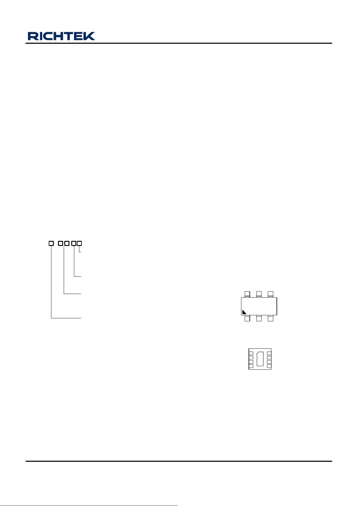
Pin Configurations
(TOP VIEW)
VINVOUT EN
4
56
23
LX GND FB
TSOT-23-6
1
GND
2
VIN
3
VOUT
4
EN
WDFN-8L 2x2
8
LX
7
NC
GND
6
FB
9
5
GND
Marking Information
For marking information, contact our sales re presentative
directly or through a Richtek distributor located in your
area.
DS9293-01 April 2011 www.richtek.com
1
Page 2
RT9293
Typical Application Circuit
22µH to 47µH
L
D
V
OUT
V
IN
Chip Enable
C
2.2µF
Functional Pin Description
Pin No.
RT9293□GJ6 RT9293□GQW
1 8 LX Switching Pin.
2
1, 5,
9 (Exposed pad)
3 6 FB Feedback Pin, put a resistor to GND to setting the current.
4 4 EN Chip Enable (A ctive High).
5 3 VOUT Output Voltage Pin.
6 2 VIN Input Supply.
Pin Name Pin Function
GND
LX
VIN
IN
EN
GND
RT9293
VOUT
FB
C
OUT
1µF
10 WLEDs
R
SET
Ground Pin. The exposed pad must be soldered to a large
PCB and connected to GND for maximum power dis sipation.
-- 7 NC No Internal Connection.
Function Block Diagram
Internal
Compensation
Internal
Soft Start
EA
GM
-
VIN
UVLO
OTP
PWM
-
+
+
+
Compensation
LPF
V
REF
Slope
Enable
Logic
Logic Control,
Minimum On
Time
Shutdown
20ms
1µA
OVP
OCP
Current-
Sense
Driver
PWM
Oscillator
Reference
Voltage
Bias
Current
LX
VOUT
GND
FB
EN
DS9293-01 April 2011www.richtek.com
2
Page 3
Absolute Maximum Ratings (Note 1)
RT9293
z Supply Input Voltage, V
z Switching Pin, LX---------------------------------------------------------------------------------------------------------- −0.3V to 50V
z VOUT------------------------------------------------------------------------------------------------------------------------- −0.3V to 46V
z Other Pins------------------------------------------------------------------------------------------------------------------- −0.3V to 6V
z Power Dissipation, P
------------------------------------------------------------------------------------------------ −0.3V to 6V
IN
@ T
D
= 25°C
A
TSOT-23-6------------------------------------------------------------------------------------------------------------------- 0.392W
WDFN−8L 2x2-------------------------------------------------------------------------------------------------------------- 0.606W
z Package Thermal Resistance (Note 2)
TSOT-23-6, θJA------------------------------------------------------------------------------------------------------------- 255°C/W
WDFN−8L 2x2, θJA-------------------------------------------------------------------------------------------------------- 165°C/W
WDFN−8L 2x2, θJC-------------------------------------------------------------------------------------------------------- 20°C/W
z Lead T e mperature (Soldering, 10 sec.)------------------------------------------------------------------------------- 26 0°C
z Junction T emperature----------------------------------------------------------------------------------------------------- 150°C
z Storage T emperature Range -------------------------------------------------------------------------------------------- −65°C to 150°C
Recommended Operating Conditions (Note 3)
z Junction T emperature Range-------------------------------------------------------------------------------------------- −40°C to 125°C
z Ambient T emperature Range--------------------------------------------------------------------------------------------
−40°C to 85°C
Electrical Characteristics
(V
= 3.7V, C
IN
Input Voltage VIN 2.5 -- 5.5 V
Under V oltage Lock Ou t V
UVLO Hyst er esis -- 0.1 -- V
Quiescent Current IQ FB = 1.5V, No Switching -- 400 600 μA
Supply Current IIN FB = 0V, Sw itc hi ng -- 1 2 mA
Shut down Current I
Line Re gulation VIN = 3 to 4.3V -- 1 -- %
Load Regulation 1mA to 20mA -- 1 -- %
Operation Frequency f
Maxi mu m Duty Cycle 90 9 2 -- %
Clo ck Rat e 0.1 -- 200 kHz
Feedback Reference
Voltage
= 2.2μF, C
IN
= 0.47μF, I
OUT
= 20mA, L = 22μH, TA = 25°C, unless otherwise specified)
OUT
Parameter Symbol Test Conditions Min Typ Max Unit
2 2.2 2.45 V
UVLO
VEN < 0.4V -- 1 4 μA
SHDN
0.75 1 1.25 MHz
OSC
RT9293A 94 104 114
RT9293B
V
REF
285 300 315
mV
On Res ist ance R
-- 0.7 1.2 Ω
DS(ON)
To be continued
DS9293-01 April 2011 www.richtek.com
3
Page 4

RT9293
Parameter Symbol Test Conditions Min Typ Max Unit
EN Threshold
Voltage
E N S ink C u rre n t
Logic-High VIH 1.4 -- -Logic-Low V
-- -- 0.5
IL
I
IH
-- 1 --
μA
V
EN Hyster esi s -- 0.1 -- V
Over-V oltage
Threshold
Over-Current Threshold
OTP
OVP = 50V 42 46 50
V
RT9293B-20
OVP
I
OCP
T
OTP
16 17.5 20
1 1.2 -- A
-- 160 --
V
°C
OTP Hysteresis -- 30 -- °C
Shutdown Dela y
Note 1. Stresses listed as the above “Absolute Maximum Ratings” may cause permanent damage to the device. These are for
stress ratings. Functional operation of the device at these or any other conditions beyond those indicated in the
operational sections of the specifications is not implied. Exposure to absolute maximum rating conditions for extended
periods may remain possibility to affect device reliability.
Note 2. θ
Note 3. The device is not guaranteed to function outside its operating conditions.
is measured in the natural convection at TA = 25°C on a low effective single layer thermal conductivity test board of
JA
JEDEC 51-3 thermal measurement standard. The case point of θ
T
SHDN
-- 20 -- ms
is on the expose pad for the WDFN package.
JC
DS9293-01 April 2011www.richtek.com
4
Page 5

Typical Operating Characteristics
)
)
RT9293
Efficiency vs. Output Current
100
90
80
70
60
50
40
Efficiency (%)
30
20
10
0
0 0.05 0.1 0.15 0.2 0.25 0.3
Output Current (A)
Output Voltage vs. Output Current
40
35
30
V
V
IN
V
OUT
= 4.5V
= 4V
IN
= 10V
Efficiency vs. Input Voltage
100
I
= 30mA
90
80
70
60
50
40
Efficiency (%)
30
20
10
0
2.533.544.555.5
I
LOAD
= 20mA
LOAD
I
LOAD
V
= 10mA
OUT
= 34V
Input Voltage ( V )
Quiescent Current vs. Input Voltage
500
450
400
25
20
Output Voltage (V)
15
V
= 3.7V, V
10
5 1525354555657585
IN
OUT
= 34V
Output Current (mA)
Frequency vs. Input Voltage
1100
1050
1000
950
900
Frequency ( kH z)
850
I
= 20mA
800
2.5 3 3.5 4 4.5 5 5.5
Input Voltage (V)
LED
350
300
Quiescent Curre nt (µA
250
200
2.5 3 3.5 4 4.5 5 5.5
Input Voltage (V )
Frequency vs. Temperature
1100
1050
1000
950
900
Frequency ( kHz
850
V
= 3.7V, I
800
-40 -25 -10 5 20 35 50 65 80 95 110 125
Temperature ( °C)
IN
V
LED
= 1.5V
FB
= 20mA
DS9293-01 April 2011 www.richtek.com
5
Page 6

RT9293
Reference Voltage vs. Input Voltage
0.32
0.29
V
= 34V, I
OUT
0.26
10WLED, I
0.23
Reference Voltage (V)
0.2
0.17
2.5 3 3.5 4 4.5 5 5.5
LED
= 20mA
= No Load
OUT
Input Voltage (V)
Reference Voltage vs. Output Current
0.314
0.310
0.306
V
= 3.7V
IN
Refer ence Voltage (V)
0.302
0.298
0.294
0.290
0 5 10 15 20 25 30
Output Current (mA)
V
V
IN
OUT
V
IN
= 4.2V
= 34V
= 3V
Reference Voltage vs. Temperature
0.34
0.33
0.32
0.31
0.30
0.29
0.28
Reference Voltage (V)
0.27
0.26
-40 -15 10 35 60 85
Temperature (°C)
Enable Threshold vs. Input Voltage
1.00
0.98
0.96
0.94
0.92
0.90
0.88
0.86
Enable Vol tage (V)
0.84
0.82
0.80
2.5 3 3.5 4 4.5 5 5.5
Rising
Falling
Input Voltage (V)
I
LED
V
V
IN
V
IN
= 3V
IN
= 3.7V
= 4.2V
= 20mA
25
20
15
10
LED Current vs. Duty
f = 200Hz
f = 2kHz
f = 20kHz
f = 200kHz
V
EN
(2V/Div)
Power On from EN
LED Current (mA)
5
V
OUT
(10V/Div)
0
6WLED, I
0 102030405060708090100
= 20mA, V
LED
= 3.7V
IN
= 3.7V, I
IN
Time (1ms/Div)
LED
= 20mA
V
Duty (%)
DS9293-01 April 2011www.richtek.com
6
Page 7

RT9293
V
EN
(2V/Div)
V
OUT
(10V/Div)
V
EN
(4V/Div)
Power Off from EN
V
= 3.7V, I
IN
LED
Time (1ms/Div)
PWM Dimming from EN
= 20mA
f = 200Hz
V
IN
(20mV/Div)
V
OUT
(20mV/Div)
V
EN
(4V/Div)
Ripple Voltage
V
= 3.7V, I
IN
LED
Time (500ns/Div)
PWM Dimming from EN
= 20mA
f = 20kHz
I
LED
(10mA/Div)
V
= 3.7V, I
IN
Time (1ms/Div)
LED
= 20mA
I
LED
(10mA/Div)
V
= 3.7V, I
IN
Time (10μs/Div)
LED
= 20mA
DS9293-01 April 2011 www.richtek.com
7
Page 8

RT9293
REF
SET
DCREF
R3(VV)
Dimming frequency
< 500Hz
4%
Applications Information
LED Current Setting
The loop of Boost structure will keep the FB pin voltage
equal to the reference voltage V
connects FB pin and GND, the current flows from V
through LED and R
on R
I =
LED
, which is equal to following equation :
SET
V
R
to GND will be decided by the current
SET
. Therefore, when R
REF
SET
OUT
Dimming Control
a. Using a PWM Signal to EN Pin
For the brightness dimming control of the RT9293, the IC
provides typically 300mV feedback voltage when the EN
pin is pulled constantly high. However, EN pin allows a
PWM signal to reduce this regulation voltage by changing
the PWM duty cycle to achieve LED brightness dimming
control. The relationship between the duty cycle and FB
voltage can be calculated as following equation :
VFB = Duty x 300mV
Where
Duty = duty cycle of the PWM signal
300mV = internal reference voltage
As shown in Figure 1, the duty cycle of the PWM signal
is used to cut the internal 300mV reference voltage. An
internal low pass filter is used to filter the pulse signal.
And then the reference voltage can be made by connecting
the output of the filter to the error amplifier for the FB pin
voltage regulation.
However, the internal low pass filter 3db frequency is
500Hz. When the dimming frequency is lower then 500Hz,
VA is also a PWM signal and the LED current is controlled
directly by this signal. When the frequency is higher than
500Hz, PWM is filtered by the internal low pass filter and
the VA approach a DC signal. And the LED current is a DC
current which elimate the audio noise. Two figures of PWM
Dimming from EN are shown in Typical Operating
Characteristics section and the PWM dimming frequency
is 200Hz and 20kHz respectively.
But there is an offset in error amplifier which will cause
the VA variation. In low PWM duty signal situation, the
filtered reference voltage is low and the offset can cause
bigger variation of the output current. So the RT9293A is
not recommend to be dimming by the EN pin. For the
RT9293B, the minimum duty vs frequency is listed in
following table.
EN
300mV
V
FB
A
+
EA
-
To Controller
Figure 1. Block Diagram of Programmable FB Voltage
Using PWM Signal
Duty Minimum
Dimming frequency > 500Hz 10%
b. Using a DC Voltage
Using a variable DC voltage to adjust the brightness is a
popular method in some applications. The dimming control
using a DC voltage circuit is shown in Figure 2. As the DC
voltage increases, the current flows through R3
increasingly and the voltage drop on R3 increase, i.e. the
LED current decreases. For example, if the VDC range is
from 0V to 2.8V and assume the RT9293 is selected which
V
is equal to 0.3V, the selection of resistors in Figure
REF
2 sets the LED current from 21mA to 0mA. The LED
current can be calculated by the following equation.
×−
−
R
SET
L
10µH to 47µH
RT9293
VIN
GND
VOUT
FB
R4
LX
EN
D
Chip Enable
R4
85k
VDC Dimming
0V to 2.8V
C
OUT
1µF
WLEDs
R3
10k
V
OUT
R
16
I =
LED
V
IN
2.5V to 5.5V
C
IN
2.2µF
V
REF
Figure 2. Dimming Control Using a DC Voltage
SET
8
DS9293-01 April 2011www.richtek.com
Page 9

RT9293
PWMREF
R3(VDutyV)
V = V ; R2 >10k
c. Using a Filtered PWM signal
Another common application is using a filtered PWM
signal as an adjustable DC voltage for LED dimming control.
A filtered PWM signal acts as the DC voltage to regulate
the output current. The recommended application circuit
is shown as Figure 3. In this circuit, the output ripple
depends on the frequency of PWM signal. For smaller
output voltage ripple (<100mV), the recommended
frequency of 2.8V PWM signal should be above 2kHz. To
fix the frequency of PWM signal and change the duty cycle
of PWM signal can get different output current. The LED
current can be calculated by the following equation :
××−
−
10µH to 47µH
RT9293
VIN
GND
FB
R
L
VOUT
R4R
+
SET
LX
EN
DC
D
Chip Enable
R4
3k
R
82k
2.8V
0V
PWM Signal
C
OUT
1µF
WLEDs
10k
DC
R3
V
OUT
C
1µF
DC
R
16
I =
LED
V
IN
2.5V to 5.5V
C
IN
2.2µF
V
REF
Figure 3. Dimming Control Using a Filtered PWM Signal
20
18
16
14
12
10
8
6
LED Current (mA)
4
2
0
0 20 40 60 80 100
PWM Duty (%)
By the above equation and the application circuit shown
in Figure 3, and assume the RT9293 is selected which
V
is equal to 0.3V. Figure 4 shows the relationship
REF
between the LED current and PWM duty cycle. For
example, when the PWM duty is equal to 60%, the LED
current will be equal to 8.6mA. When the PWM duty is
equal to 40%, the LED current will be equal to 12.7mA.
Constant Output Voltage Control
The output voltage of the R9293 can be adjusted by the
divider circuit on the FB pin. Figure 5 shows the application
circuit for the constant output voltage. The output voltage
can be calculated by the following equations :
R1R2
+
×
R2
V
IN
L
10µH to 47µH
RT9293
VIN
GND
VOUT
FB
LX
EN
D
Chip Enable
SET
OUTREF
2.5V to 5.5V
C
IN
2.2µF
Figure 5. Constant Output Voltage Application
V
C
1µF
OUT
OUT
R
V
IN
C
IN
2.2µF
Chip Enable
VIN
GND
EN
L
22µH
RT9293
VOUT
D
LX
FB
Figure 6. Application for Driving 3 X 13 WLEDs
V
OUT
C
OUT
1µF
3 x 13 WLEDs
SET
R1
R2
…
Figure 4. PWM Duty Cycle vs. LED Current
DS9293-01 April 2011 www.richtek.com
9
Page 10

RT9293
REF
SET
Application for Driving 3 x 13 WLEDs
The RT9293 can drive different WLEDs topology. For
example, the Figure 6 shows the 3x13 WLEDs and total
current is equal to 260mA. The total WLEDs current can
be set by the R
I =
Total
V
R
which is equal to following equation.
SET
Power Sequence
In order to assure the normal soft start function for
suppressing the inrush current the input voltage should
be ready before EN pulls high.
Soft-Start
The function of soft-start is made for suppressing the inrush
current to an acceptable value at the beginning of poweron. The RT9293 provides a built-in soft-start function by
clamping the output voltage of error amplifier so that the
duty cycle of the PWM will be increased gradually in the
soft-start period.
Current Limiting
The current flow through inductor as charging period is
detected by a current sensing circuit. As the value comes
across the current limiting threshold, the N-MOSFET will
be turned off so that the inductor will be forced to leave
charging stage and enter discharging stage. Therefore,
the inductor current will not increase over the current
limiting threshold.
OVP/UVLO/OTP
The Over Voltage Protection is detected by a junction
breakdown detecting circuit. Once V
goes over the
OUT
detecting voltage, LX pin stops switching and the power
N-MOSFET will be turned off. Then, the V
clamped to be near V
. As the output voltage is higher
OVP
OUT
will be
than a specified value or input voltage is lower than a
specified value, the chip will enter protection mode to
prevent abnormal function. As the die temperature is higher
then 160°C, the chip also will enter protection mode. The
power MOSFET will be turned off during protection mode
to prevent abnormal operation.
Inductor Selection
The recommended value of inductor for 10 WLEDs
applications is from 10µH to 47µH. Small size and better
efficiency are the major concerns for portable devices,
such as the RT9293 used for mobile phone. The inductor
should have low core loss at 1MHz and low DCR for better
efficiency. The inductor saturation current rating should
be considered to cover the inductor peak current.
Capacitor Selection
Input ceramic capacitor of 2.2µF and output ceramic
capacitor of 1µF are recommended for the RT9293
applications for driving 10 series WLEDs. For better
voltage filtering, ceramic capacitors with low ESR are
recommended. X5R and X7R types are suitable because
of their wider voltage and temperature ranges.
Thermal Considerations
For continuous operation, do not exceed absolute
maximum operation junction temperature. The maximum
power dissipation depends on the thermal resistance of
IC package, PCB layout, the rate of surroundings airflow
and temperature difference between junction to ambient.
The maximum power dissipation can be calculated by
following formula :
P
Where T
temperature, T
D(MAX)
= ( T
J(MAX)
− TA ) / θ
J(MAX)
JA
is the maximum operation junction
is the ambient temperature and the θ
A
JA
the junction to ambient thermal resistance.
For the recommended operating conditions specification
of RT9293, the maximum junction temperature of the die
is 125°C. The junction to ambient thermal resistance θ
JA
is layout dependent. The junction to ambient thermal
resistance for TSOT-23-6 package is 255°C/W and for
WDFN-8L 2x2 package is 165°C/W on the standard
JEDEC 51-3 single layer thermal test board. The maximum
power dissipation at TA = 25°C can be calculated by
following formula :
P
= (125°C − 25°C) / (165°C/W) = 0.606W for
D(MAX)
WDFN-8L 2x2 packages
P
= (125°C − 25°C) / (255°C/W) = 0.392W for
D(MAX)
TSOT-23-6 packages
is
DS9293-01 April 2011www.richtek.com
10
Page 11

RT9293
The maximum power dissipation depends on operating
ambient temperature for fixed T
and thermal
J(MAX)
resistance θJA. For RT9293 packages, the Figure 7 of
derating curves allows the designer to see the effect of
rising ambient temperature on the maximum power
allowed.
0.8
0.7
WDFN-8L 2x2
0.6
0.5
0.4
TSOT-23-6
0.3
0.2
0.1
Maximum Power Dissipation (W)
0
0 25 50 75 100 125
Ambient Temperature (°C)
Single Layer PCB
(°C)
Figure 7. Derating Curves for RT9293 Packages
Layout Consideration
For best performance of the RT9293, the following
guidelines must be strictly followed.
} Input and Output capacitors should be placed close to
the IC and connected to ground plane to reduce noise
coupling.
} The GND and Exposed Pad should be connected to a
strong ground plane for heat sinking and noise protection.
} Keep the main current traces as possible as short and
wide.
} LX node of DC-DC converter is with high frequency
voltage swing. It should be kept at a small area.
} Place the feedback components as close as possible
to the IC and keep away from the noisy devices.
The inductor should be placed as close as
possible to the switch pin to minimize the
noise coupling into other circuits.
LX node copper area should be minimized
for reducing EMI.
CIN should be placed
as closed as possible
to VIN pin for good
filtering.
GND
V
IN
C
IN
R
SET
L
LX
GND
FB
The C
OUT
directly from the output schottky
diode to ground rather than
across the WLEDs
C
D
235
OUT
VIN
61
VOUT
4
EN
should be connected
WLEDs
FB node copper area should be
minimized and keep far away
from noise sources (LX pin) and
RS should be as close as
possible to FB pin.
Figure 8. The Layout Consideration of the RT9293
Table 1. Recommended Components for Typical Application Circuit
Reference Qty
Part Number Description Manufacture
D 1 SR26 Schottky Diode PANJIT
CIN 1 EMK107BJ225MA-T Capacitor, Ceramic, 2.2µF/16V X5R Taiyo Yuden
C
1 GMK107BJ105KA Capacitor, Ceramic, 1µF/50V X5R Taiyo Yuden
OUT
R
1 RC0603FR Resistor 15Ω, 1% YAGEO
SET
L 1 NR4018T220M Inductor, 22µH Taiyo Yuden
DS9293-01 April 2011 www.richtek.com
11
Page 12

RT9293
Outline Dimension
H
D
L
C
b
A
e
Dimensions In Millimeters
Symbol
Min Max Min Max
A 0.700 1.000 0.028 0.039
A1 0.000 0.100 0.000 0.004
B 1.397 1.803 0.055 0.071
b 0.300 0.559 0.012 0.022
C 2.591 3.000 0.102 0.118
D 2.692 3.099 0.106 0.122
e 0.838 1.041 0.033 0.041
B
A1
Dimensions In Inches
12
H 0.080 0.254 0.003 0.010
L 0.300 0.610 0.012 0.024
TSOT-23-6 Surface Mount Package
DS9293-01 April 2011www.richtek.com
Page 13

RT9293
D
E
A
A3
A1
D2
L
E2
SEE DETAIL A
1
2
e
b
1 1
2
DETAIL A
Pin #1 ID and Tie Bar Mark Options
Note : The configuration of the Pin #1 identifier is optional,
but must be located within the zone indicated.
Dimensions In Millimeters
Dimensions In Inches
Symbol
Min Max Min Max
A 0.700 0.800 0.028 0.031
A1 0.000 0.050 0.000 0.002
A3 0.175 0.250 0.007 0.010
b 0.200 0.300 0.008 0.012
D 1.950 2.050 0.077 0.081
D2 1.000 1.250 0.039 0.049
E 1.950 2.050 0.077 0.081
E2 0.400 0.650 0.016 0.026
e 0.500 0.020
L 0.300 0.400
Richtek Technology Corporation
Headquarter
5F, No. 20, Taiyuen Street, Chupei City
Hsinchu, Taiwan, R.O.C.
Tel: (8863)5526789 Fax: (8863)5526611
0.012 0.016
W-Type 8L DFN 2x2 Package
Richtek Technology Corporation
Taipei Office (Marketing)
5F, No. 95, Minchiuan Road, Hsintien City
Taipei County, Taiwan, R.O.C.
Tel: (8862)86672399 Fax: (8862)86672377
Email: marketing@richtek.com
Information that is provided by Richtek Technology Corporation is believed to be accurate and reliable. Richtek reserves the right to make any change in circuit
design, specification or other related things if necessary without notice at any time. No third party intellectual property infringement of the applications should be
guaranteed by users when integrating Richtek products into any application. No legal responsibility for any said applications is assumed by Richtek.
DS9293-01 April 2011 www.richtek.com
13
Page 14

 Loading...