

RT9271
White LED Step-Up Converter in Tiny Package
General Description
The RT9271 is a step-up DC/DC converter specifically
designed to drive white LEDs with a constant current.
The device can drive one to three LEDs in series from a
Li-Ion cell. Series connection of the LEDs provides
identical LED currents resulting in uniform brightness and
eliminating the need for ballast resistors. The RT9271
switches at 1.1 MHz, allowing the use of tiny external
components. The input and output capacitor can be as
small as 1uF, saving space and cost versus alternative
solutions. A low 0.25V feedback voltage minimizes power
loss in the current setting resistor for better efficiency.
The RT9271 is available in low profile SOT-26 package.
Ordering Information
RT9271
Package Type
B : SOT-25
E : SOT-26
Operating Temperature Range
C : Commercial Standard
P : Pb Free with Commercial Standard
Features
Inherently Matched LED Current
High Efficiency: 85% Typical
Drives Up to Three LEDs from 2.8V Supply
20V Internal Switch
Fast 1.1 MHz Switching Frequency
Uses Tiny 1 mm Height Inductors
Requires Only 1uF Output Capacitor
Low Profile SOT-26 Package
Optional 15V Over Voltage Protection
Applications
Mobile Phone
Digital Still Camera
PDAs, Handheld Computers
MP3 Players
GPS Receivers
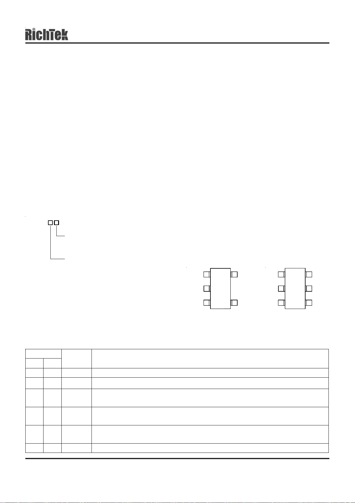
Pin Configurations
(TOP VIEW)
LX
1
VCC
LX
1
6
VCC
Marking Information
For marking information, contact our sales representative
GND
2
FB CE
354
GND
235
FB CE
4
directly or through a RichTek distributor located in your
area, otherwise visit our website for detail.
SOT-25
SOT-26
Functional Pin Description
Pin No.
−−−−XB −−−−XE
1 1 LX Switch Pin. Connect inductor/diode here. Minimize trace area at this pin to reduce EMI.
2 2 GND Ground Pin. Connect directly to local ground plane.
3 3 FB Feedback Pin. Reference voltage is 0.25V. Connect cathode of lowest LED and resistor
4 4 CE Chip Enable Pin. Connect to 1.4V or higher to enable device, 0.4V or less to disable
− 5 OVP Over Voltage Protection Pin. Voltage sensing input to trigger the function of over voltage
5 6 VCC Input Voltage Pin. Must be locally bypass with 1uF capacitor to GND.
Pin Name Pin Function
here. Calculate resistor value according to the formula: R
device.
protection, the trip point is 15.5V. Leave it unconnected to disable this function.
= 0.25/I
FB
LED
OVP
DS9271-07 April 2004 www.richtek.com
1
RT9271
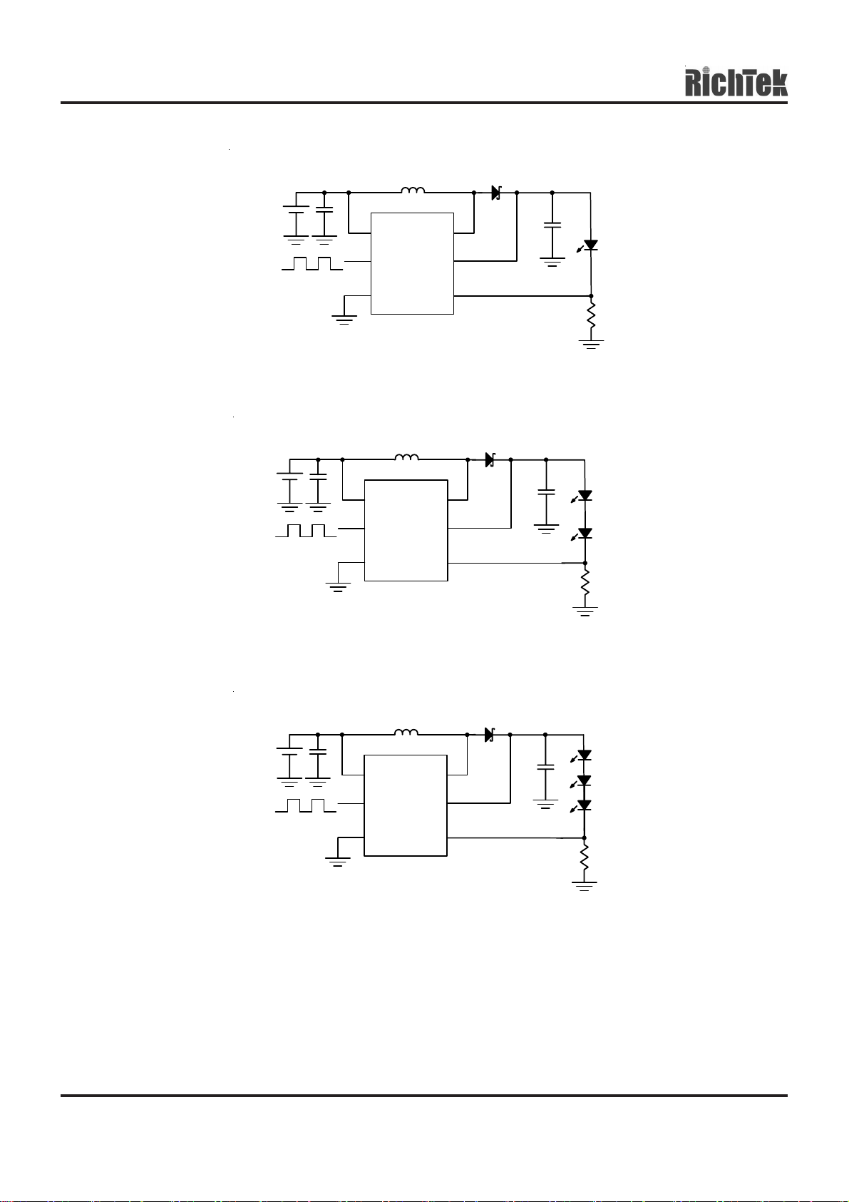
Typical AppIication Circuit
D1
SS0520
V
IN
2.4 to 3.2V
C1
1uF
Dimming
Control
VCC
CE
GND
LX
10uH
LX
OVP
FB
Figure 1. RT9271 Drivers 1 WLED Application Circuit
V
IN
2.4 to 5V
C1
1uF
Dimming
Control
VCC
CE
GND
LX
10uH
LX
OVP
FB
D1
SS0520
C3
1uF
C3
1uF
D2
R2
12Ω
D2
D3
R2
12Ω
Figure 2. RT9271 Drivers 2 Series WLEDs Application Circuit
LX
10uH
VCC
CE
GNDLXFB
V
IN
2.4 to 6V
C1
1uF
Dimming
Control
Figure 3. RT9271 Drivers 3 Series WLEDs Application Circuit
Note : 1. D1 is Schottky diode (SS0520).
2. D2 ~ D4 are the WLED (HT-S91CW-DT) of HARVATEK.
3. LX is the SH4018 series of ABC TAIWAN ELECTRONICS CORP.
OVP
D1
SS0520
C3
1uF
D2
D3
D4
R2
12Ω
DS9271-07 April 2004www.richtek.com
2

RT9271
Recommended Circuits for Driving LEDs
Figure 1 to Figure 3 illustrates the recommended application circuits for driving white LEDs. The series connected
LEDs are driven with identical current to emit uniform luminescence, and the 250mV low reference voltage can minimize
the efficiency loss across the current-sensing resistor. The recommended current setting for driving white LEDs is
10mA to 20mA, and the dimming control can be implemented by toggling CE pin with 60Hz to 1KHz PWM clock. Please
refer to application notes for guidance of component selection and board layout.
Function Block Diagram
FB
CE
OVP
V
REF
0.25V
15.5V
-
+
CHIP
ENABLE
4µA
A1
RAMP
GENERATOR
1.1MHz
OSCILLATOR
COMPARATOR
-
A2
+
R Q
S
DRIVER
+
-
LX
VCC
M1
0.75Ω
GND
Operation
The RT9271 is a constant frequency step-up converter with an internal switch. For excellent line and load regulation,
the current mode control is adopted. The operations of RT9271 can be understood from block diagram clearly. The
oscillator triggers the SET input of SR latch to turn on the power switch M1 at the start of each cycle. A current sense
voltage sum with a stabilizing ramp is connected to the positive terminal of the PWM comparator A2. When this voltage
exceeds the output voltage of the error amplifier A1, the SR latch is reset to turn off the power switch till next cycle
starts. The output voltage of the error amplifier A1 is amplified from the difference between the reference voltage 0.25V
and the feedback voltage. In this manner, if the error amplifiers voltage increases, more current is delivered to the
output; if it decreases, less current is delivered. A 15.5V Zener diode connects from OVP pin to FB pin internally to
provide an optional protection function which prevents LX pin from over-voltage damage. Especially when the case of
the feedback loop broken due to component wear-out or improper connection occurs. The behavior of OVP is to clamp
the output voltage to 15.5V typically. This function is suitable for the applications while driving white LEDs less than 4 in
series.
DS9271-07 April 2004 www.richtek.com
3

RT9271
Absolute Maximum Ratings (Note 1)
Supply Voltage, V
LX, OVP ----------------------------------------------------------------------------------------------------------------- −0.3V to 21V
The Other Pins -------------------------------------------------------------------------------------------------------- −0.3V to 7V
Maximum Junction Temperature ---------------------------------------------------------------------------------- 125°C
Operating Junction Temperature Range ------------------------------------------------------------------------ −40°C to 125°C
Lead Temperature (Soldering, 10 sec.) ------------------------------------------------------------------------- 260° C
Storage Temperature Range --------------------------------------------------------------------------------------- −65° C to 150° C
ESD Susceptibility (Note 2)
HBM ---------------------------------------------------------------------------------------------------------------------- 2kV
MM ------------------------------------------------------------------------------------------------------------------------ 200V
Recommended Operating Conditions(Note 3)
Supply Voltage, V
Electrical Characteristics
(V
= 3.6V, T
CC
System Supply Input
Under Voltage Lock Out UVLO 1.8 2.2 2.3 V
Maximum Output Voltage -- -- 20 V
Supply Current I
Quiescent Current I
Shut Down Current I
Oscillator
Operation Frequency F
Maximum Duty Cycle Dmax 85 90 -- %
Reference Voltage
Feedback Voltage VFB 0.237 0.25 0.263 V
MOSFET
On Resistance of MOSFET Rds(on) 0.5 0.75 1.0 Ω
Current Limit I
Current Limit I
Control and Protection
Shut Down Voltage V
Enable Voltage V
CE Pin Pull Low Current ICE -- 4 6 µA
OVP Threshold (Note 4) OVP 14.5 15.5 20.0 V
Note 1. Stresses beyond those listed under “Absolute Maximum Ratings” may cause permanent damage to the device. These
are stress ratings only, and functional operation of the device at these or any other conditions beyond those indicated in
the operational sections of the specifications is not implied. Exposure to absolute maximum rating conditions for extended
periods may affect device reliability.
Note 2. Devices are ESD sensitive. Handling precaution recommended. The human body model is a 100pF capacitor discharged
through a 1.5kΩ resistor into each pin.
Note 3. The device is not guaranteed to function outside its operating conditions.
Note 4. Floating the OVP pin to disable OVP function.
4
= 25°C, unless otherwise specified.)
A
Parameter Symbol Test Condition Min Typ Max Units
-------------------------------------------------------------------------------------------------- −0.3V to 7V
CC
-------------------------------------------------------------------------------------------------- 2.4V to 6V
CC
V
CC1
V
CC2
V
CC3
0.9 1.1 1.3 MHz
OSC
Normal Operation 800 900 1000 mA
max1
Start up Condition 500 625 750 mA
max2
0.4 0.8 -- V
CE1
-- 0.8 1.4 V
CE2
=6V, Continuously Switching -- -- 2 mA
CC
=6V, FB=1.3V, No Switching 50 90 120 µA
CC
=6V, VCE<0.4V -- 0.1 1 µA
CC
DS9271-07 April 2004www.richtek.com

Typical Operating Characteristics
RT9271
Efficiency vs. VIN (Driving 1 WLED)
92
T
= 25°C
A
91
90
89
88
87
86
85
84
83
82
22.533.54
IO = 20mA
IO = 15mA
VIN (V)
Efficiency vs. VIN (Driving 3 WLEDs)
90
T
= 25°C
A
89
88
87
86
85
84
83
82
81
80
23456
VIN (V)
IO = 20mA
IO = 15mA
Efficiency vs. VIN (Driving 2 WLEDs)
90
T
= 25°C
A
89
88
87
86
85
84
83
82
Refer to Application Circuit Figure 1
Refer to Application Circuit Figure 3
81
80
23456
1.3
Driving 3 WLEDs
= 25°C
T
A
1.2
1.1
1
0.9
0.8
0.7
23456
VIN (V)
Frequency vs. V
VIN (V)
IO = 20mA
IO = 15mA
Refer to Application Circuit Figure 2
IN
VFB vs. Temperature
260
Driving 3 WLEDs
V
= 3.6V
IN
255
250
245
FB
240
235
230
0 1020 30405060 70
Temperature
(°C)
3
2.8
2.6
IN
2.4
2.2
Minimum Input Voltage vs. Temperature
for Delivering Full Brightness
2
20 30 40 50 60 70
VIN vs. Temperature
Temperature
(°C)
3 WLEDs
DS9271-07 April 2004 www.richtek.com
5

RT9271
VIN = 2.4V
V
OUT
(AC)
V
LX
VIN = 2.4V
V
OUT
(AC)
Stability for Driving 1 WLED
Stability for Driving 1 WLED
VIN = 3.2V
V
OUT
(AC)
V
LX
I
IN
100mA/Div
Refer to Application Circuit Figure 1
Time (500 ns/Div)
Stability for Driving 2 WLEDs
I
IN
100mA/Div
Refer to Application Circuit Figure 1
Time (500 ns/Div)
Stability for Driving 2 WLEDs
VIN = 3.6V
V
OUT
(AC)
V
LX
I
VIN = 5.2V
V
OUT
(AC)
V
LX
I
V
LX
I
IN
100mA/Div
Refer to Application Circuit Figure 2
Time (500 ns/Div)
Stability for Driving 2 WLEDs
IN
100mA/Div
Refer to Application Circuit Figure 2
Time (500 ns/Div)
Stability for Driving 3 WLEDs
VIN = 2.4V
V
OUT
(AC)
V
LX
I
IN
100mA/Div
Refer to Application Circuit Figure 2
Time (500 ns/Div)
IN
100mA/Div
Refer to Application Circuit Figure 3
Time (500 ns/Div)
DS9271-07 April 2004www.richtek.com
6

RT9271
VIN = 3.6V
V
OUT
(AC)
V
LX
I
VCE = 2V
VIN = 3V
Stability for Driving 3 WLEDs
IN
Time (500 ns/Div)
Inrush Current for Driving 1 WLED
Frequency = 200Hz
100mA/Div
Stability for Driving 3 WLEDs
VIN = 6.0V
V
OUT
(AC)
V
LX
I
IN
Refer to Application Circuit Figure 3
Inrush Current for Driving 2 WLEDs
Frequency = 200Hz
VCE = 2V
VIN = 3.6V
Time (500 ns/Div)
100mA/Div
Refer to Application Circuit Figure 3
I
IN
V
OUT
VCE = 2V
VIN = 3.6V
I
IN
V
OUT
I
= 730mA
IN(max)
Time (20 us/Div)
Inrush Current for Driving 3 WLEDs
Frequency = 200Hz
I
= 730mA
IN(max)
Time (20 us/Div)
I
IN
V
OUT
Refer to Application Circuit Figure 1
Inrush Current for Driving
Frequency = 200Hz
VCE = 2V
VIN = 3.6V
I
IN
V
OUT
Refer to Application Circuit Figure 3
I
= 730mA
IN(max)
Time (20 us/Div)
3 WLEDs with soft-start
I
= 730mA
IN(max)
Time (20 us/Div)
Refer to Application Circuit Figure 2
Refer to Application Circuit Figure 3
DS9271-07 April 2004 www.richtek.com
7

RT9271
Dimming Control for Driving 3 WLEDs
Frequency = 200Hz
V
CE
V
LX
V
OUT
Time (20 us/Div)
VIN = 3.6V
Refer to Application Circuit Figure 3
DS9271-07 April 2004www.richtek.com
8

Application Information
RT9271
LED Current Control
The RT9271 regulates the LED current by setting the
current sense resistor (R2) connecting to feedback and
ground. The internal feedback reference voltage is 0.25V.
The LED current can be set from following equation easily.
2R =
V25.0
LEDI
In order to have an accurate LED current, precision
resistors are preferred (1% is recommended). The table
for R2 selection is shown below.
R2 Resistor Value Selection
I
(mA) R2 (Ω)
LED
5 49.9
10 24.9
12 21
15 16.5
20 12.4
Recommended Inductance and Rectifier (for Li-Ion cell)
D1
SS0520
C3
1uF
R2
12Ω
D2
D3
D4
V
IN
2.4 to 6V
C1
1uF
PWM signal
LX
10uH
VCC
OVP
CE
GNDLXFB
RT9271
Figure 4. PWM Dimming Control Using the CE Pin
b. Using a DC Voltage
Using a variable DC voltage to adjust the brightness is a
popular method in some applications. The dimming control
using a DC voltage circuit is shown in Figure 5. According
to the Superposition Theorem, as the DC voltage
increases, the voltage contributed to VFB increases and
the voltage drop on R2 decreases, i.e. the LED current
decreases. For example, if the VDC range is from 0V to
2.8V, the selection of resistors in Figure 5 sets dimming
control of LED current from 20mA to 0mA.
Condition Inductance (H) Schottky Diode
2 WLEDs 4.7u~10u SS0520
3 WLEDs 4.7u~10u SS0520
Dimming Control
a. Using a PWM Signal to CE Pin
For controlling the LED brightness, the RT9271 can
perform the dimming control by applying a PWM signal
to CE pin. The average LED current is proportional to the
PWM signal duty cycle. The magnitude of the PWM signal
should be higher than the maximum enable voltage of
CE pin, in order to let the dimming control perform
correctly.
V
IN
2.4 to 6V
C1
1uF
LX
10uH
VCC
OVP
EN
GNDLXFB
RT9271
D1
SS0520
R4
82K
VDC Dimmimg
0 to 2.8V
Figure 5. Dimming Control Using a DC Voltage
C3
1uF
R3
6.8K
R2
12
D2
D3
D4
DS9271-07 April 2004 www.richtek.com
9

RT9271
D1
SS0520
C3
1uF
R6
10KΩ
C6
10nF
D2
D3
D4
R5
1KΩ
R2
12Ω
V
IN
2.4 to 6V
C1
1uF
PWM signal
VCC
EN
GND
RT9271
LX
10uH
LX
OVP
FB
Figure 6. Recommended Soft-Start Circuit
Layout Guide
A full GND plane without gap break.
V
to GND noise bypass – Short and wide connection for the 1µF MLCC capacitor between Pin6 and Pin2.
CC
Minimized LX node copper area to reduce EMI.
Minimized FB node copper area and keep far away from noise sources.
C3
S1
D2
D3
D4
C4
V
IN
C5
+
C1
C2
VCC
R1
L1
D1
LX
S3
Board Layout Example (2-Layer EVB Board)
(Refer to EVB Circuit)
CE
OVP
RT9271
FB
GND
EVB Circuit
S2
R2
10
- Top Layer -
- Bottom Layer -
DS9271-07 April 2004www.richtek.com

Outline Dimension
RT9271
H
D
L
C
b
A
e
Dimensions In Millimeters Dimensions In Inches
Symbol
Min Max Min Max
A 0.889 1.295 0.035 0.051
A1 0.000 0.152 0.000 0.006
B 1.397 1.803 0.055 0.071
b 0.356 0.559 0.014 0.022
C 2.591 2.997 0.102 0.118
D 2.692 3.099 0.106 0.122
B
A1
e 0.838 1.041 0.033 0.041
H 0.080 0.254 0.003 0.010
L 0.300 0.610 0.012 0.024
SOT- 25 Surface Mount Package
DS9271-07 April 2004 www.richtek.com
11

RT9271
H
D
L
C
b
A
e
B
A1
Dimensions In Millimeters Dimensions In Inches
Symbol
Min Max Min Max
A 0.889 1.295 0.035 0.051
A1 0.000 0.152 0.000 0.006
B 1.397 1.803 0.055 0.071
b 0.250 0.559 0.010 0.022
C 2.591 2.997 0.102 0.118
D 2.692 3.099 0.106 0.122
e 0.838 1.041 0.033 0.041
H 0.080 0.254 0.003 0.010
L 0.300 0.610 0.012 0.024
RICHTEK TECHNOLOGY CORP.
Headquarter
5F, No. 20, Taiyuen Street, Chupei City
Hsinchu, Taiwan, R.O.C.
Tel: (8863)5526789 Fax: (8863)5526611
12
SOT- 26 Surface Mount Package
RICHTEK TECHNOLOGY CORP.
Taipei Office (Marketing)
8F-1, No. 137, Lane 235, Paochiao Road, Hsintien City
Taipei County, Taiwan, R.O.C.
Tel: (8862)89191466 Fax: (8862)89191465
Email: marketing@richtek.com
DS9271-07 April 2004www.richtek.com

 Loading...