

Page 1

®
RT9266
Tiny Package, High Efficiency, Step-up DC/DC Converter
General Description
The RT9266 is a compact, high eff iciency, a nd low voltage
step-up DC/DC converter with a n Ada ptive Current Mode
PWM control loop, includes an error amplifier, ramp
generator, comparator , switch pa ss element and driver in
which providing a stable and high ef ficient operation over
a wide range of load currents. It operates in stable
waveforms without external compensation.
The low start-up input voltage below 1V makes RT9266
suitable for 1 to 4 battery cells applications of providing
up to 300mA output current. The 450kHz high switching
rate minimized the size of external components. Besides,
the 17μA low quiescent current together with high
efficiency maintains long battery lifetime.
The output voltage is set with two external resistors. Both
internal 2A switch and driver for driving external power
devices (NMOS or NPN) are provided.
Ordering Information
RT9266
Package Type
E : SOT-23-6
X5 : SOT-89-5
Features
zz
1.0V Low Start-up Input Voltage
z
zz
zz
z High Supply Capability to Deliver 3.3V 100mA with
zz
1 Alkaline Cell
μμ
zz
z 17
μA Quiescent (Switch-off) Supply Current
zz
μμ
zz
z Zero Shutdown Mode Supply Current
zz
zz
z 90% Efficiency
zz
zz
z 450kHz Fixed Switching Frequency
zz
zz
z Providing Flexibility for Using Internal and External
zz
Power Switches
zz
z Small SOT-23-6 & SOT-89-5 Package
zz
zz
z RoHS Compliant and 100% Lead (Pb)-Free
zz
Applications
z PDA
z DSC
z LCD Pa nel
z RF-Tags
z MP3
z Portable Instrument
z Wireless Equipment
Pin Configurations
Lead Plating System
(TOP VIEW)
P : Pb Free
G : Green (Halogen Free and Pb Free)
Note :
Richtek products are :
` RoHS compliant and compatible with the current require-
ments of IPC/JEDEC J-STD-020.
` Suitable for use in SnPb or Pb-free soldering processes.
FB
VDD LX
56
23
EN EXT
SOT-23-6
4
1
GND
EN VDD FB
SOT-89-5
LXGND
45
23
Marking Information
For marking information, contact our sales re presentative
directly or through a Richtek distributor located in your
area.
Copyright 2013 Richtek Technology Corporation. All rights reserved. is a registered trademark of Richtek Technology Corporation.
DS9266-16 June 2013 www.richtek.com
©
1
Page 2
RT9266
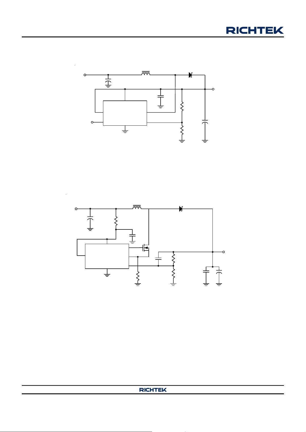
Typical Application Circuit
V
IN
Figure 1. RT9266 T ypical Application for Portable Instruments
3.1V to 5V for 12V
2.8V to 5V for 9V
V
IN
+
C4
100µF
+
C3
100µF
EN
RT9266
EXT GNDLXFB
RVDD
100
3.3 to 10 µH
VDD
L1
4.7µH
L1
C2
1µF
1N5819
D1
1N5819
D1
R1
1.6M/3M
R2
980k/1M
+
C1
100µF
V
OUT
3.3V/5V
EN
CVDD
1µF
RM
0.22
Q1
N MOS
C3
0.1µF
R1
860k/620k
R2
100k
VDD
RT9266
GNDLXFB
EXT
Figure 2. RT9266 High V oltage Applications
C2
1µF
+
C1
100uF
12V/9V
300mA
Copyright 2013 Richtek Technology Corporation. All rights reserved. is a registered trademark of Richtek Technology Corporation.
©
DS9266-16 June 2013www.richtek.com
2
Page 3

RT9266
V
3.3V/5V
L1
EN
+
C3
100µF
3.3 to 10 µH
VDD
RT9266
GNDLXFB
EXT
C2
1µF
V
IN
D1
1N5819
Q1
N MOS
R1
1.6M/3M
R2
980k/1M
+
C1
100µF
V
OUT
3.3V/5V
Figure 3. RT9266 for Higher Current Applications
LX
FB
L1
4.7µH
Q1
N MOS
C8
1µF
C7
1µF
C6
0.1µF
R1
620k
R2
100k
IN
C2
1µF
EXT
C1
1µF
EN
R3
100
VDD
RT9266
GND
C3
10µF
C4
10µF
C5
10µF
V
OUT2
+18V
10mA
V
OUT1
+9V
10mA
V
OUT3
-9V
10mA
Figure 4. RT9266 for Multi-Output Applications
Copyright 2013 Richtek Technology Corporation. All rights reserved. is a registered trademark of Richtek Technology Corporation.
DS9266-16 June 2013 www.richtek.com
©
3
Page 4

RT9266
Test Circuit
I (VIN)
V
IN
A
+
C3
100µF
A
I (VDD)
VDD
EN
RT9266
EXT GNDLXFB
Functional Pin Description
Pin No.
SOT-23-6 SOT-89-5
1 1 EN
2 -- EXT
3 5 GND
Pin Name
L1
10µH
C2
1µF
D1
1N5819
R1
1.6M/3M
R2
980k/1M
C4
102
+
C1
100µF
Pin Function
Chip Enable (Active High).
Output Pin for Driving External N-MOSFET .
Ground.
C5
106
V
OUT
3.3V/5V
4 4 LX Pin for Switching.
5 2 VDD
6 3 FB
Function Block Diagram
VDD
FB
EN
In put Posi tive Powe r Pin of RT9266 .
Feedback Input Pin.
Internal Reference Volt age for the Error Amplifier is 1.25V.
RT9266
Q1
N MOS
R1
1.25V
VDD
R2
Q2
N MOS
-
Loop Control Circuit
+
Over Temp.
Detector
Shut Down
EXT
LX
GND
Copyright 2013 Richtek Technology Corporation. All rights reserved. is a registered trademark of Richtek Technology Corporation.
©
DS9266-16 June 2013www.richtek.com
4
Page 5

RT9266
Absolute Maximum Ratings
z Supply V oltage------------------------------------------------------------------------------------------------------ −0.3V to 7V
z LX Pin Switch Voltage --------------------------------------------------------------------------------------------- −0.3V to 7V
z Other I/O Pin Voltages -------------------------------------------------------------------------------------------- −0.3V to (V
z LX Pin Switch Current --------------------------------------------------------------------------------------------- 2.5A
z EXT Pin Driver Current --------------------------------------------------------------------------------------------- 200mA
z Package Thermal Resista nce
SOT-23-6, θJC------------------------------------------------------------------------------------------------------- 145°C/W
SOT-89-5, θJC------------------------------------------------------------------------------------------------------- 45°C/W
z Operating Junction T emperature -------------------------------------------------------------------------------- 125°C
z Storage T emperature Range ------------------------------------------------------------------------------------- −65°C to +150°C
NOTE:
Absolute Maximum ratings are threshold limit values that must not be exceeded even for a n instant under a ny conditions.
Moreover, such values f or any two items must not be rea ched simulta neously . Operation above these absolute maximum
ratings may cause degradation or permanent da mage to the device. These are stress ratings only a nd do not necessarily
imply functional operation below these limits
+ 0.3V)
DD
Recommended Operating Conditions (1)
z Junction T emperature Range-------------------------------------------------------------------------------------- −40°C to 125°C
z Ambient T emperature Range-------------------------------------------------------------------------------------- −40°C to 85°C
Electrical Characteristics
(VIN = 1.5V, VDD set to 3.3V, Load Current = 0, TA = 25° C, unless otherwise specified)
Parameter Symbol Test Conditions Min Typ Max Unit
Sta rt- UP Vo l t a g e
Operating VDD Range
Shutdown Current I (VIN) I
Switch-off Current I (VDD)
Continuous Switching Current
No Load Curre nt I (VIN) I
Feedback Reference V oltage
Switching Frequency
Maximum Duty
LX ON Resistance
Current Limit Setting
EXT ON Re sistance to VDD
EXT ON Re sistance to GND
V
I
ST
V
V
DD
EN Pin = 0V, VIN = 4.5V
OFF
I
SWITCH OFF
I
SWITCH
NO LOAD
V
F
D
I
LIMIT
VIN = EN = 3.3V, VFB = GND
VIN = 1.5V, V
REF
V
S
V
MAX
V
= 1mA
L
pin voltag e
DD
VIN = 6V
OUT
Clo se Loo p, V DD = 3.3V 1.22 5 1.2 5 1. 27 5 V
= 3.3 V
DD
= 3.3V
DD
V
= 3.3V
DD
= 3.3V
DD
V
= 3.3V
DD
V
= 3.3V
DD
= 3.3V
-- 0.98 1.05 V
2 -- 6 V
-- 0.01 1
-- 17 25
0.4 0.55 0.7 mA
--
75
(2)
--
425 500 575 kHz
85 95 -- %
-- 0.3 1.1
1.6 2
2.6
(3)
-- 5 8.5 Ω
-- 5 8.5
μA
μA
μA
Ω
A
Ω
Copyright 2013 Richtek Technology Corporation. All rights reserved. is a registered trademark of Richtek Technology Corporation.
DS9266-16 June 2013 www.richtek.com
©
5
Page 6

RT9266
Parameter Symbol Test Conditions Min Typ Max Unit
Line Regulation
Load Re gul ation
ΔV
ΔV
EN Pin Trip Level
Tempera ture Stabi lit y for V
Thermal Shutdown Hysteresis
Note :
(1). The device is not guaranteed to function outside its operating conditions.
(2). No Load Current is highly dependent on practical system design and component selection that cannot be covered by
production testing. Typical No Load Current is verified by typical application circuit with recommended components. No
Load Current performance is guaranteed by Switch Off Current and Continuous Switching Current.
(3). Current Limit is guaranteed by design at T
(4). Load Regulation is not tested at production due to practical instrument limitation. Load Regulation performance is
dominantly dependent on DC loop gain and LX ON Resistance that are guaranteed by
Resistance
” tests in production.
OUT
TS
ΔT
VIN = 3. 5 ~ 6V, IL = 1mA
LINE
VIN = 2.5V, IL = 1 ~ 100mA
LOAD
= 3. 3V
V
DD
-- 50 --
SD
-- 10 --
= 25°C.
A
-- 1.5 10 mV/V
0.25
(4)
-- mV/mA
--
0.4 0.8 1.2 V
ppm/°C
°C
“Line Regulation” and “LX ON
Copyright 2013 Richtek Technology Corporation. All rights reserved. is a registered trademark of Richtek Technology Corporation.
6
©
DS9266-16 June 2013www.richtek.com
Page 7
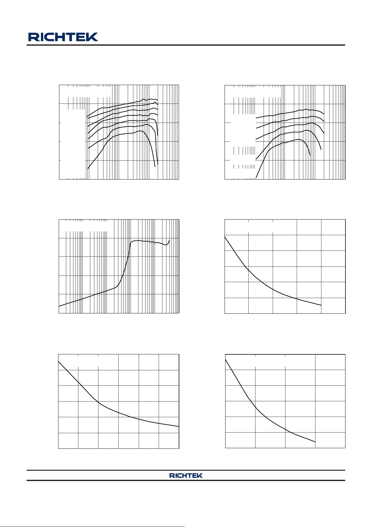
Typical Operating Characteristics
(Refer to Test Circuit)
RT9266
95
V
= 5V, TA = 25°C
OUT
90
V
= 4.5V
IN
V
= 4.0V
IN
85
V
= 3.5V
IN
V
= 3.0V
IN
80
V
= 2.5V
IN
Efficiency (%)
70
V
= 2.0V
IN
75
= 1.5V
V
IN
000 001 010 100 1000
Output Current (mA)
Input Current I(VDD) vs. Output Current
250
V
Efficiency vs . Output Current
= 3V, V
IN
200
μ
150
100
Input Current ( A)
50
OUT
= 5V
Efficiency vs. Output Current
95
V
= 3.3V, TA = 25°C
OUT
90
V
= 3.0V
V
V
IN
IN
IN
= 2.5V
= 2.0V
85
80
Eff iciency (%)
V
= 1.5V
IN
75
70
V
= 1.0V
IN
0.1 1 10 100 1000
Output Current (mA)
Inpu t Curre nt I(VDD) vs. Input Voltage
21
V
= 5V @ no load
OUT
20
μ
19
18
17
Input Current ( A)
16
0
0.01 0.1 1 10 100 1000
Output Current (mA)
Supply Current I(VIN) vs. Input Voltage
180
V
= 5V @ no load
OUT
150
μ
120
90
60
Supply Current ( A) 1
30
0
1.5 2.0 2.5 3.0 3.5 4.0 4.5
Input Voltage (V)
Copyright 2013 Richtek Technology Corporation. All rights reserved. is a registered trademark of Richtek Technology Corporation.
©
15
2.5 3.0 3.5 4.0 4.5 5.0
Input V o lta ge (V)
Supply Current I(VIN) vs. Input Voltage
90
V
= 3.3V @ no load
OUT
80
μ
70
60
50
Supply Current ( A)
40
30
1.5 2 2.5 3 3.5
Input Voltage (V)
DS9266-16 June 2013 www.richtek.com
7
Page 8
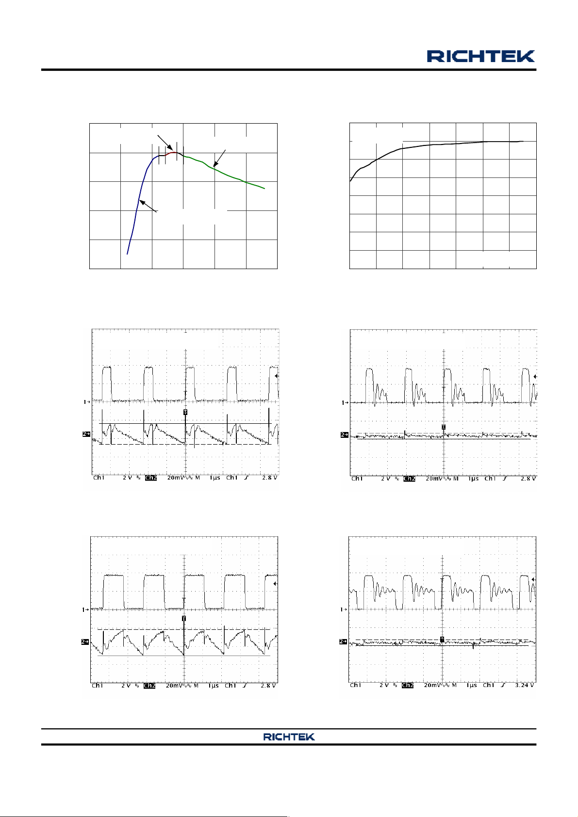
RT9266
Start Up Voltage (V)
Switching Rate Frequency (KHz).
Swichting Frequency vs. VDD Pin Voltage
Switching Frequency vs. VDD Pin Voltage
600
V
IN
500
= 2.4V to 2.8V
V
= 3V to 5.6V
IN
Start Up Voltage vs. Output Current
1.6
V
= 3.3V
OUT
1.4
1.2
400
300
200
V
= 1.2V to 2.2V
IN
Switching Frequency (kHz)
100
0 1 2 3 4 5 6
VDD Pin Voltage (V)
LX & Output Ripple
V
= 1V, V
IN
= 3.3V @ 100mA
OUT
1.0
0.8
0.6
0.4
0.2
0.0
0 30 60 90 120 150 180 210
(In C.R. mode)
Output Current (mA)
LX & Output Ripple
V
= 1V, V
IN
= 3.3V @ 10mA
OUT
Output Ripple LX
Time (1µs/Div)
LX & Output Ripple
V
= 2V, V
IN
Output Ripple LX
Copyright 2013 Richtek Technology Corporation. All rights reserved. is a registered trademark of Richtek Technology Corporation.
©
= 3.3V @ 200mA
OUT
Time (1µs/Div)
Output Ripple LX
Output Ripple LX
V
= 2V, V
IN
Time (1µs/Div)
LX & Output Ripple
= 3.3V @ 10mA
OUT
Time (1µs/Div)
DS9266-16 June 2013www.richtek.com
8
Page 9

RT9266
Output Ripple LX
V
V
IN
= 3V, V
IN
= 2V, V
LX & Output Ripple
= 3.3V @ 200mA
OUT
Time (1µs/Div)
LX & Output Ripple
= 5V @ 200mA
OUT
Output Ripple LX
V
V
IN
IN
LX & Output Ripple
= 3V, V
= 3.3V @ 10mA
OUT
Time (1µs/Div)
LX & Output Ripple
= 2V, V
= 5V @ 20mA
OUT
Output Ripple LX
Time (1µs/Div)
LX & Output Ripple
V
= 3V, V
IN
Output Ripple LX
Copyright 2013 Richtek Technology Corporation. All rights reserved. is a registered trademark of Richtek Technology Corporation.
©
= 5V @ 200mA
OUT
Time (1µs/Div)
Output Ripple LX
Output Ripple LX
V
= 3V, V
IN
Time (1µs/Div)
LX & Output Ripple
= 5V @ 20mA
OUT
Time (1µs/Div)
DS9266-16 June 2013 www.richtek.com
9
Page 10

RT9266
Output Ripple LX
LX & Output Ripple
V
= 4.5V, V
IN
Transient Response
V
= 2V, V
IN
I
OUT
OUT
= 10mA 200mA
= 5V @ 200mA
OUT
Time (1µs/Div)
= 3.3V
Output Ripple LX
LX & Output Ripple
V
= 4.5V, V
IN
Transient Response
V
= 3V, V
IN
I
OUT
OUT
= 10mA 200mA
= 5V @ 20mA
OUT
Time (1µs/Div)
= 3.3V
Output Transient Voltage
Output Transient Voltage
Transient Response
V
= 3V, V
IN
I
OUT
OUT
= 10mA 200mA
Time (50µs/Div)
= 5V
Time (50µs/Div)
Output Transient Voltage
Output Transient Voltage
Transient Response
V
= 4.5V, V
IN
I
= 10mA 200mA
OUT
Time (50µs/Div)
= 5V
OUT
Time (50µs/Div)
Copyright 2013 Richtek Technology Corporation. All rights reserved. is a registered trademark of Richtek Technology Corporation.
©
DS9266-16 June 2013www.richtek.com
10
Page 11
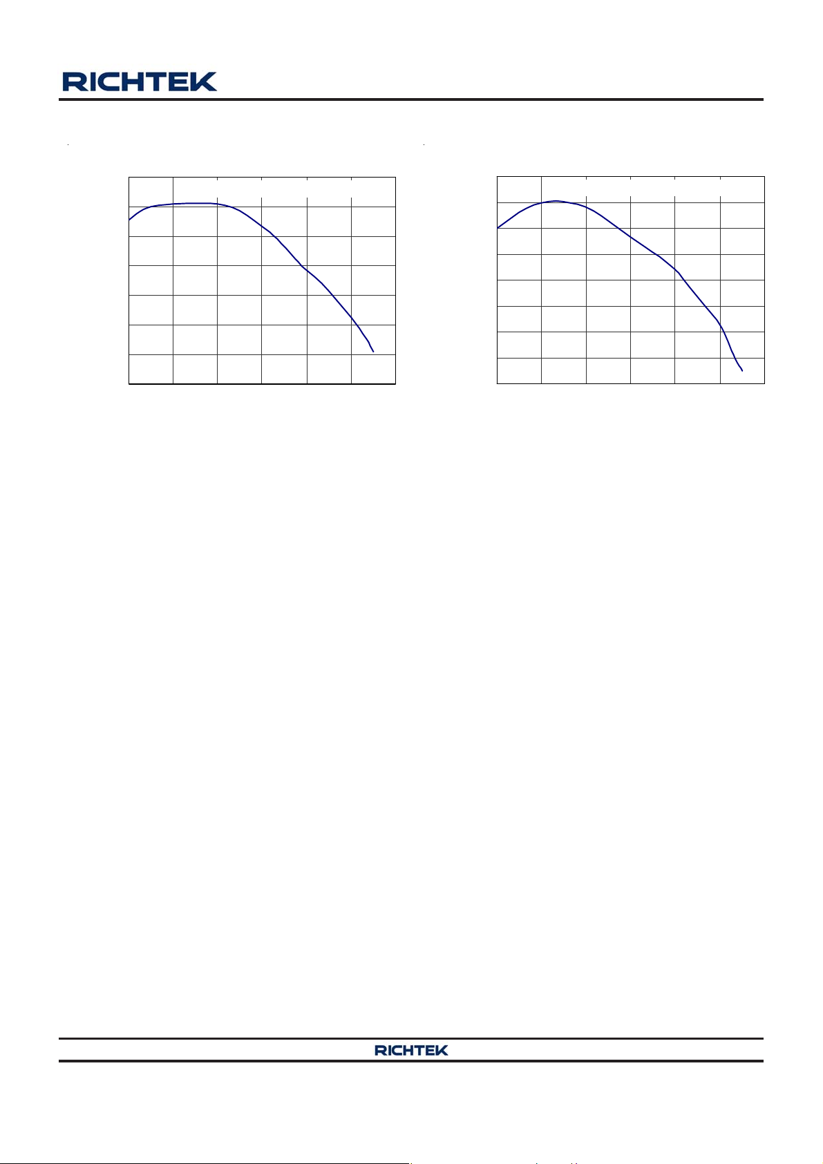
RT9266
Output Voltage vs. Temperature
3.34
3.32
3.3
3.28
3.26
3.24
Output Voltage(V)
3.22
3.2
-40 -10 20 50 80 110 140
V
= 1.8V, V
IN
Temperature
= 3.3V, I
OUT
OUT
(°C)
= 100mA
Output Voltage vs. Temperature
5
4.98
4.96
4.94
4.92
4.9
Output Voltage(V)
4.88
4.86
4.84
-40 -10 20 50 80 110 140
V
= 3V, V
IN
Temperature
OUT
= 5V, I
(°C)
OUT
= 100mA
Copyright 2013 Richtek Technology Corporation. All rights reserved. is a registered trademark of Richtek Technology Corporation.
©
DS9266-16 June 2013 www.richtek.com
11
Page 12

RT9266
Application Information
Output Voltage Setting
Referring to T ypical Application Circuits, the output voltage
of the switching regulator (V
) can be set with Equation
OUT
(1).
R1
V =( 1+ ) 1.25V
×OUT
(1)
R2
Feedback Loop Design
Referring to Typical Application Circuits. The selection of
R1 and R2 based on the trade-off between quiescent
current consumption and interference immunity is stated
below:
z Follow Equation (1)
z Higher R reduces the quiescent current (Path current =
1.25V/R2), however resistors beyond 5MΩ are not
recommended.
z Lower R gives better noise immunity , and is less sensitive
to interference, layout parasitics, FB node le akage, a nd
improper probing to FB pins.
Layout Guide
z A full GND plane without ga p brea k.
z V
to GND noise bypa ss − Short a nd wide connection
DD
for the 1μF MLCC ca pa citor between Pin5 a nd Pin3.
z V
to GND noise bypass − Add a ca pa citor close to L1
IN
inductor, when VIN is not an idea voltage source.
z Minimized FB node copper area a nd keep far away from
noise sources.
z Minimized parasitic capacitance connecting to LX and
EXT nodes, which may cause additional switching loss.
Board Layout Example (2-Layer Board)
(Refer to T ypical Application Circuits Figure 2 for the board)
V
OUT
Prober Parasitics
_
Q
+
z A proper value of feed f orward capa citor parallel with R1
R1
FB Pin
R2
can improve the noise i mmunity of the feedba ck loops,
especially in a n improper layout. An empirical suggestion
is around 0~33pF for feedback resistors of MΩ, and
10nF~0.1μF for feedback resistors of ten s to hundreds
kΩ.
For application s without standby or suspend modes, lower
values of R1 and R2 are preferred. For applications
concerning the current consumption in standby or suspend
modes, the higher values of R1 and R2 are needed. Such
“high impedance feedback loops” are sensitive to any
interference, which require careful layout and avoid a ny
interference, e.g. probing to FB pin.
- Top Layer -
- Bottom Layer -
Copyright 2013 Richtek Technology Corporation. All rights reserved. is a registered trademark of Richtek Technology Corporation.
12
©
DS9266-16 June 2013www.richtek.com
Page 13

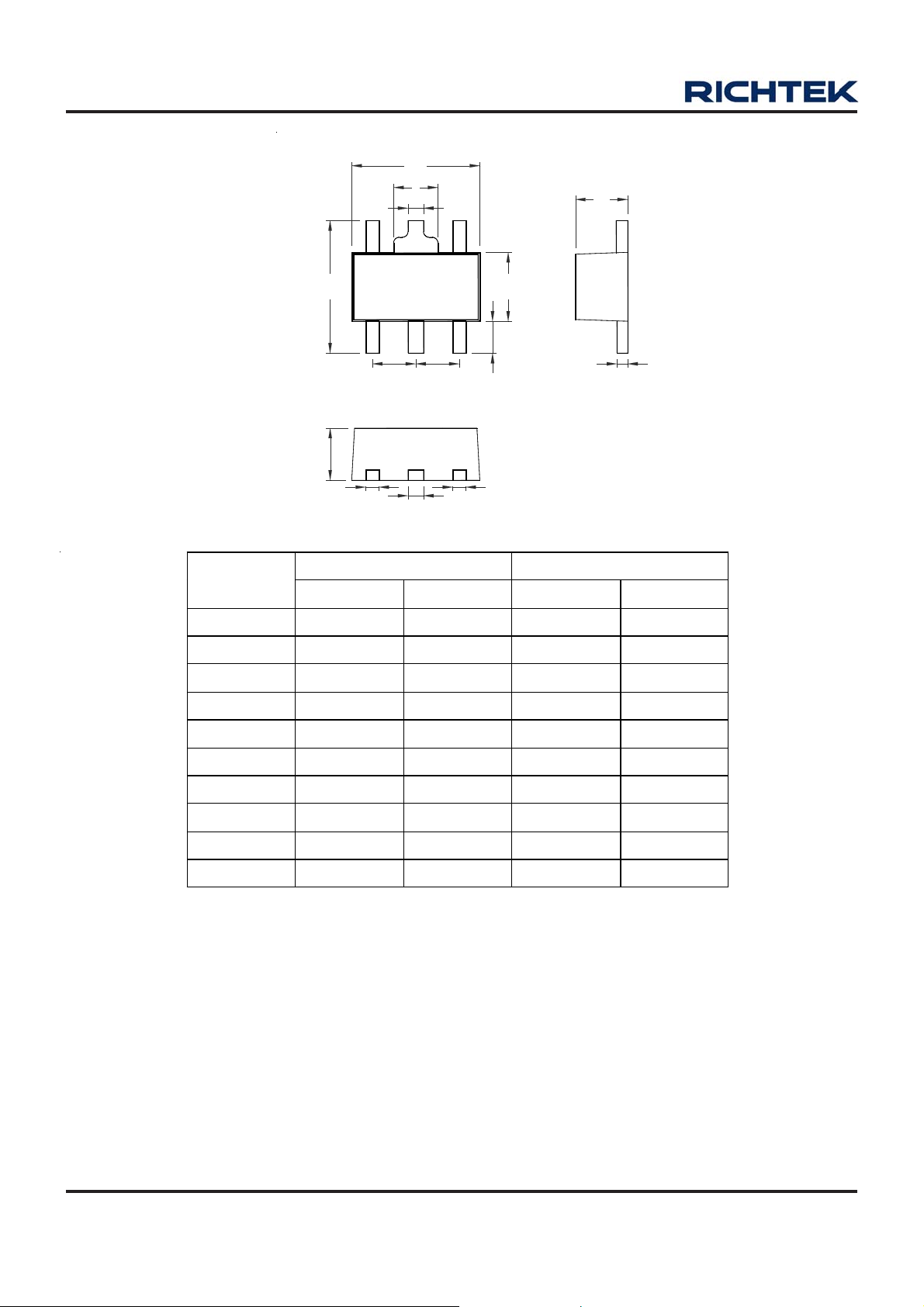
Outline Dimension
RT9266
H
D
L
C
b
A
e
Dimensions In Millimeters Dimensions In Inches
Symbol
Min Max Min Max
A 0.889 1.295 0.031 0.051
A1 0.000 0.152 0.000 0.006
B 1.397 1.803 0.055 0.071
b 0.250 0.560 0.010 0.022
C 2.591 2.997 0.102 0.118
B
A1
D 2.692 3.099 0.106 0.122
e 0.838 1.041 0.033 0.041
H 0.080 0.254 0.003 0.010
L 0.300 0.610 0.012 0.024
SOT-23-6 Surface Mount Package
Copyright 2013 Richtek Technology Corporation. All rights reserved. is a registered trademark of Richtek Technology Corporation.
DS9266-16 June 2013 www.richtek.com
©
13
Page 14
RT9266
D1
D
b1
A
C
e e
A
b1
b
b
B
C1
H
Dimensions In Millimeters Dimensions In Inches
Symbol
Min Max Min Max
A 1.397 1.600 0.055 0.063
b 0.356 0.508 0.014 0.020
B 2.388 2.591 0.094 0.102
b1 0.406 0.533 0.016 0.021
C 3.937 4.242 0.155 0.167
C1 0.787 1.194 0.031 0.047
D 4.394 4.597 0.173 0.181
D1 1.397 1.702 0.055 0.067
e 1.397 1.600 0.055 0.063
H 0.356 0.432 0.014 0.017
5-Lead SOT-89 Surface Mount Package
Richtek Technology Corporation
5F, No. 20, Taiyuen Street, Chupei City
Hsinchu, Taiwan, R.O.C.
Tel: (8863)5526789
Richtek products are sold by description only. Richtek reserves the right to change the circuitry and/or specifications without notice at any time. Customers should
obtain the latest relevant information and data sheets before placing orders and should verify that such information is current and complete. Richtek cannot
assume responsibility for use of any circuitry other than circuitry entirely embodied in a Richtek product. Information furnished by Richtek is believed to be
accurate and reliable. However, no responsibility is assumed by Richtek or its subsidiaries for its use; nor for any infringements of patents or other rights of third
parties which may result from its use. No license is granted by implication or otherwise under any patent or patent rights of Richtek or its subsidiaries.
DS9266-16 June 2013www.richtek.com
14
Page 15

 Loading...