

Datasheet RT9261B-18PB, RT9261B-28GX, RT9261B-28PB, RT9261B-28PX, RT9261B-30GB Datasheet (Richtek) [ru]
...Page 1
VFM Step-Up DC/DC Converter
RT9261B
General Description
The RT9261B Series are VFM Step-up DC/DC converter
ICs with ultra low supply current by CMOS process and
suitable for use with battery-powered instruments.
The RT9261B IC consists of a n oscillator , a VFM control
circuit, a driver transistor (LX switch), a reference voltage
unit, an error a mplifier , resistors for voltage detection, a nd
a LX switch protection circuit. A low ripple a nd high efficiency
step-up DC/DC converter can be constructed with the
RT9261B IC and only three extern al components.
The EN pin enables the circuit to set the standby supply
current at a maximum of 0.5μA.
Ordering Information
RT9261B-
Package Type
B : SOT-23-5
X : SOT-89
Lead Plating System
P : Pb Free
G : Green (Halogen Free and Pb Free)
Output Voltage
15 : 1.5V
16 : 1.6V
:
49 : 4.9V
50 : 5.0V
Note :
Richtek products are :
` RoHS compliant and compatible with the current require-
ments of IPC/JEDEC J-STD-020.
` Suitable for use in SnPb or Pb-free soldering processes.
Features
zz
Minimal Number of External Components (Only an
z
zz
Inductor, a Diode, and a Capacitor)
zz
z Ultra Low Input Current (6.5
zz
z Capable of Supplying 50mA Output Current with
μμ
μA at Switch Off)
μμ
Internal Switch
±±
zz
z
± 2% Output V oltage Accura cy
zz
±±
zz
z Low Ripple and Low Noise
zz
zz
z Low Start-up Voltage, 0.8V at 1mA
zz
zz
z 80% Efficiency with Low Cost Inductor
zz
zz
z +50 ppm/°C Low Temperature-Drift
zz
z SOT-89 and SOT-23-5 Small Packages
zz
z RoHS Compliant and 100% Lead (Pb)-Free
zz
Applications
z Power source for battery-powered equipment
z Power source for ca mera s, ca mcorders, VCRs, PDAs,
pagers, electronic data ban ks, and ha nd-held
communication equipment
z Power source for a pplia nces, which require higher
voltage than that of batteries used in the a ppli ances
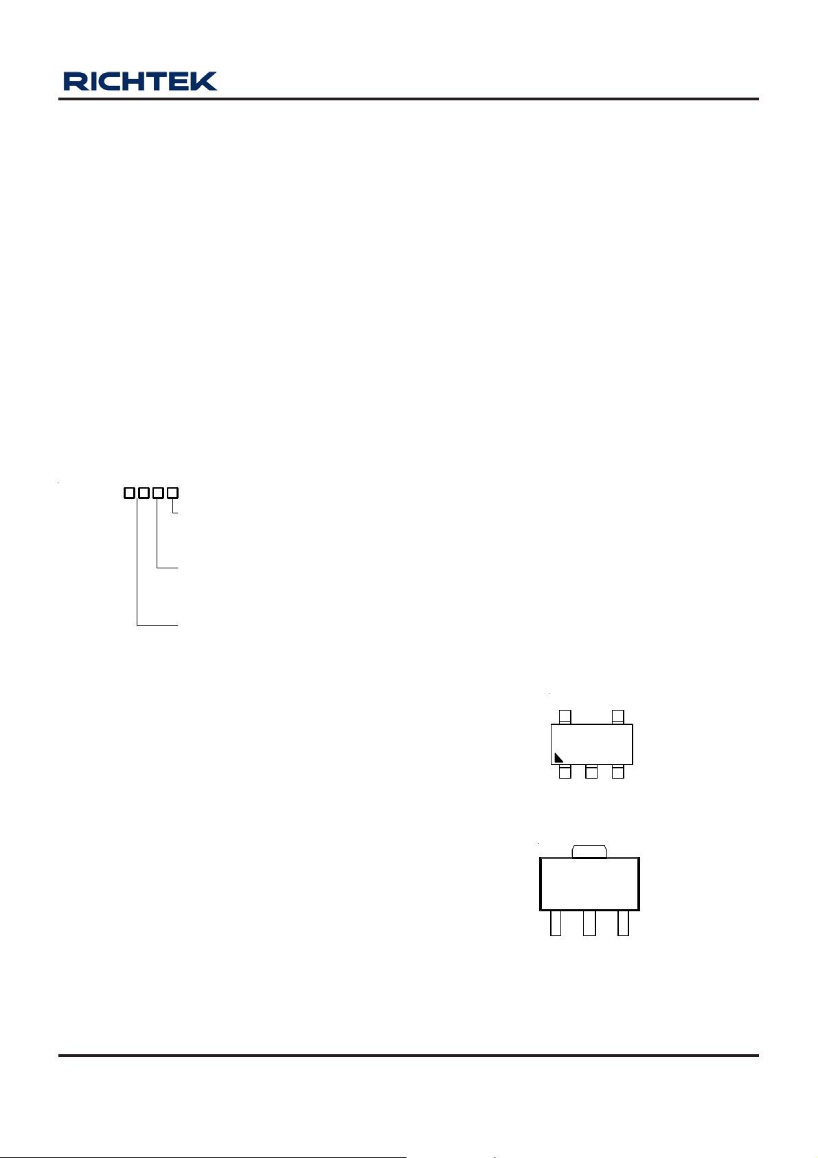
Pin Configurations
(TOP VIEW)
LX GND
5
EN VOUT NC
SOT-23-5
4
23
Marking Information
For marking information, conta ct our sales representative
directly or through a Richtek distributor located in your
area.
DS9261B-16 April 2011 www.richtek.com
123
VOUT
GND
(TAB)
LX
SOT-89
1
Page 2

RT9261B
T ypical Application Circuit
V
IN
V
IN
* L1 ranges from 27μH to 120μH
L1
L1
1N5819
RT9261B
1N5819
RT9261B
LX
EN
D1
GND
D1
GND
VOUTLX
VOUT
+
C
OUT
22µF
+
C
OUT
22µF
V
V
OUT
OUT
Functional Pin Description
Pin No.
SOT-23-5 SOT-89
1 -- EN Chip Enable (Act ive High).
2 2 VOUT Output Voltage.
3 -- NC No Internal Connection.
4 1 GND Ground.
5 3 LX Pin for Switching.
Pin Name Pin Function
Function Block Diagram
LX
LXSW
GND
VLX Limiter
Buffer
OSC 190k H z
Chip Enable
+
Error
Amplifier
V
REF
VOUT
EN
DS9261B-16 April 2011www.richtek.com
2
Page 3
RT9261B
Absolute Maximum Ratings
z Output V oltage ------------------------------------------------------------------------------------------------------ 8V
z LX Pin V oltage------------------------------------------------------------------------------------------------------- 8V
z EN Pin Voltage
z LX Pin Output Current --------------------------------------------------------------------------------------------- 400mA
z Power Dissipation, P
SOT-89 ---------------------------------------------------------------------------------------------------------------- 0.5W
SOT-23-5-------------------------------------------------------------------------------------------------------------- 0.25W
z Pack age Thermal Resistance
SOT-89, θJC---------------------------------------------------------------------------------------------------------- 100°C/W
SOT -89, θJA---------------------------------------------------------------------------------------------------------- 300°C/W
SOT-23-5, θJA-------------------------------------------------------------------------------------------------------- 250° C/W
z Operating T emperature Range ----------------------------------------------------------------------------------- −20 to +85°C
z Storage T emperature Range -------------------------------------------------------------------------------------- −65°C to 150°C
z Lead T emperature (Soldering, 10 sec.) ------------------------------------------------------------------------ 260°C
Notes: (1) Applica ble to RT9261B-xxCB
(1)
---------------------------------------------------------------------------------------------------- −0.3 to V
@ TA = 25°C
D
OUT
+0.3V
Electrical Characteristics (Refer to Figure 1)
Parameter Symbol Test Conditions Min Typ Max Unit
Output Voltage Accuracy ΔV
Input Voltage VIN -- -- 7 V
Start-up Voltage VST I
Hold-on Voltage VHO I
Input Current 1
Input Current 2
and I2)
I
1
(1) (2)
V
LX Switching Current I
LX Leakage Current I
Maximum Oscillator Frequency F
Oscillator Duty Cycle D
Efficiency -- 80 -- %
VLX Voltage Limit LX switch on 0.65 0.8 1.0 V
-2 -- +2 %
OUT
= 1mA, VIN: 0 → 2V -- 0.8 1 V
OUT
= 1mA, VIN: 2 → 0V 0.7 -- -- V
OUT
V
in continuous
IN
switching
in switch off condition -- 6.5 10 μA
OUT
V
SWITCHING VLX
LEAKAGE
MAX
OSC
VLX = 6V -- -- 0.5 μA
On (VLX “L”) side
in no load
IN
= 0.4V
V
= 2.5V to 5V 140 190 240 kHz
OUT
V
= 1.5V to 2.4V 140 190 320 kHz
OUT
V
≤ 3.5V
OUT
3.5V < V
V
≤ 3.5V
OUT
3.5V < V
V
≤ 3.5V
OUT
3.5V < V
V
= 2.5V to 5V 65 75 85 %
OUT
= 1.5V to 2.4V 6 0 70 80 %
V
OUT
(1)
-- 24 36
(2)
OUT
OUT
OUT
≤ 5V
≤ 5V
≤ 5V
-- 36 45
(1)
-- 18 36 Input C urrent 3 (guaranteed by
(2)
(1)
-- 20 45
120 -- --
(2)
160 -- --
μA
μA
mA
Notes:
= 1.8V, VSS = 0V, I
(1) V
IN
= 3V, VSS = 0V, I
(2) V
IN
DS9261B-16 April 2011 www.richtek.com
= 1mA, Topt = 25°C, and use External Circuit of Typical Application
OUT
= 1mA, Topt= 25°C, and External Circuit of Typical Application
OUT
3
Page 4

RT9261B
Electrical Characteristics (Refer to Figure 2)
Parameter Symbol Test Conditions Min Typ Max Unit
Ou tput Voltage Accuracy ΔV
−2 -- +2 %
OUT
Input Voltage VIN -- -- 7 V
Start-up Voltage VST I
Hold-on Voltage VHO I
= 1m A, VIN: 0 → 2V -- 0.8 1 V
OUT
= 1m A, VIN: 2 → 0V 0.7 -- -- V
OUT
Efficiency -- 80 -- %
V
in continuou s
Input Current 1
Input Current 2
I
and I2)
1
(1) (2)
V
LX Switching Current I
LX Leakage Current I
V
SWITCHING
LEAKAGE
IN
switching 3.5V < V
OUT
in no load
IN
VLX = 0.4V
VLX = 6V -- -- 0.5 μA
EN “H” Level VIN = V
EN “L” L evel VIN = V
EN “H” Input Current EN = V
V
≤ 3.5V
OUT
in switch off condition -- 6.5 10 μA
V
≤ 3.5V
OUT
3.5V < V
V
≤ 3.5V
OUT
3.5V < V
* 0.9
OUT
* 0.9 -- -- 0.2 V
OUT
-- -- 0.5 μA
OUT
(1)
-- 24 36
(2)
OUT
OUT
OUT
≤ 5V
(1)
≤ 5V
(1)
≤ 5V
-- 36 45
-- 18 36 Input Current 3 (guaranteed by
(2)
-- 20 45
120 -- --
(2)
160 -- --
0. 4 x
V
OUT
-- -- V
μA
μA
mA
EN “ L” Input Current EN = 0V −0.5 -- -- μA
V
= 2.5V to 5V 140 190 240 kHz
Maximum Oscillator Frequency F
Oscillator Duty Cycle D
MAX
On (VLX “L”) side
OSC
OUT
= 1.5V to 2.4V 140 190 320 kHz
V
OUT
V
= 2.5V to 5V 65 75 85 %
OUT
= 1.5V to 2.4V 60 70 80 %
V
OUT
VLX Voltage Limit LX switch on 0.65 0.8 1.0 V
Notes:
= 1.8V, VSS = 0V, I
(1) V
IN
= 3V, VSS = 0V, I
(2) V
IN
4
= 1mA, Topt = 25°C, and use External Circuit of Typical Application
OUT
= 1mA, Topt= 25°C, and External Circuit of Typical Application
OUT
DS9261B-16 April 2011www.richtek.com
Page 5

Typical Operating Characteristics
RT9261B
Start-up/Hold-on Voltage v s. Output Current
2.5
2
1.5
V
start
1
V
0.5
0
Start-up/Hold-on Voltage Vstart/Vhold (V )1
hold
V
= 3.3V
OUT
L = 47μH
0 30 60 90 120 150 180
Output Current (mA)
Output Current vs. Ripple Voltage
300
250
200
150
100
50
Ripple Voltage (mVp-p) 1
0
0 50 100 150 200
1.5V
1.0V
Output Current (mA)
2.5V
2.0V
V
= 3.3V
OUT
C
= 20μF
OUT
L = 47μH
3.0V
Output Voltage vs. Output Current
4.0
3.5
3.0
2.5
2.0
1.5
1.0
Output Voltage (V) 1
0.5
0.0
0 50 100 150 200
1.0V
1.5V
V
L = 47μH
Output Current (mA)
Output Current vs. Ripple Voltage
90
80
70
60
50
40
30
20
Ripple Voltage (mVp-p)1
10
0
0 50 100 150 200
1.0V
1.5V
Output Current (mA)
3.0V
V
C
L = 47μH
2.0V
OUT
OUT
OUT
3.0V
2.5V
= 3.3V
2.0V
2.5V
= 3.3V
= 68μF
Output Current vs. Ripple Voltage
25
20
15
10
5
Ripple Voltage (mVp-p)1
0
0 50 100 150 200
2.0V
1.5V
2.5V
1.0V
Output Current (mA)
V
OUT
C
OUT
L = 47μH
3.0V
= 3.3V
= 170μF
90
80
70
60
50
40
30
Efficiency (%)1
20
10
0
Efficiency vs. output Current
3.0V
2.5V
1.0V
0 50 100 150 200
1.5V
Output Current ( mA)
2.0V
V
= 3.3V
OUT
L = 47μH
DS9261B-16 April 2011 www.richtek.com
5
Page 6

RT9261B
Start-up/Hold-on Voltage vs. Output Current
2.5
2
1.5
V
start
1
V
0.5
0
Start-up/Hold-on Voltage Vstart/Vhold (V )1
hold
V
= 3.3V
OUT
L = 100μH
0 20406080100120
Output Current (mA)
Output Current vs. Ripple Voltage
300
250
200
150
100
50
Ripple Voltage (mVp-p) 1
0
0 50 100 150 200
1.5V
1.0V
Output Current (mA)
2.0V
3.0V
V
= 3.3V
OUT
C
= 20μF
OUT
L = 100μH
2.5V
Output Voltage vs. Output Current
4.0
3.5
3.0
2.5
2.0
1.5
1.0
Output Voltage (V) 1
0.5
0.0
0 50 100 150 200
1.5V
1.0V
2.0V
V
OUT
L = 100μH
Output Current (mA)
Output Current vs. Ripple Voltage
90
80
70
60
50
40
30
20
1.0V
Ripple Voltage (mVp-p) 1
10
0
0 50 100 150 200
1.5V
Output Current (mA)
2.0V
V
C
L = 100μH
OUT
OUT
3.0V
2.5V
= 3.3V
2.5V
3.0V
= 3.3V
= 68μF
Output Current vs. Ripple Voltage
18
16
14
12
10
8
6
4
Ripple Voltage (mVp-p) 1
2
0
2.0V
1.0V
1.5V
0 50 100 150 200
Output Current (mA)
2.5V
V
OUT
C
OUT
L = 100μH
3.0V
= 3.3V
= 170μF
100
90
80
70
60
50
40
Efficiency (%) 1
30
20
10
0
Efficiency vs. output Current
3.0V
1.0V
1.5V
0 50 100 150 200
2.0V
Output Current (mA)
2.5V
V
= 3.3V
OUT
L = 100μH
DS9261B-16 April 2011www.richtek.com
6
Page 7

Outline Dimension
RT9261B
H
D
L
C
b
A
e
Dimensio ns In Millim eters Dimensions In Inches
Symbol
Min Max Min Max
A 0.889 1.295 0.035 0.051
A1 0.000 0.152 0.000 0.006
B 1.397 1.803 0.055 0.071
b 0.356 0.559 0.014 0.022
C 2.591 2.997 0.102 0.118
D 2.692 3.099 0.106 0.122
B
A1
e 0.838 1.041 0.033 0.041
H 0.080 0.254 0.003 0.010
L 0.300 0.610 0.012 0.024
SOT-23-5 Surf ace Mount Package
DS9261B-16 April 2011 www.richtek.com
7
Page 8

RT9261B
D
D1
A
C
B
C1
e
e
H
A
b
b1
Dimensions In Millimeters Dimension s In Inches
Symbol
Min Max Min Max
A 1.397 1.600 0.055 0.063
b 0.356 0.483 0.014 0.019
B 2.388 2.591 0.094 0.102
b1 0.406 0.533 0.016 0.021
C 3.937 4.242 0.155 0.167
b
C1 0.787 1.194 0.031 0.047
D 4.394 4.597 0.173 0.181
D1 1.397 1.753 0.055 0.069
e 1.448 1.549 0.057 0.061
H 0.356 0.432 0.014 0.017
3-Lead SOT-89 Surface Mount
Richtek Technology Corporation
Headquarter
5F, No. 20, Taiyuen Street, Chupei City
Hsinchu, Taiwan, R.O.C.
Tel: (8863)5526789 Fax: (8863)5526611
Information that is provided by Richtek Technology Corporation is believed to be accurate and reliable. Richtek reserve s the right to make any change in circuit design,
specification or other related things if necessary without notice at any time. No third party intellectual property infringement of the applications should be guaranteed
by users when integrating Richtek products into any application. No legal responsibility for any said applications is assumed by Richtek.
8
Richtek Technology Corporation
Taipei Office (Marketing)
5F, No. 95, Minchiuan Road, Hsintien City
Taipei County, Taiwan, R.O.C.
Tel: (8862)86672399 Fax: (8862)86672377
Email: marketing@richtek.com
DS9261B-16 April 2011www.richtek.com
Page 9

 Loading...