RICHTEK RT9224CS Datasheet

RT9224
5-Bit Programmable Synchronous PWM Buck Converter
Controller and Output Voltage Monitor
General Description
The RT9224 is a high speed switching controller
designed for use in synchronous DC/DC buck
converter for modern CPUs. The regulated output
voltage is digitally programmable from 1.3V to 3.5V
by a 5-bit DAC which provides initial accuracy of
±1%. The RT9224 drives two external N-channel
MOSFETs, providing high efficiency and eliminating
the need for high cost P-channel devices. It senses
the output current across the on-resistance of the
upper N-channel MOSFET and provides an
adjustable current limit without external sense
resistor.
RT9224 monitors the output voltage and provides
the output signal for power-good and over-voltage
protection. The switching controller drivers two N-
MOSFETs at 200kHz frequency and provides an
optimal solution for size, efficiency and cost in any
application circuits. The high switching frequency
cooperating with a high speed error amplifier
maintains a fast response to the dynamic load of
modern CPUs.
Ordering Information
RT9224
Package type
S : SOP-20
Operating temperature range
C: Commercial standard
Features
z
Compatible with HIP6004B
z
Simple Voltage-mode PWM Control with Buck
Rectification
z
±1% DAC Output Voltage Accuracy
z
5-Bit Digital-to-Analog Output Voltage Range
from 1.3 V to 3.5V
z
Fast Transient Response and Excellent Output
Voltage Regulation
z
Fault Protection for Over-voltage and Over-
current
z
Power-good Output Voltage Monitor
z
Fixed 200kHz Switching Frequency
Applications
Power Supply for Pentium, Pentium ProTM,
z
Pentium II
Alpha
Low-voltage Distributed Power Supplies
z
High Power 5V to 1.3V~3.5V Switching Regulator
z
TM
TM
, PowerPCTM, K6TM, 6x86TM, and
Microprocessors
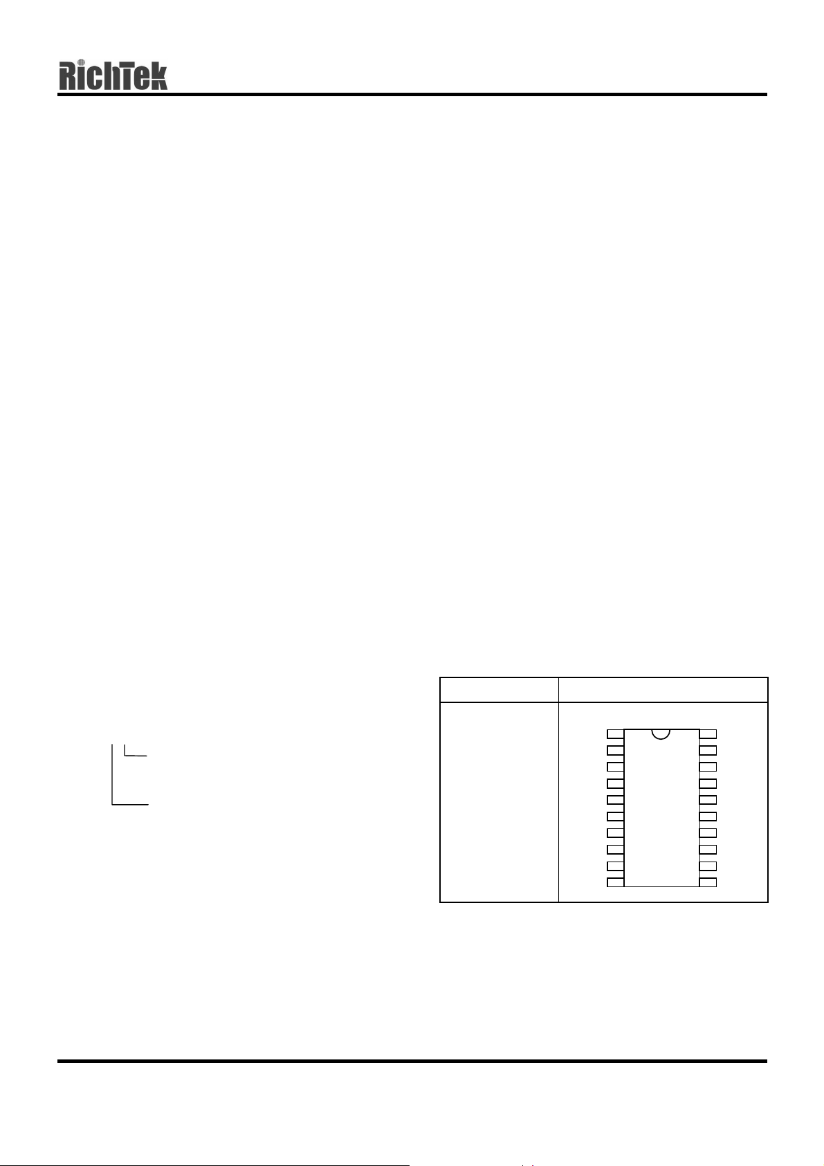
Pin Configurations
Part Number Pin Configurations
RT9224CS
(Plastic SOP-20)
VSEN
OCSET
SS
VID0
VID1
VID2
VID3
VID4
NC
FB
TOP VIEW
1
2
3
4
5
6
7
8
9
10
20
19
18
17
16
15
14
13
12
11
NC
OVP
VCC
LGATE
PGND
BOOT
UGATE
PHASE
PGOOD
GND
DS9224-04 July 2001 www.richtek-ic.com.tw
1

RT9224
Absolute Maximum Ratings
Supply Voltage +15V
z
Boot Voltage +15V
z
Input, Output or I/O Voltage GND – 0.3V to Vcc + 0.3V
z
Storage Temperature Range -65°C ~150°C
z
Package Thermal Resistance
z
SOP-20,θ
JA
Recommended Operating Conditions
87°C/W
Supply Voltage, V
z
Ambient Temperature Range 0°C to 70°C
z
Junction Temperature Range 0°C to 125°C
z
CC
+12V±10%
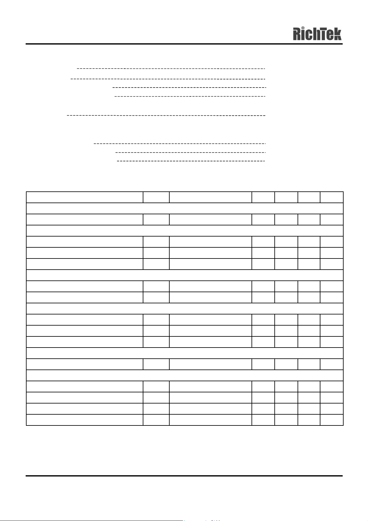
Electrical Characteristics
(T
= 25°C, recommended operating conditions, unless otherwise specified)
A
Parameter Symbol Test Conditions Min Typ Max Units
VCC Supply Current
Nominal Supply
I
CC
UGATE and LGATE Open
Power-On Reset
VCC Rising Threshold
VCC Falling Threshold
Rising V
OCSET
Threshold
V
OCSET
V
OCSET
= 4.5V
= 4.5V
Oscillator
Free Running Frequency 170 200 230
Ramp Amplitude
∆V
OSC
Reference and DAC
DAC (VID0 – VID4) Input Low Voltage -- -- 0.8
--
3--mA
-- 9.5 -- V
-- 7.5 -- V
-- 1.6 -- V
-- 1.9 --
KHz
V
P-P
V
DAC (VID0 – VID4) Input High Voltage 2.0 -- --
DACOUT Voltage Accuracy -1.0 -- +1.0
V
%
Error Amplifier
DC Gain -- 65 --
dB
Gate Drivers
UGATE Source
UGATE Sink
LGATE Source
LGATE Sink
R
UGATEVBOOT
R
UGATEVUGATE
I
LGATE
R
LGATEVLGATE
VCC = 12V, V
- V
- V
= 1V
PHASE
PHASE
LGATE
= 12V
= 1V
= 6V
-- 8 --
-- 5 --
-- 500 --
-- 5 --
Ω
Ω
mA
Ω
To be continued
www.richtek-ic.com.tw DS9224-04 July 2001
2

Protection
RT9224
Parameter Symbol Test Conditions Min Typ Max Units
Over-voltage Trip (VSEN/DACOUT) -- 115 120
OCSET Current Source
OVP Sourcing Current
Soft-Start Current
I
OCSETVOCSET
I
OVP
I
SS
V
SEN
VSS = 1.5V
= 4.5V
= 5.5V, V
OVP
= 0V
167 200 233
60 -- --
-- 10 --
Power Good
Upper Threshold (VSEN/DACOUT) VSEN Rising 106 -- 114
Lower Threshold (VSEN/DACOUT) VSEN Falling 89 -- 96
Hysteresis (VSEN/DACOUT) Upper and Lower Threshold -- 2 --
PGOOD Voltage Low
V
PGOODIPGOOD
= -5mA
-- 0.5 --
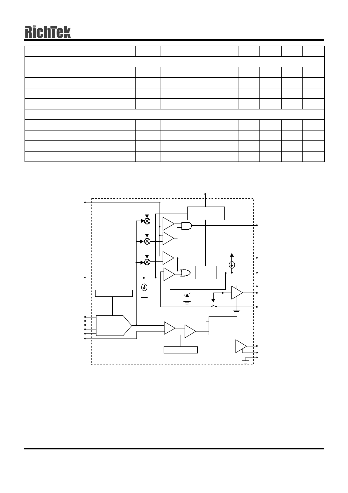
Function Block Diagram
VCC
VSEN
OCSET
REFE RENCE
110%
90%
115%
200µA
+
_
+
_
OVER-
VOLTAGE
+
_
+
_
OVER-
CURRENT
4. 5V
POWER-ON
RESET (POR)
SOFT-
START
PGOOD
OVP
10µA
SS
BOOT
UGATE
%
µA
mA
µA
%
%
%
V
VID0
VID1
VID2
VID3
VID25
FB
DS9224-04 July 2001 www.richtek-ic.com.tw
TTL D/A
CONVERTER
(DAC)
DACO UT
ERRO R
AMP
+
OSCILLATOR
PWM
COMPARATOR
+
_
_
INHIB IT
GATE
CONTROL
LO GIC
PWM
PHASE
LG ATE
PGND
GND
3
 Loading...