RT9223
5-Bit Programmable Synchronous PWM
Buck Converter Controller
General Description
The RT9223 is a high efficiency synchronous
switching regulator for modern CPU application. The
output is controlled by a 5-bit DAC programmed from
1.3V to 2.05V in 0.05V steps and from 2.1V to 3.5V
in 0.1V increments.
The switching controller drivers two N-MOSFETs at
200KHz frequency and provides an optimal solution
for size, efficiency and cost in any application
circuits. The controller also offers integrated
functions including PGOOD, output enable, over-
voltage, internal digital-count soft start, and current-
limiting protection in one chip.
Ordering Information
RT9223
Package type
S : SOP-20
Operating temperature range
C: Commercial standard
Features
z
High Efficiency Synchronous N-MOSFET
Driver Operating at 200KHz
z
1.3V ~ 2.05V (0.05V steps) and 2.1V ~ 3.5V
(0.1V steps) Output Voltage
z
Enable Input, PGOOD Output, OVP, and
Current-limiting Protection
z
Internal Digital-count Soft Start
Applications
Power Supply for Pentium ProTM, PowerPCTM,
z
TM
K6
, 6x86TM, and AlphaTM Microprocessors
High-power 5V to 3.xV DC-DC Regulators
z
Low-voltage Distributed Power Supplies
z
Programmable Step-down Power Supplies
z
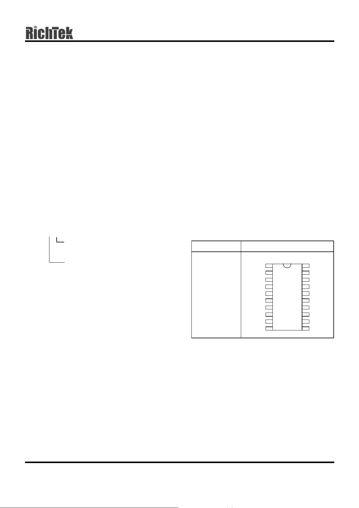
Pin Configurations
Part Number Pin Configurations
DH
NC
TOP VIEW
1
2
3
4
5
6
7
8
9
10
20
19
18
17
16
15
14
13
12
11
VID0
VID1
VID2
VID3
VID4
VSEN
SHDN
BSTH
BSTL
DL
RT9223CS
(Plastic SOP-20)
GND
VCC
OVP
PGOOD
CSN
CSP
PGNDH
PGNDL
DS9223-07 May 2001 www.richtek-ic.com.tw
1

RT9223
Absolute Maximum Ratings
VCC to GND -0.3 to +5.5V
z
PGND to GND ± 0.3V
z
BST to GND -0.3 to +14V
z
Ambient Temperature Range 0 to +70°C
z
z Junction Temperature Range 0 to +125°C
z Storage Temperature Range -65 to +150°C
z Lead Temperature (Soldering, 10 sec.) 300°C
z Package Thermal Resistance
SOP-20, θ
JA
Electrical Characteristics
87°C/W
(VCC = 5V; GND = 0V; PGNDH = PGNDL = 0V; VSEN = VOUT; 0mV < (V
CSP-VCSN
) < 60mV; TA = 25°C)
Parameter Symbol Test Conditions Min Typ Max Units
Switching Section
Output Voltage
Supply Voltage
Supply Current
Load Regulation
Line Regulation
V
OUT
V
CC
I
CC
∆V
LOADIO
∆V
LINE
IO = 2A
VCC 4.3 -- 5.5 V
= 0.8A to 15A
VCC = 4.75V to 5.25V -- 0.5 -- %
-- (1) -- --
-- 2 5 mA
-- 1 -- %
Power On Reset Trip Point VCC Rising -- 4.2 --
Current Limit Voltage
V
LIMIT
V
CSP
- V
CSN
65 75 85
Oscillator Frequency 170 200 230
Oscillator Max Duty Cycle
DH Source
DH Sink
DL Source
DL Sink
D
MAX
V
BSTH
V
DH
V
BL
V
DL
- V
- V
– V
- V
DH
PGNDH
= 5V
DL
PGNDL
= 1V
= 1V
= 1V
90 95 --
-- 4.5 --
-- 3.5 --
-- 1 --
-- 2 --
OVP Threshold Voltage 114 120 122
V
mV
KHz
%
Ω
Ω
A
Ω
%
OVP Source Current
I
OVP
V
OVP
= 3.0V
Power Good Threshold Voltage VSEN Rising 87 -- 115
10 -- --
mA
%
Note: (1) See output voltage table.
www.richtek-ic.com.tw DS9223-07 May 2001
2

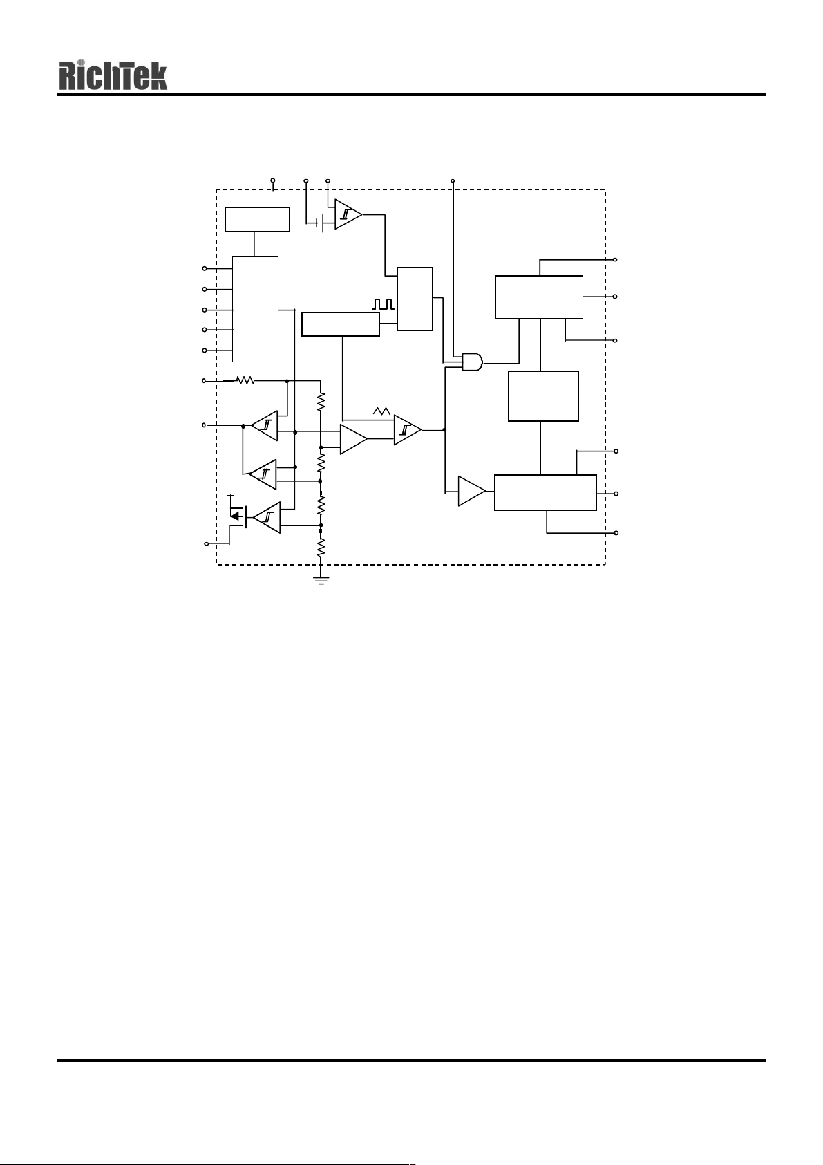
Function Block Diagram
VCC
1. 25 V REF
VID4
VID3
VID2
VID1
VID0
DAC
CSN
CSP
_
+
70mV
OSCILLATOR
CURRENT LI MI T
R
Q
S
SHDN
LEVEL SHIFT
AND DRI VER
RT9223
BSTH
DH
PGNDH
VSEN
PGOOD
OVP
OPEN
DRAIN
VCC
SHOOT-
200KHz
+
_
+
_
+
_
+
_
ERRO R AMP
GND
_
+
THROUGH
CONTROL
DRIVER
BSTL
DL
PGNDL
DS9223-07 May 2001 www.richtek-ic.com.tw
3
 Loading...