

RT9221
Programmable Synchronous PWM Buck Converter with
1.5V/2.5V Dual Low Dropout Linear Regulator Controller
General Description
The RT9221 integrates a PWM controller and two
low-dropout linear regulators into a single chip. The
PWM controller provides the CPU core voltage
controlled by a 5-bit DAC and the linear section
regulates power for GTL bus, clock driver or other
circuits on motherboards. The PWM controller
provides an adjustable Intel-compatible 1.3V~3.5V
output voltage. The synchronous N-MOSFET driver
with 200 KHz switching frequency optimizes the
efficiency, device size, and cost built-in over–voltage
and current-limiting protection prevent the CPU from
damage. Power-good signal is sent when the core
voltage is within ±10% of the setting point.
The linear section is a low dropout regulator which
drives low cost NPN transistors to supply the 1.5V
and 2.5V regulated output power.
Ordering Information
Features
z
Provides 3 Regulated Voltages
z
N-MOSFET Driver for High Efficiency
Switching Section
z
Power-good, Over-voltage, and Current-
limiting Protection for Switching Section
z
1.5V and 2.5V Fixed Output Voltage for Linear
Section
z
Linear Section Uses Low Cost NPN Transistor
as Power Device
z
TTL-compatible 5-bit DAC Core Output
Voltage
Applications
Power Supply for Pentium, Pentium ProTM,
z
Pentium II
Alpha
High-power 5V to 3.xV DC-DC Regulators
z
Low-voltage Distributed Power Supplies
z
Programmable Power Supplies
z
TM
TM
, Power PCTM, K6TM, 6×86TM, and
Microprocessors
RT9221
Package type
S : SOP-24
Operating temperature range
C: Commercial standard
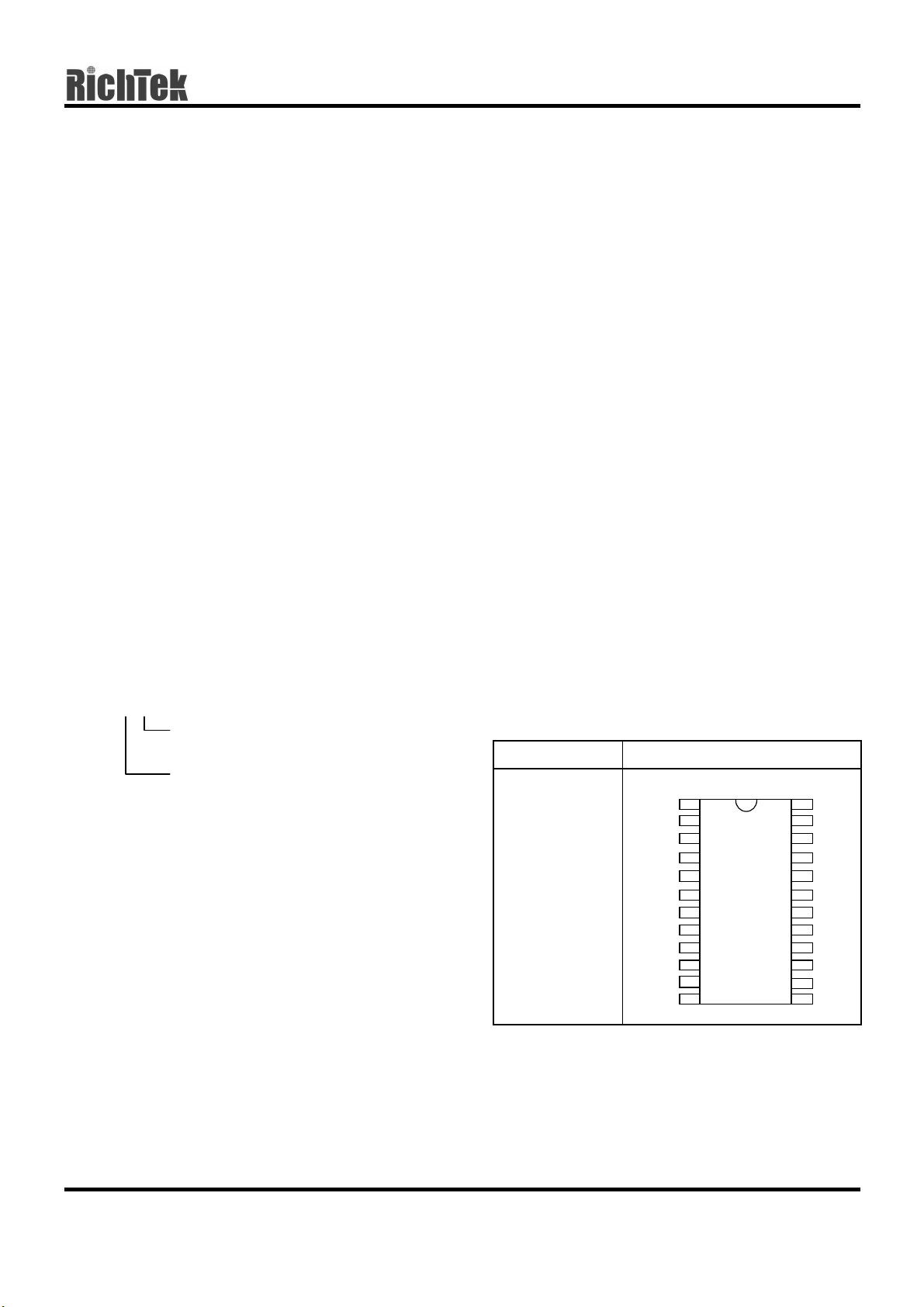
Pin Configurations
Part Number Pin Configurations
RT9221CS
(Plastic SOP-24)
GND
GATE1
LDOS1
LDOS2
VCC
OVP
PGOOD
CSN
CSP
PGNDH
DH BSTL
PGNDL
TOP VIEW
1
2
3
4
5
6
7
8
9
10
11
12 13
24
23
22
21
20
19
18
17
16
15
14
GATE2
LDOV
VID0
VID1
VID2
VID3
VID4
VSEN
SHDN
BSTH
DL
DS9222-05 May 2001 www.richtek-ic.com.tw
1
RT9221
Absolute Maximum Ratings
z VCC to GND -0.3 to +5.5V
z PGND to GND ± 0.3V
z BSTH and BSTL to GND -0.3 to +14V
z Ambient Temperature Range 0 to +70°C
z Junction Temperature Range 0 to +125°C
z Storage Temperature Range -65 to +150°C
z Lead Temperature (Soldering, 10 sec.) 300°C
z Package Thermal Resistance
SOP-24, θ
JA
Electrical Characteristics
75°C/W
(VCC = 5V; GND = 0V; PGNDH = PGNDL = 0V; VSEN = VOUT; 0mV < (V
CSP-VCSN
) < 60mV; T
= 25°C)
A
Parameter Symbol Test Conditions Min Typ Max Units
Switching Section
Output Voltage
Supply Voltage
Supply Current
Load Regulation
Line Regulation
V
OUT
V
CC
I
CC
∆V
LOADIO
∆V
LINE
IO = 2A
VCC 4.5 -- 5.5 V
= 0.8A to 15A
VCC = 4.75V to 5.25V -- 0.5 -- %
-- (1) -- --
-- 3 6 mA
-- 1 -- %
Power On Reset Trip Point VCC Rising -- 4.2 --
Current Limit Voltage
V
LIMIT
V
CSP
- V
CSN
65 75 85
Oscillator Frequency 170 200 230
Oscillator Max Duty Cycle
DH Source
DH Sink
DL Source
DL Sink
D
MAX
V
V
V
V
BSTH
- V
DH
BSTH
- V
DL
- V
DH
PGNDH
- V
DL
PGNDL
= 1V
= 1V
= 3V
= 1V
90 95 --
-- 3.5 --
-- 3.5 --
-- 2 --
-- 2 --
OVP Threshold Voltage 114 120 122
V
mV
KHz
%
Ω
Ω
Ω
Ω
%
OVP Source Current
I
OVP
V
OVP
= 3.0V
Power Good Threshold Voltage VSEN Rising 87 -- 113
10 -- --
mA
%
Linear Sections
Quiescent Current
I
Q
Output Voltage (LDO1 RT9221) 2.450 2.500 2.550
Output Voltage (LDO2 RT9221) 1.470 1.500 1.530
Gain (AOL)
Load Regulation
Line Regulation
∆V
LOADIO
∆V
LINE
LDOV = 12V ----5
LDOS (1,2) to GATE (1,2) -- 65 --
= 0 to 5A
-- 1 --
LDOV = 11.4V to 12.6V -- 1 --
mA
V
V
dB
%
%
Note: (1) See output voltage table.
www.richtek-ic.com.tw DS9222-05 May 2001
2
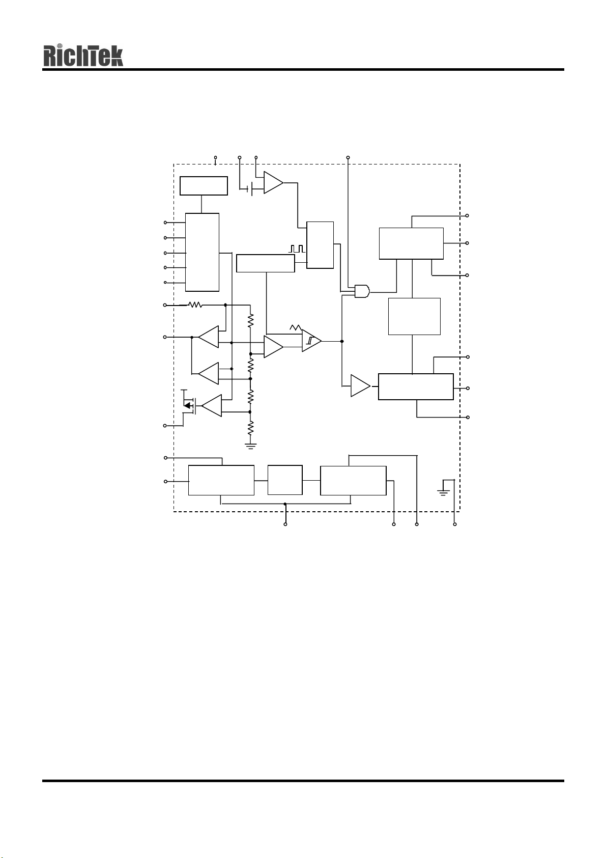
Function Block Diagram
1. 25 V REF
VID4
VID3
VID2
VID1
VID0
DAC
VCC
CSN
CSP
+
_
70mV
OSCILLATOR
CURRENT LIMI T
R
Q
S
SHDN
LEVEL SHIFT
AND DRI VER
RT9221
BSTH
DH
PGNDH
VSEN
PGOOD
OVP
LDOS 1
GATE1
OPEN
DRAIN
_
_
VCC
LINEAR
CONTROLLER
2. 5V
SHOOT-
200KHz
REF
_
+
CONTROLLER
LINEAR
1. 5V
+
+
+
_
+
_
ERRO R AM P
GND
1. 26 5V
LDOV
THROUGH
CONTROL
DRIVER
LDOS 2GATE2
BSTL
DL
PGNDL
GND
DS9222-05 May 2001 www.richtek-ic.com.tw
3

RT9221
Pin Description
Pin No. Pin Name Pin Function
1 GND Small signal analog and digital ground
2 GATE1 LDO1 gate drive output
3 LDOS1 LDO1 sense input
4 LDOS2 LDO2 sense input
5 VCC Input voltage
6OVP
7
PGOOD
High signal out if V
(1)
Open collector logic output; High if V0 within 10% of the setting point
> setting point + 20%
0
8 CSN Current sense input (Negative)
9 CSP Current sense input (Positive)
10 PGNDH High side drive GND
11 DH High side drive output
12 PGNDL Low side drive GND
13 DL Low side drive output
14 BSTL Supply for low side driver
15 BSTH Supply for high side driver
16
SHDN
(1)
Logic low shutdown the converter
17 VSEN Top end of internal feedback chain
18
19
20
21
22
VID4
VID3
VID2
VID1
VID0
(1)
(1)
(1)
(1)
(1)
Programming input (MSB)
Programming input
Programming input
Programming input
Programming input (LSB)
23 LDOV +12V for LDO section
24 GATE2 LDO2 gate drive output
Note: (1) All logic level inputs and outputs are TTL compatible.
www.richtek-ic.com.tw DS9222-05 May 2001
4
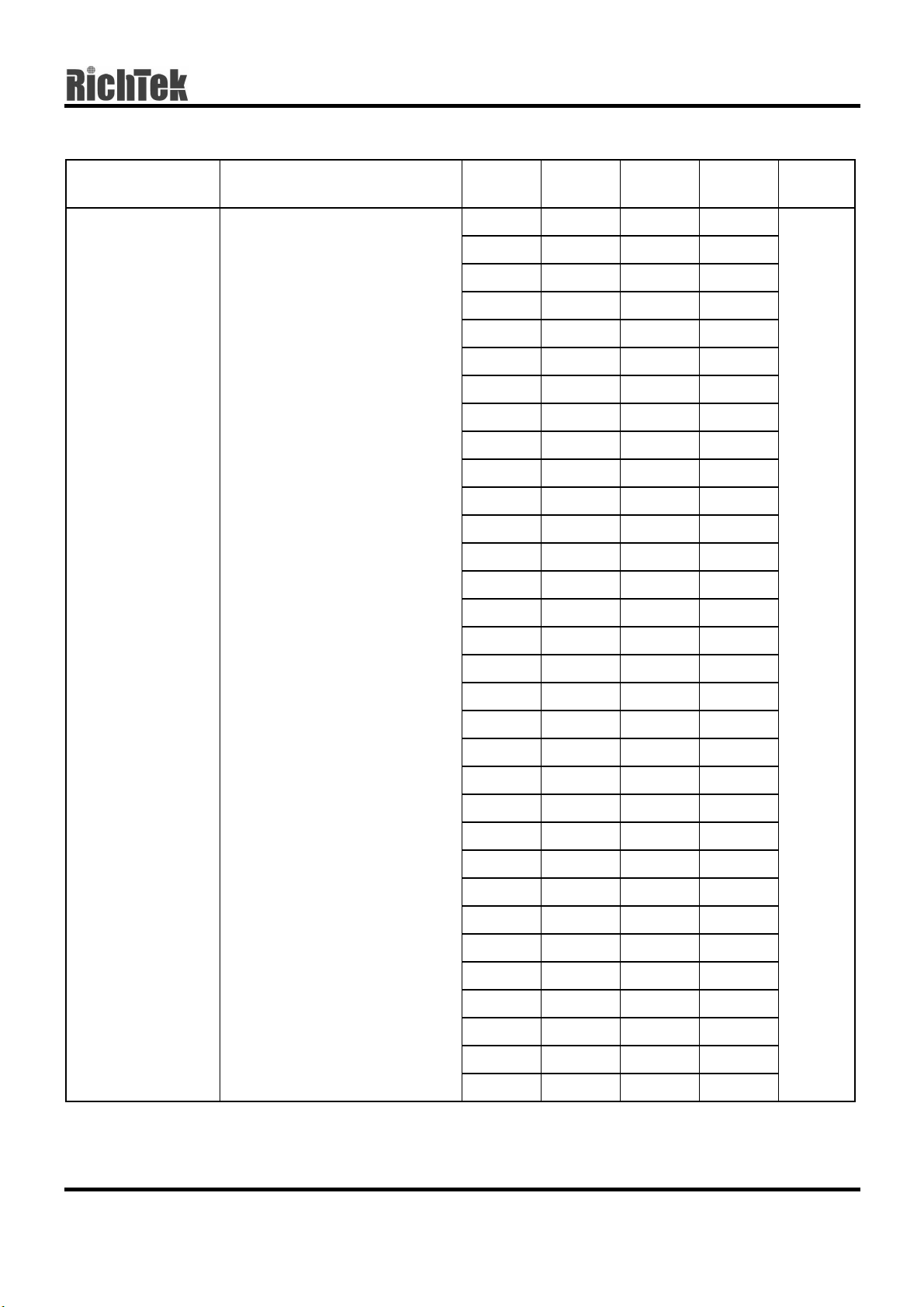
Table 1 Output Voltage Program
RT9221
Test Conditions
Output Voltage IO = 2A in application circuit
VID
43210
01111 1.287 1.300 1.313
01110 1.336 1.350 1.364
01101 1.386 1.400 1.414
01100 1.435 1.450 1.465
01011 1.485 1.500 1.515
01010 1.534 1.550 1.566
01001 1.584 1.600 1.616
01000 1.633 1.650 1.667
00111 1.683 1.700 1.717
00110 1.732 1.750 1.768
00101 1.782 1.800 1.818
00100 1.831 1.850 1.869
00011 1.881 1.900 1.919
00010 1.930 1.950 1.970
00001 1.980 2.000 2.020
Min Typ Max Units
V
00000 2.029 2.050 2.071
11111 1.980 2.000 2.020
11110 2.079 2.100 2.121
11101 2.178 2.200 2.222
11100 2.277 2.300 2.323
11011 2.376 2.400 2.424
11010 2.475 2.500 2.525
11001 2.574 2.600 2.626
11000 2.673 2.700 2.727
10111 2.772 2.800 2.828
10110 2.871 2.900 2.929
10101 2.970 3.000 3.030
10100 3.069 3.100 3.131
10011 3.168 3.200 3.232
10010 3.267 3.300 3.333
10001 3.366 3.400 3.434
10000 3.465 3.500 3.535
DS9222-05 May 2001 www.richtek-ic.com.tw
5

RT9221
Typical Application Circuit
12V
5V
+
C10
C2
0.1µF
R9
5
Ω
R1
10KR210
C4
5
6
OVP
22
VID0
21
VID1
20
VID2
19
VID3
16
SHDN
1
GND
PGNDL
24
GATE2
2
GATE1
43
LDOS2
RFD3055
VID0
VID1
VID2
VID3
VID4
OVP
SHDN
PGOOD
1000µF
5V
5V
C9
C1
0.1µF
1500µFx2
++
1000µF
R14
10
VCC
R13
10
RT9221
Q4
C14
1µF
CSP
CSN
VSEN
PGOOD
VID4
BSTH
DH
PGNDH
DL
BSTL
LDOV
LDOS1
C11
0.1µF
17
7
18
15
11
10
1312
14
23
C13
1µF
R3
10K
9
8
R8
5
Ω
+
0.1µF
PHB83N03LT
Q1
Q2
PHB95N03LT
C12
1000µF
C3
L1
4µH
R4
1.0K
R6
5m
RFD3055
Q3
C8
0.1µF
R5
2.32K
Ω
+
C5 C6
1500µFx4
0.1µF
+
C7
1000µF
VCC_ CORE
GND
VLIN1
VLIN2
www.richtek-ic.com.tw DS9222-05 May 2001
6

Package Information
RT9221
H
M
B
A
C
FD
Dimensions In Millimeters Dimensions In Inches
Symbol
Min Max Min Max
A 15.189 15.596 0.598 0.614
B 7.391 7.595 0.291 0.299
C 2.362 2.642 0.093 0.104
D 0.330 0.508 0.013 0.020
I
B
J
F 1.194 1.346 0.047 0.053
H 0.229 0.330 0.009 0.013
I 0.102 0.305 0.004 0.012
J 10.008 10.643 0.394 0.419
M 0.381 1.270
DS9222-05 May 2001 www.richtek-ic.com.tw
0.015 0.050
7

RT9221
RICHTEK TECHNOLOGY CORP.
Headquarter
6F, No. 35, Hsintai Road, Chupei City
Hsinchu, Taiwan, R.O.C.
Tel: (8863)5510047 Fax: (8863)5537749
www.richtek-ic.com.tw DS9222-05 May 2001
RICHTEK TECHNOLOGY CORP.
Taipei Office (Marketing)
8F-1, No. 137, Lane 235, Paochiao Road, Hsintien City
Taipei County, Taiwan, R.O.C.
Tel: (8862)89191466 Fax: (8862)89191465
Email: marketing@richtek-ic.com.tw
8
 Loading...