Preliminary
RT9182
Dual, Low-Noise, 200mA LDO Regulator
General Description
The RT9182 is a dual-channel, low noise, and low
dropout regulator supplying up to 200mA current at
each channel. The output voltage ranges from 1.5V
to 3.3V in 100mV increments and 2% accuracy by
operating from a +2.7V to +6.5V input.
The RT9182 uses an internal PMOS as the pass
device, which consumes 165µA supply current (both
LDOs on) independent of load current and dropout
conditions. The SHDN pin controls both outputs
simultaneously and consumes nearly zero operation
current in the disable mode making the IC suitable
for battery-power devices. Other features include a
reference voltage bypass pin to improve low noise
performance, current limiting, and over temperature
protection.
Ordering Information
RT9182
Package type
E : SOT-26
Operating temperature range
C : Commercial standard
Features
•
Up to 200mA Output Current (Each LDO)
•
Shutdown Function
•
29µµµµV
•
Current Limiting and Thermal Protection
•
Short Circuit Protection
•
120mV Dropout at 100mA Load
•
Two LDOs in SOT-26 Package
Low Noise Output
RMS
Applications
Cellular Phones
z
Laptop, Notebook, and Palmtop Computers
z
Battery-powered Equipment
z
Hand-held Equipment
z
Pin Configurations
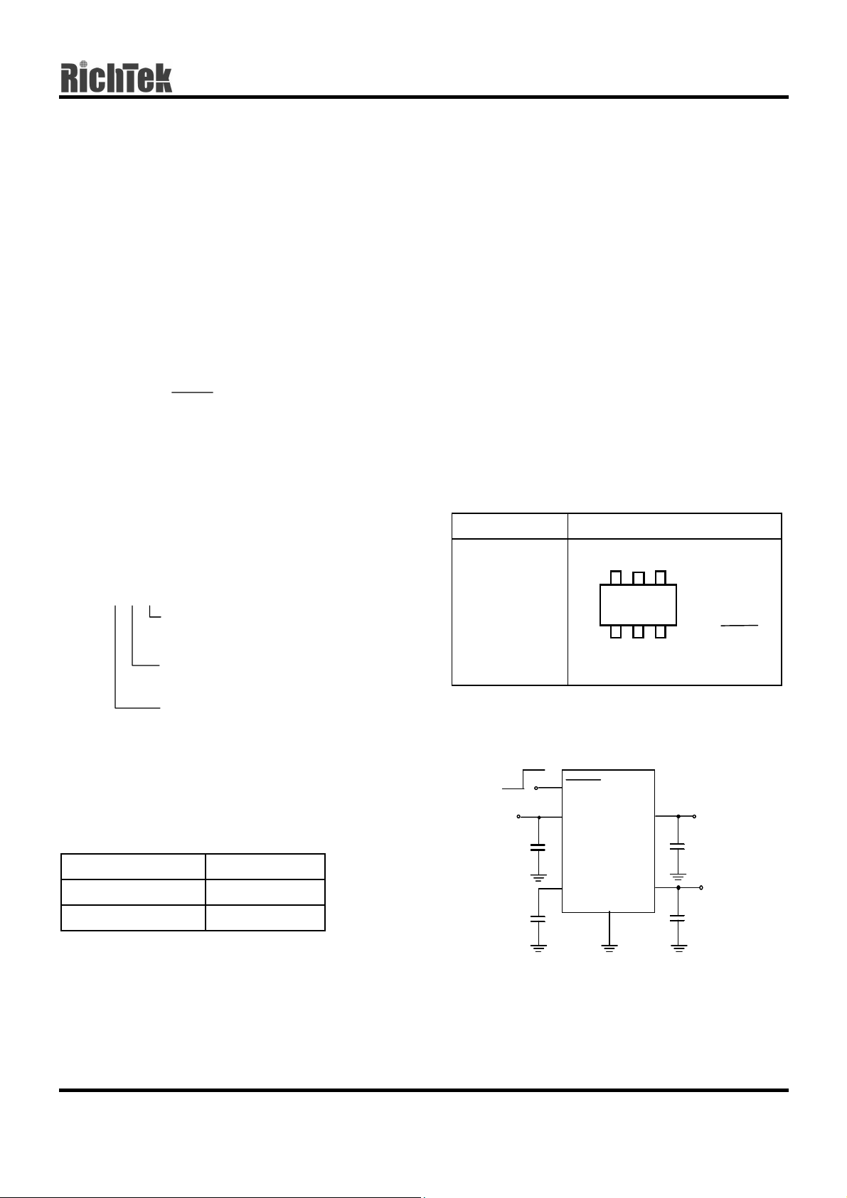
Part Number Pin Configurations
RT9182CE
64
(Plastic SOT-26)
5
321
TOP VIEW
1. VOUT2
2. GND
3. BP
4. SHDN
5. VIN
6. VOUT1
Output voltage
Typical Application Circuit
A : 2.8V (Output1), 2.8V (Output2)
B : 3.0V (Output1), 3.0V (Output2)
ON
Marking Information
V
OFF
OU T2
2. 2
F
µ
SHDN
RT9182
VOUT1VOUT2
V
2. 2µF
OU T1
Part Number Marking
2. 2µF
V
IN
RT9182ACE 2M
RT9182BCE 2Q
DS9182-02 April 2002 www.richtek-ic.com.tw
10nF
BP
VIN
GND
1

RT9182
Pin Description
Pin Name Pin Function
VOUT2 Output2 Voltage
GND Ground
BP Reference Noise Bypass
SHDN Active Low Shutdown Input
VIN Power Input
VOUT1 Output1 Voltage
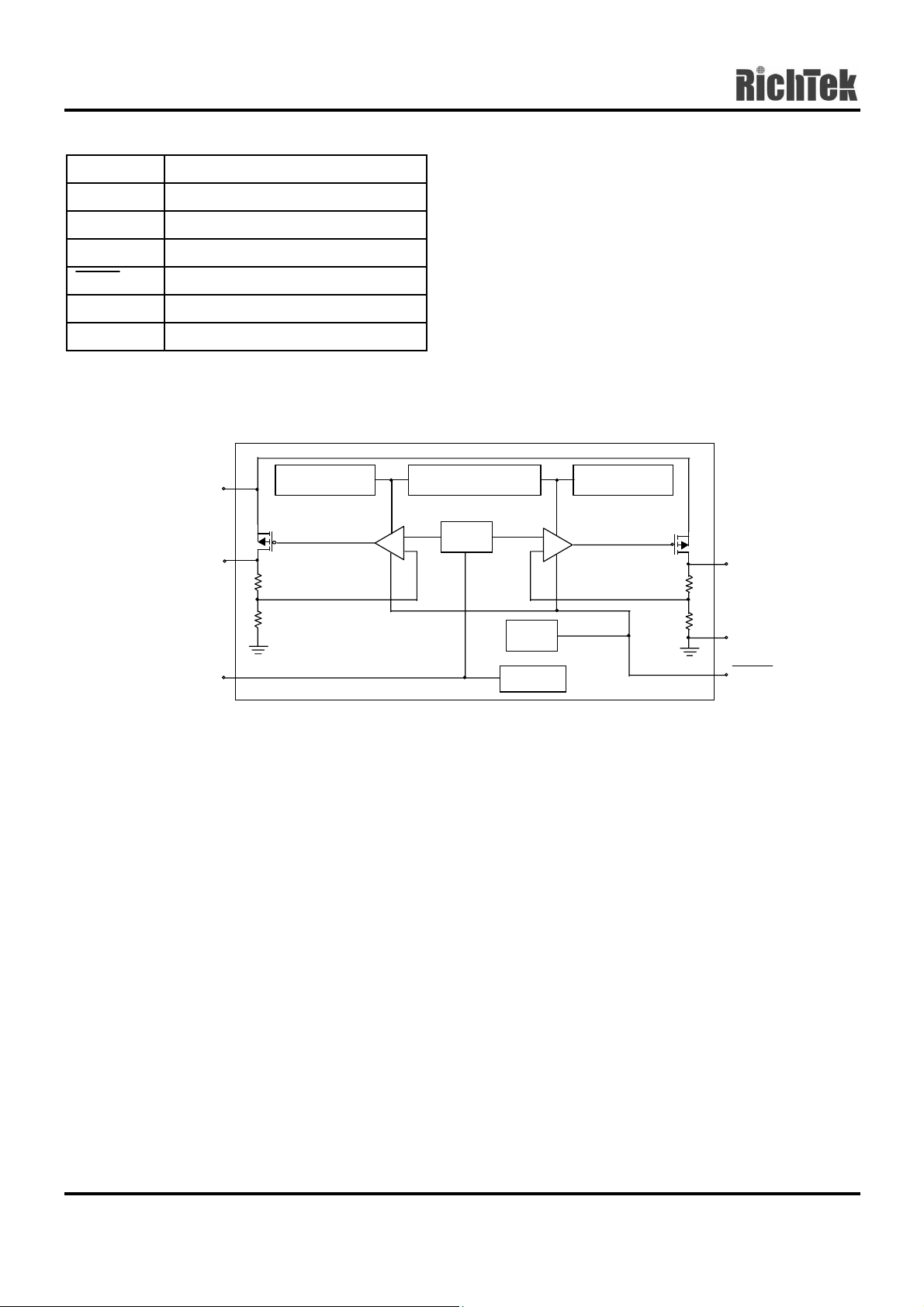
Function Block Diagram
Preliminary
VIN
VOUT1
BP
Thermal ProtectionCurrent Limit Current Limit
_
+
Vref
+
Bias
Start-Up
_
VOUT2
GND
SHDN
www.richtek-ic.com.tw DS9182-02 April 2002
2

Preliminary
RT9182
Absolute Maximum Ratings
z Input Voltage 7V
z Power Dissipation, P
@ TA = 25°C
D
SOT-26 748mW
z Junction Temperature Range -40°C ~ 125°C
z Storage Temperature Range -65°C ~ 150°C
z Operating Temperature Range -40°C ~ 85°C
z Lead Temperature (Soldering, 10 sec.) 260°C
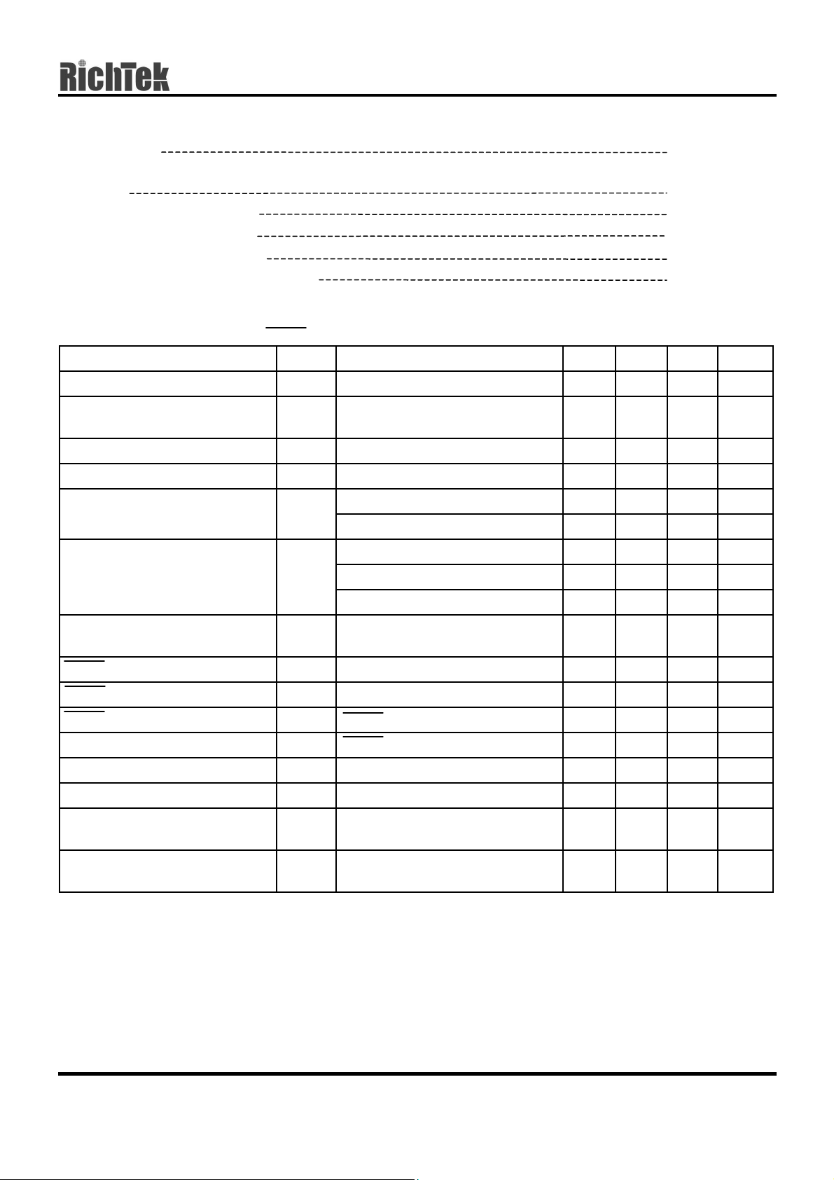
Electrical Characteristics
(V
= 3.6V, CIN = C
IN
Parameter Symbol Test Conditions Min Typ Max Units
= 2.2µF, SHDN = VIN, typical values at TA = 25°C, for each LDO unless otherwise specified.)
OUT
Input Voltage Range
Output Voltage Accuracy
(Load Regulation)
Maximum Output Current
Current Limit
V
IN
∆V
OUTIL
I
MAX
I
LIMIT
= 1mA to 200mA
Continuous 200 -- -- mA
R
= 1Ω
LOAD
2.7 -- 6.5 V
-2 -- +2 %
200 -- 550 mA
No Load -- 165 260
GND Pin Current
Dropout Voltage
(Note)
Line Regulation
SHDN Input High Threshold
SHDN Input Low Threshold
SHDN Input Bias Current
Shutdown Supply Current
I
G
V
DROP
∆V
V
IH
V
IL
I
SD
I
GSD
I
OUT
I
OUT
I
OUT
I
OUT
VIN = (V
LINE
I
OUT
VIN = 2.7V to 6.5V
VIN = 2.7V to 6.5V
SHDN = GND or V
= 100mA (Both LDOs)
= 1mA
= 100mA
= 200mA
+0.4V or 2.7V) to 6.5V
OUT
= 1mA
IN
-- 165 260
-- 1.2 -- mV
-- 120 -- mV
-- 255 -- mV
-0.2 -- +0.2 %/V
1.6 -- --
-- -- 0.4
-- -- 100
SHDN = GND -- 0.01 1
Thermal Shutdown Temperature -- 140 --
µA
µA
V
V
nA
µA
°C
Thermal Shutdown Hysteresis
Output Voltage Noise
Output Voltage AC PSRR
Note : Dropout voltage definition: VIN – V
DS9182-02 April 2002 www.richtek-ic.com.tw
T
SD
e
NO
10Hz to 100kHz, CBP = 10nF
C
= 4.7µF, I
OUT
OUT
100Hz, C
I
= 100mA
LOAD
when V
OUT
LOAD
= 10nF, C
BP
is 50mV below the value of V
= 1mA
OUT
= 4.7µF
-- 10 --
-- 29 --
-- 62 --
(normal)
OUT
µV
°C
RMS
dB
3
 Loading...