

Page 1
Preliminary
RT9181
150mA LDO Regulator with POG
General Description
The RT9181 is a low dropout voltage regulator with
an output 2% accuracy and supply a continuous
150mA current within operating range from a +3V to
+5.5V input. The power good function monitors the
output voltage and indicates by pulling low the power
good output (open drain).
The RT9181 requires a small output capacitor with
low ESR for stabilizing output voltage. The device
also minimizes output overshoot during power up.
The RT9181 uses an internal PMOS as the pass
device, which consumes 160µA supply current
independent of load and dropout conditions. The CE
pin controls the output and consumes no input bias
current. Other features include current limiting, over
temperature protection, and under voltage lockout.
Applications
Processor Power-Up Sequencing
z
Laptop, Notebook, and Palmtop Computers
z
Features
z
Low Dropout Voltage Regulator, Output 1.2V
z
Up to 150mA Output Current
z
Power Good (POG) Function
z
Chip Enable/Shutdown Function
z
Load Independent, Low Ground Current, 160µµµµA
z
Current Limiting and Thermal Protection
z
Under Voltage Lockout (UVLO)
z
Low Variation Due to Load and Line Regulation
z
Output Stable with Low ESR Capacitors
z
SOT-25 Package
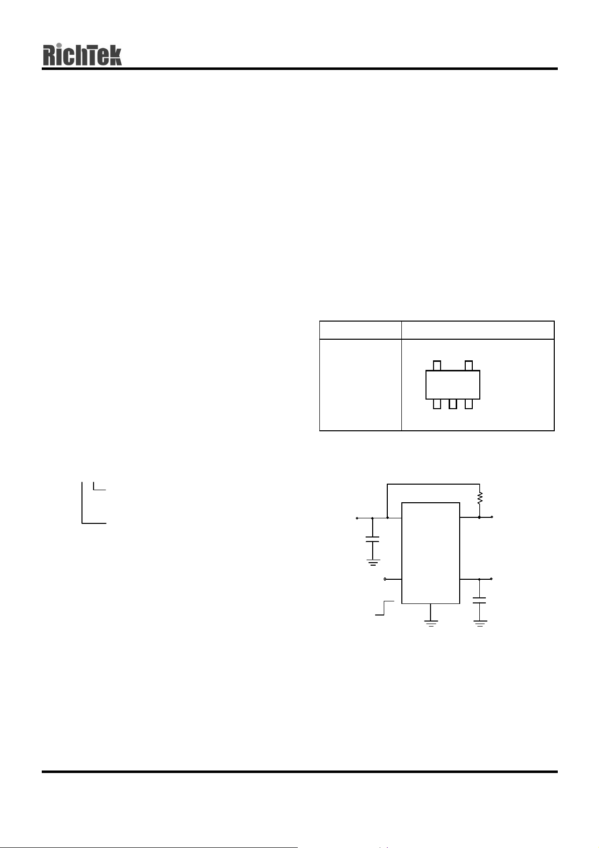
Pin Configurations
Part Number Pin Configurations
RT9181CB
(Plastic SOT-25)
54
3
21
TOP VIEW
1. VIN
2. GND
3. CE
4. POG
5. VOUT
Ordering Information
RT9181
Package type
B : SOT-25
Operating temperature range
C: Commercial standard
Typical Application Circuit
10K
C
IN
1µF
ON
VIN
CE
V
IN
OFF
POG
VOUT
GND
C
OU T
1µF
POG
V
OUT
DS9181-00 February 2002 www.richtek-ic.com.tw
1
Page 2
RT9181
Pin Description
Pin Name Pin Function
VIN Input Pin
GND Power Ground Pin
CE Enable/Shutdown Input (Active High)
POG Power Good Indicator
VOUT Output Pin
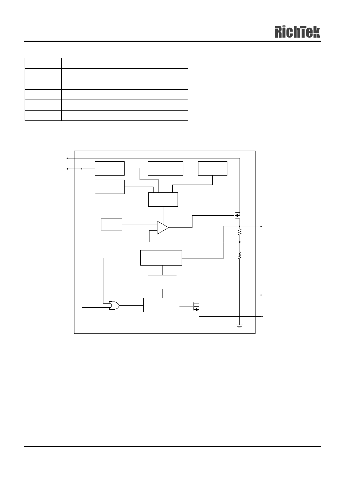
Function Block Diagram
VIN
CE
Shutdown
Control
Thermal
Sensor
Preliminary
Undervoltage
Loc kout
Gate
Control
Current
Limit
Verf
Fault
_
+
Output Voltage
Detection
GOOD
Delay
Timer
Power Good
Control
VOUT
POG
GND
www.richtek-ic.com.tw DS9181-00 February 2002
2
Page 3

Preliminary
(
))
y
)
g
RT9181
Absolute Maximum Ratings
z
Input Voltage, VIN 7V
z
CE Input Voltage 7V
z
Power Good Output Voltage 7V
z
Power Dissipation, PD @ TA = 25°C
SOT-25 570mW
z
Junction Temperature Range -40°C ~ 125°C
z
Storage Temperature Range -65°C ~ 150°C
z
Operating Temperature Range 0°C ~ 70°C
z
Lead Temperature (Soldering, 10 sec.) 260°C
Electrical Characteristics
(V
= 5V, CIN = C
IN
Parameter Symbol Test Conditions Min Typ Max Units
= 1µF, TA = 25°C, unless otherwise specified)
OUT
Input Voltage Range V
IN
3--5.5V
IL = 25mA 1.182 1.2 1.218
Output Voltage Accuracy ∆V
OUT
IL = 0.1mA, TA = 0°C to 70°C (Note) -2 -- +2
%
Output Load Current Continuous 150 -- -- mA
Current Limit I
GND Current I
LIMIT
G
Line Regulation ∆V
Load Regulation ∆V
Dropout Voltage V
DROPIL
R
= 1Ω 160 300 -- mA
LOAD
No Load 90 160 250 µA
LINEVIN
LOADIL
= 0.1mA to 150mA -- -- +3 %
= 3 to 5.5V, I
= 0.1mA -0.3 -- +0.3 %
OUT
= 150mA -- 1 -- V
CE Input High Threshold VIN = 3 to 5.5V 2 -- -- V
CE Input Low Threshold VIN = 3 to 5.5V -- -- 0.8 V
CE Input Bias Current CE = GND or V
IN
-- -- 100 nA
CE Supply Current CE = GND -- 0.01 -- µA
V
POGH
V
POGH
Power Good Low Threshold
Power Good High Threshold
Output falls % of V
timer
Power good
Output reaches % of V
dela
timer (power good
(power NOT
OUT
OUT
, start
85 -- -- %
-- -- 90 %
VOL Power Good Output Logic Low Fault condition, IOL = 100µA----0.4V
td
Power Up Overshoot
Thermal Shutdown Temperature T
Delay Time to Power Good See timing diagram 1 2 5 mS
(POG)
SD
Maximum voltage overshoot allowed
on output durin
power-up
-- 1 -- %
-- 150 -- °C
Thermal Shutdown Hysteresis -- 20 -- °C
Output Voltage AC PSRR 100Hz, C
OUT
= 1µF, R
= 100Ω -- 62 -- dB
LOAD
Note: Assured by design, not tested in production
DS9181-00 February 2002 www.richtek-ic.com.tw
3
Page 4

RT9181
Typical Operating Charateristics
Preliminary
Output Voltage vs. Temperature
1.210
1.205
1.200
Output Voltage (V)
1.195
1.190
-20 0 20 40 60 80
Temperature ( C)
°
Current Lim it vs. Temperature
400
350
V
IN
I
LOAD
= 5V
= 0.1mA
Output Voltage vs. Supply Voltage
1.210
1.205
1.200
Output Voltage (V)
1.195
1.190
3.0 3.5 4.0 4.5 5.0 5.5 6.0
Supply Volta ge (V)
Current Limit vs. Supply Voltage
400
350
I
LOAD
= 0.1mA
300
Current Limit (mA)
250
200
-20 0 20 40 60 80
Temperature ( C)
°
Quiescent Current vs. Temperature
180
175
µ
170
165
160
Quiescent Current ( A)
155
150
-20 0 20 40 60 80
Temperature ( C)
°
V
= 5V
IN
VIN = 5V
300
Current Limit (mA)
250
200
33.544.555.56
Supply Voltage (V)
Quiescent Current vs. Supply Voltage
180
175
µ
170
165
160
Quiescent Current ( A)
155
150
3.0 3.5 4.0 4.5 5.0 5.5 6.0
Supply Voltage (V)
www.richtek-ic.com.tw DS9181-00 February 2002
4
Page 5

Preliminary
>
>
>2 >
>
>
)
>
>
>2 >
>
>
)
>
>
>2 >
>
>
)
y
RT9181
POG Delay Time vs. Temperature
3.0
2.5
2.0
1.5
1.0
POG Delay Time (mS)
0.5
0.0
-20 0 20 40 60 80
Temperature ( C)
°
Under Voltage Lock Out
V
IN
1
1
1 >1
T
POG Delay Time vs. Supply Voltage
3.00
2.50
2.00
1.50
1.00
POG Delay Time (mS)
0.50
= 5V
V
IN
0.00
3.0 3.5 4.0 4.5 5.0 5.5 6.0
Supply Volta ge (V)
POG Response at Power Down
T
POG
1
1
1 >1
V
OUT
2
2 >2
1) Ch 1: 2 Volt 5 ms
Ch 2: 500 mVolt 5 ms
2
POG Response vs. VOUT
POG
1
1
1 >1
V
OUT
2
2 >2
1) Ch 1: 5 Volt 1 ms
Ch 2: 500 mVolt 1 ms
2
1.2V
V
T
C
= 1µF
OUT
OUT
2
2 >2
1) Ch 1: 5 Volt 25 us
Ch 2: 500 mVolt 25 us
2
Time
T
T
V
= 5V
IN
C
= 1µF
OUT
Time
2ms
dela
T
VIN = 5V
Time
DS9181-00 February 2002 www.richtek-ic.com.tw
5
Page 6

RT9181
Timing Diagram
Preliminary
VOUT
POG
90% max of V
V
POGH
(norm al)
OU T
td(POG) 2.0ms typ.
Application Guides
CE/Shutdown
The RT9181 is enabled by driving the CE input high,
and shutdown by pulling the input low. If this feature
is not to be used, the CE input should be tied to VIN
to keep the regulator enabled at all times (the CE
input must not be left floating).
Internal P-Channel Pass Transistor
The RT9181 features a P-channel MOSFET pass
transistors. It provides several advantages over
similar designs using PNP pass transistors, including
longer battery life. The P-channel MOSFET requires
no base drive, which reduces quiescent current
considerably. PNP-based regulators waste
considerable current in dropout when the pass
transistor saturates, They also use high base-drive
currents under large loads. The RT9181 does not
suffer from these problems and consume only 160µA
of quiescent current whether in dropout, light-load, or
heavy-load applications.
Power Good
The power good output is an open-drain output. It is
designed essentially to work as a power-on reset
generator once the regulated voltage was up or a
fault condition. The output of the power good drives
low when a fault condition occurs. The power good
output come back up once the output has reached
90% of its nominal value and a 2.0ms (typ.) delay
has passed. See Timing Diagram. The output voltage
level will be drooped at the fault conditions including
current limit, thermal shutdown, or shutdown and
triggers the POG detector to alarm a fault condition.
This output is fed into an on-board delay circuitry that
V
POGL
85% min
drives the open drain transistor to indicate a fault.
Because at shutdown mode, a fault condition occurs
by pulling the POG output low, it will sink a current
from the open drain and the external power.
Selecting a suitable pulling resistance will be well to
control this dissipated power.
Current Limit and Thermal Protection
The RT9181 includes a current limit structure which
monitor and control the pass transistor’s gate voltage
limiting the guaranteed maximum output current to
150mA minimum.
Thermal-overload protection limits total power
dissipation in the RT9181. When the junction
temperature exceeds T
= +150°C, the thermal
J
sensor signals the shutdown logic turning off the
pass transistor and allowing the IC to cool. The
thermal sensor will turn the pass transistor on again
after the IC’s junction temperature cools by 20°C,
resulting in a pulsed output during continuous
thermal-overload conditions. Thermal-overloaded
protection is designed to protect the RT9181 in the
event of fault conditions. Do not exceed the absolute
maximum junction-temperature rating of T
= +125°C
J
for continuous operation. The output can be shorted
to ground for and indefinite amount of time without
damaging the part by cooperation of current limit and
thermal protection.
Operating Region and Power Dissipation
The maximum power dissipation of RT9181 depends
on the thermal resistance of the case and circuit
board, the temperature difference between the die
junction and ambient air, and the rate of air flow. The
www.richtek-ic.com.tw DS9181-00 February 2002
6
Page 7

Preliminary
RT9181
power dissipation across the device is
P = I
(VIN – V
OUT
OUT
)
The GND pin of the RT9181 performs the dual
function of providing an electrical connection to
ground and channeling heat away, Connect the GND
pin to ground using a large pad or ground plane.
Capacitor Selection and Regulator Stability
Like any low-dropout regulator, the external
capacitors used with the RT9181 must be carefully
selected for regulator stability and performance.
Using a capacitor whose value is ≥ 1µF on the
RT9181 input and the amount of capacitance can be
increased without limit. The input capacitor must be
located a distance of not more than 0.5” from the
input pin of the IC and returned to a clean analog
ground. Any good quality ceramic or tantalum can be
used for this capacitor. The capacitor with larger
value and lower ESR (equivalent series resistance)
provides better PSRR and line-transient response.
The output capacitor must meet both requirements
for minimum amount of capacitance and ESR in all
LDO applications. The RT9181 is designed
specifically to work with low ESR ceramic output
capacitor in space-saving and performance
consideration. Using a ceramic capacitor whose
value is at least 1µF with ESR is > 5mΩ on the
RT9181 output ensures stability. The RT9181 still
works well with output capacitor of other types due to
the wide stable ESR range. Output capacitor of larger
capacitance can reduce noise and improve load-
transient response, stability, and PSRR. The output
capacitor should be located not more than 0.5” from
the VOUT pin of the RT9181 and returned to a clean
analog ground.
large capacitor). If a tantalum capacitor is used at the
input, it must be guaranteed to have a surge current
rating sufficient for the application by the
manufacture.
Load-Transient Considerations
The RT9181 load-transient response graphs show
two components of the output response: a DC shift
from the output impedance due to the load current
change, and the transient response. The DC shift is
quite small due to the excellent load regulation of the
IC. Typical output voltage transient spike for a step
change in the load current from 0mA to 50mA is tens
mV, depending on the ESR and ESL of the output
capacitor. Increasing the output capacitor’s value and
decreasing the ESR and ESL attenuates the
overshoot.
Reverse Current Path
The power transistor used in the RT9181 has an
inherent diode connected between each regulator
input and output (see Fig.1). If the output is forced
above the input by more than a diode-drop, this diode
will become forward biased and current will flow from
the VOUT terminal to VIN. This diode will also be
turned on by abruptly stepping the input voltage to a
value below the output voltage. To prevent regulator
mis-operation, a Schottky diode could be used in the
applications where input/output voltage conditions
can cause the internal diode to be turned on (see
Fig.2). As shown, the Schottky diode is connected in
parallel with the internal parasitic diode and prevents
it from being turned on by limiting the voltage drop
across it to about 0.3V < 100mA to prevent damage
to the part.
Note that some ceramic dielectrics exhibit large
capacitance and ESR variation with temperature. It
may be necessary to use 2.2µF or more to ensure
Fig. 1
stability at temperatures below -10°C in this case.
Also, tantalum capacitors, 2.2µ or more may be
needed to maintain capacitance and ESR in the
stable region for strict application environment.
V
IN
V
OUT
Tantalum capacitors maybe suffer failure due to
surge current when it is connected to a low-
impedance source of power (like a battery or very
DS9181-00 February 2002 www.richtek-ic.com.tw
Fig. 2
7
Page 8

RT9181
Package Information
D
Preliminary
C
A
B
b
e
A1
Symbol
A 0.889 1.295 0.035 0.051
A1 0.000 0.152 0.000 0.006
Dimensions In Millimeters Dimensions In Inches
Min Max Min Max
H
L
B 1.397 1.803 0.055 0.071
b 0.356 0.559 0.014 0.022
C 2.591 2.997 0.102 0.118
D 2.692 3.099 0.106 0.122
e 0.838 1.041 0.033 0.041
H 0.102 0.254 0.004 0.010
L 0.356 0.610 0.014 0.024
SOT- 25 Surface Mount Package
www.richtek-ic.com.tw DS9181-00 February 2002
8
Page 9

Preliminary
RT9181
DS9181-00 February 2002 www.richtek-ic.com.tw
9
Page 10

RT9181
Preliminary
RICHTEK TECHNOLOGY CORP.
Headquarter
6F, No. 35, Hsintai Road, Chupei City
Hsinchu, Taiwan, R.O.C.
Tel: (8863)5510047 Fax: (8863)5537749
www.richtek-ic.com.tw DS9181-00 February 2002
RICHTEK TECHNOLOGY CORP.
Taipei Office (Marketing)
8F-1, No. 137, Lane 235, Paochiao Road, Hsintien City
Taipei County, Taiwan, R.O.C.
Tel: (8862)89191466 Fax: (8862)89191465
Email: marketing@richtek-ic.com.tw
10
 Loading...