

Page 1

Preliminary
RT9174
Triple Linear Regulator Controllers
General Description
The RT9174 is a triple linear regulator controller
designed for motherboard application.
The regulators are intended to regulate the
computer system AGP (2X/4X) power, the 2.5V
clock power, and the 1.8V power for North/South
Bridge core voltage and/or cache memory circuits.
All controllers can drive NPN or NMOSFET pass
transistor. A special scheme empoly driver voltage
could be higher than V
when driving NMOSFET
DD
through the 12V power.
The RT9174 future a small SOP-8 package for
saving board area. It also builds in current limiting
and thermal shutdown protection function.
Ordering Information
RT9174C S
Package type
S : SOP-8
Operating temperature range
C: Commercial standard
Features
z
Integrated Three Linear Controllers in a SOP-8
Package
z
Driving NPN or NMOSFET
z
Sourcing ( > 100mA) and Sinking ( > 5mA) Driver
z
Tri-State Output Driver
z
Low Internal 0.8V Reference
z
Adjustable Output Voltage Setting
z
High Output Stability
z
V
1.5/3.3V Automatic Changing for AGP
DDQ
z
Wide 3V ~ 8V Input Voltage Range
z
Current Limiting and Thermal Protection
Applications
Mother Boards Power Supply
z
Graphic Cards
z
Pin Configurations
Part Number Pin Configurations
RT9174CS
(Plastic SOP-8)
VDD
DRI 1
TOP VIEW
1
2
DRI 3
8
FB3
7
Function Block Diagram
VDD
DRI1
FB1
GND
Thermal
Limit
OC
+
_
_
+
0.8V 1.3 V
Referenc e
DRI 2
3
FB1
4
GND
OC
+
_
_
+
OC
+
_
_
+
DRI2
FB2
DRI3
FB3
6
FB2
5
DS9174-00 April 2001 www.richtek-ic.com.tw
1
Page 2
RT9174
Preliminary
Pin Description
Pin Name Pin Function
VDD Power Supply Input
DRI1 Regulator 1 Driver Output
FB1 Regulator 1 Feedback Non-inverting Input
GND Ground
DRI2 Regulator 2 Driver Output
FB2 Regulator 2 Feedback Non-inverting Input
DRI3 Regulator 3 Driver Output
FB3 Regulator 3 Feedback Non-inverting Input
Typical Application Circuit
C
1
1µF
1
VDD
2
DRI1
3
FB1
4
GND
RT9174
1
8
V
DDQ
1.5/ 3.3V
1000µF
12V
3.3V
PHD4 5N03 LT
C
+
2
0.1µF
Q
1
C
5
R
4.3K
R
4.99K
R
1
5K
2
3
C6
10nF
D
1N4148
R
1K
#TYPEDET3.3V
5V
DRI3
FB3
DRI2
FB2
3.3V
8
7
6
5
Q
2
2SD1802
R
4
250
+
R
5
200
V
O2
1.8V
C
3
470µF
Q
3
2SD1802
R
6
424
R
7
200
V
O3
2.5V
+
C
4
470µF
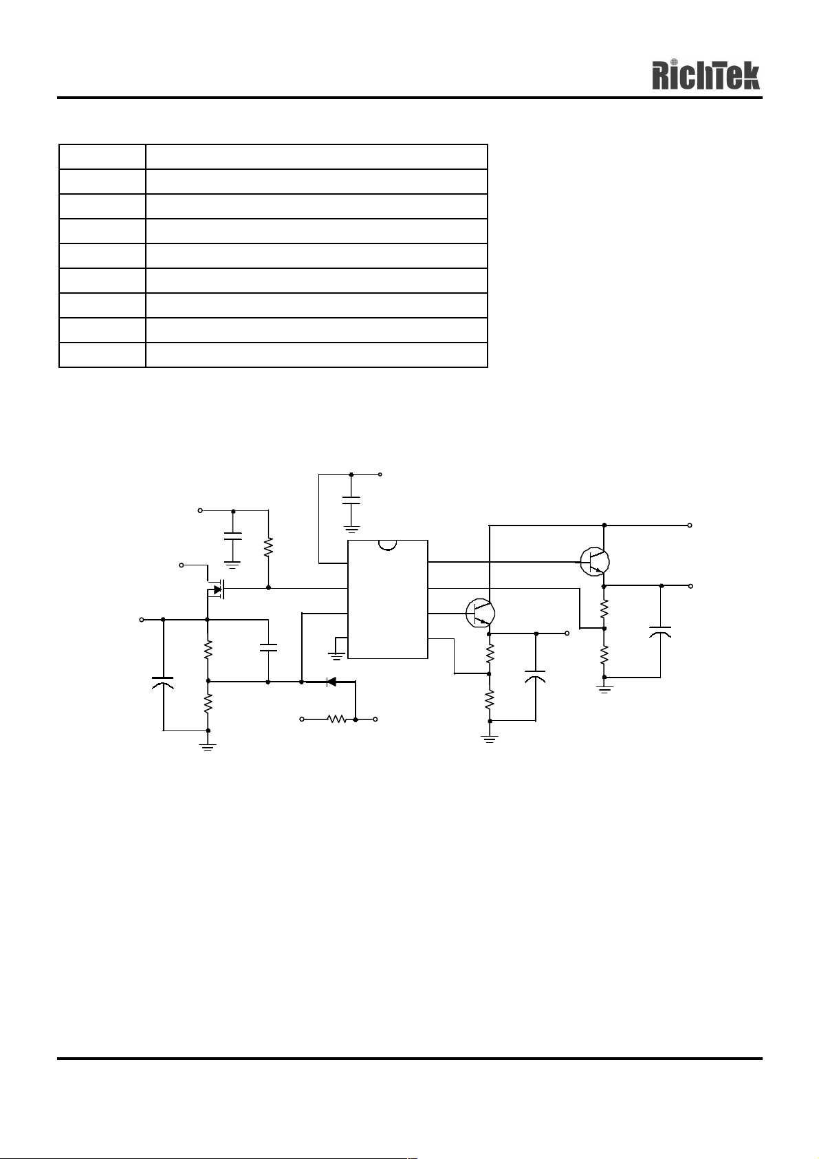
VDDQ = 3.3V if FB1 >1.3V
#TYPEDET = 0V →VDDQ = 1.5V
#TYPEDET = Open →VDDQ = 3.3V
Fig 1. Triple LDOs with VDDQ fo r M/B Application
www.richtek-ic.com.tw DS9174-00 April 2001
2
Page 3
12V
C
5
0.1µF
3.3V
Q
PHD4 5N03LT
V
DDQ
1.5/ 3.3V
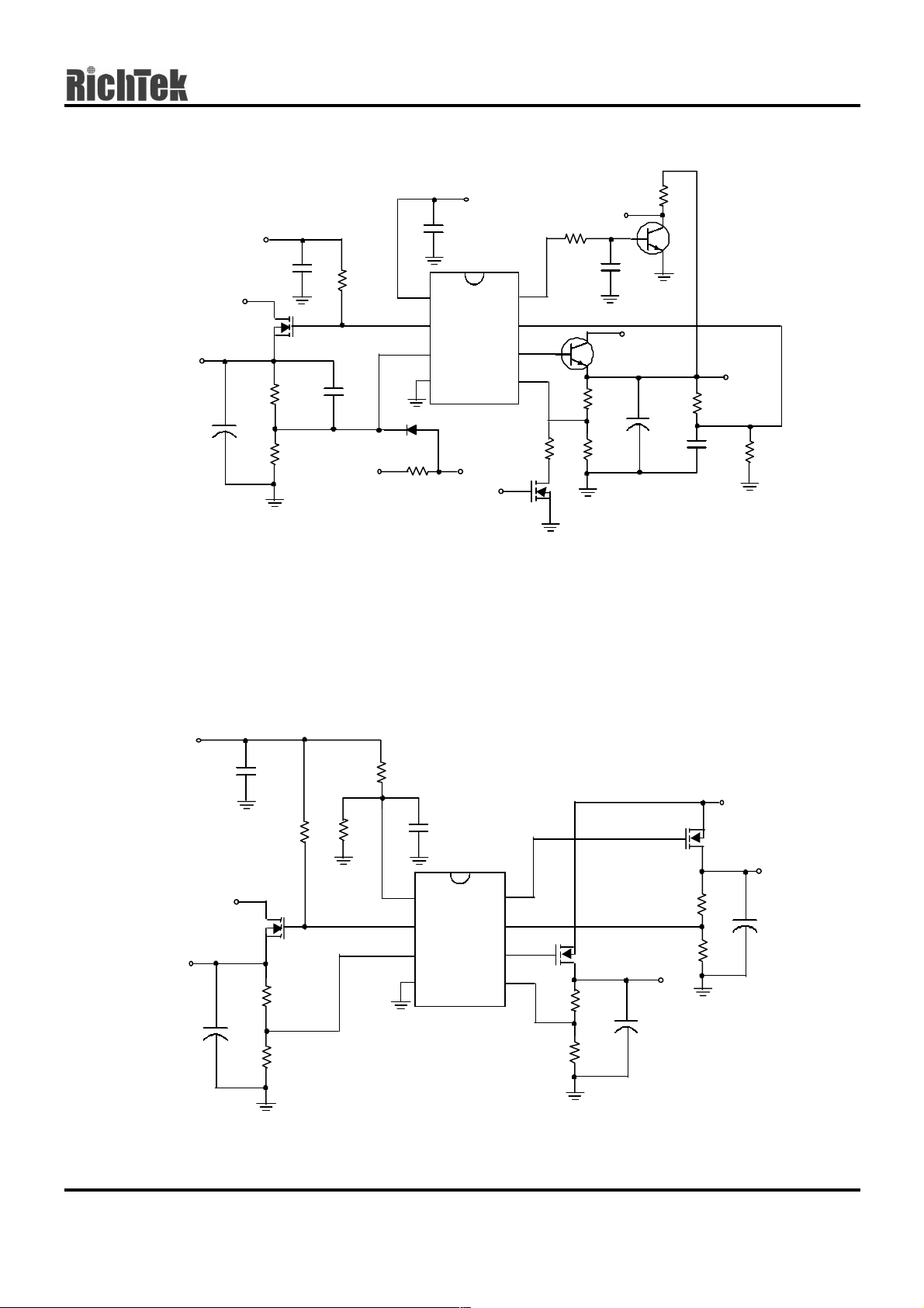
VDDQ = 3.3V if FB1 > 1.3V
#TYPEDET = 0V →VDDQ = 1.5V
#TYPEDET = Open →VDDQ = 3.3V
VTTSEL = 0V →VTT = 1. 2 5V
VTTSEL = 5V →VTT = 1. 5 V
1
R
2
+
4.3K
R
3
4.99K
R
1
5K
C6
10nF
Preliminary
C
1
1µF
1
VDD
2
DRI1
3
FB1
4
GND
RT91 74
D
1
1N4148
R
8
1K
#TYPEDET3.3V
5V
DRI3
FB3
DRI2
FB2
V
TTSEL
RT9174
R
V
TTPG
R
10
1K
C
8
7
6
5
R
11
374
Q
4
2N7002
8
0.01µF
3.3V
Q
2
2SD1802
R
4
113
+
R
5
200
1K
C
3
470µF
9
Q
MMBT39 04
R
3K
C
1µF
3
V
TT
6
7
R
12
8.2K
12V
PHD4 5N 03L T
V
O1
3.3V
C
2
1000µF
Fig 2. Dual LDOs with V
R
3K
R
9
1.2K
7.5V
C
8
1
1µF
1
VDD
2
DRI1
3
FB1
4
GND
DRI3
FB3
DRI2
FB2
RT9174
C
5
0.1µF
R
1
5K
5V
Q
1
R
2
+
624
R
200
3
for VRM8.5 Application
TTPG
8
7
6
5
Q
2
PHD4 5N 03L T
R
250
R
200
3.3V
Q
3
PHD4 5N 03L T
V
O3
R
424
R
O2
200
V
4
5
1.8V
+
C
3
470µF
2.5V
6
+
C
4
470µF
7
Fig 3. T ripl e LD Os Driving MOS Applicat ion
DS9174-00 April 2001 www.richtek-ic.com.tw
3
Page 4
RT9174
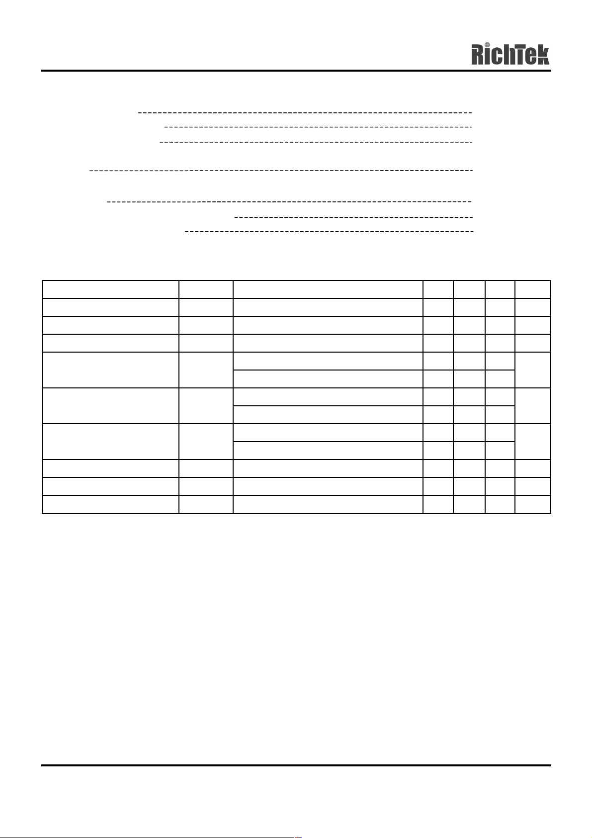
Absolute Maximum Ratings
Preliminary
z Input Voltage V
z Feedback FB1/FB2/FB3 -0.3 ~ 8V
z Driver DRI1/DRI2/DRI3 -0.3 ~ 12V
z Power Dissipation, P
DD
@ TA = 25°C
D
8V
SOP-8 0.625W
z Package Thermal Resistance
SOP-8, θ
z Operating Junction Temperature Range -40°C ~ 125°C
z Storage Temperature Range 65°C ~ 150°C
JA
160°C/W
Electrical Characteristics
(VDD = 5V, CIN = 1µF, TA = 25°C, unless otherwise specified)
Parameter Symbol Test Conditions Min Typ Max Units
Supply Current
Feedback Reference Voltage
Line Regulation
Load Regulation
Driving Capability
I
DD
V
∆V
∆V
I
O
REF
LINE
LOAD
No Load
No Load
VDD = 4V~7V
Source 100mA, DRI1/DRI2/DRI3 = 2.5V
Sink 5mA, DRI1/DRI2/DRI3 = 2.5V
Sourcing, DRI1/DRI2/DRI3 = 2.5V
Sink DRI1/DRI2/DRI3 = 2.5V
0.8 2 mA
0.78 0.8 0.82 V
210mV
510
mV
10
15
100
mA
5
Driver Current Limiting
Driver Tri-State Threshold
I
CL
V
TS
Thermal Limit
Power On Reset Voltage POR
Sourcing, DRI1/DRI2/DRI3 = 2.5V
Sink DRI1/DRI2/DRI3 = 2.5V
Sweep FB1/FB2/FB3 to Driver Output Off
300 700
mA
40 150
1.0 1.35 2.0 V
150
°C
2.4 V
www.richtek-ic.com.tw DS9174-00 April 2001
4
Page 5
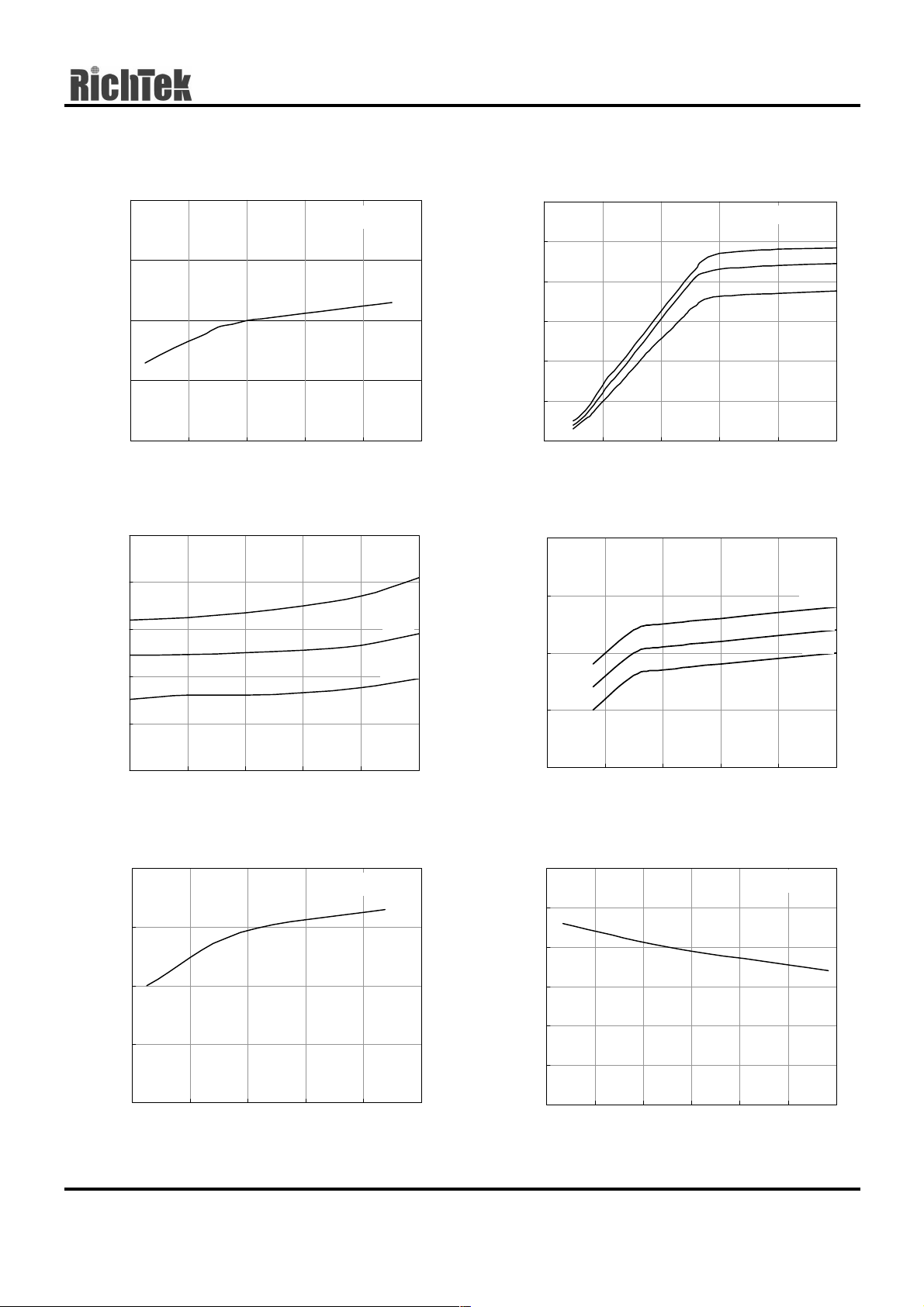
Typical Operating Charateristics
Preliminary
RT9174
0.82
0.81
0.80
Reference (Volt)
0.79
0.78
-50 -10 30 70 110 150
Temperature ( C)
°
Supply Current vs Temperature
1.4
1.2
1
IQ(mA)
0.8
0.6
Reference vs Tempature
300
V
= 5V
DD
250
200
150
Sourcing(mA)
100
50
0
012345
VDD - V
DRI1,2,3
(Volt)
Driver Sinking vs V
50
85°C
40
25°C
30
-20°C
Sinking (mA)
20
OUT
V
= 5V
DD
-20°C
25°C
85°C
V
= 5V
DD
-20°C
25°C
85°C
Driver Sourcing vs Drop Out
0.4
345678
VDD (Volt)
Tri-Sate Vth vs Temperature
1.6
V
= 5V
DD
1.4
1.2
10
012345
V
(Volt)
OUT
Short Current vs Tem perature
400
350
300
250
V
= 5V
DD
Vth(Volt)
200
1.0
0.8
-50 -10 30 70 110 150
Temperature( C)
°
Short Current (mA)
150
100
-50 -20 10 40 70 100 130
Temperature ( C)
°
DS9174-00 April 2001 www.richtek-ic.com.tw
5
Page 6
RT9174
Applications Information
Preliminary
Capacitors Selection
A 0.1µF minimum capacitor is recommended
between V
and ground to increase stability. The
DD
linear controllers use dominant pole compensation
integrated into the error amplifier and are sensitive to
output capacitor selection. When driving external
pass transistor, normally a minimum 470µF capacitor
must be placed at output for stability and good
transient response. When using internal pass
transistor, just need 10µF capacitor for stable.
Pass Transistor Selection
The RT9174 are designed specifically to driver
external NPN or NMOSFET pass transistor for up to
5A output current. The driver could deliver more
100mA when driving NPN transistor and sinking for a
pull up resistor load when driving a NMOSFET.
Typically pass transistor with NPN hfe > 50 at Imax or
NMOSFET Rds-on 100mΩ are suitable in most
application.
Layout Considerations
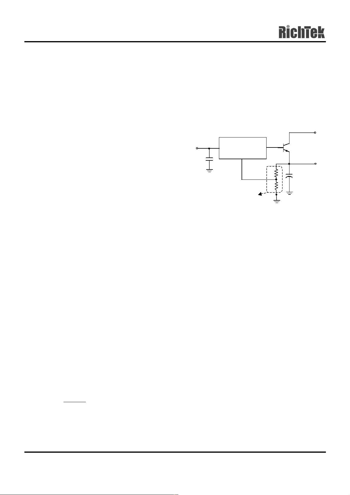
There are two critical layout considerations. One is
the divider resistors should be located to RT9174 as
possible to avoid inducing any noise. The second is
C
should be put at near the pass transistor to
OUT
avoid oscillation.
V
DRI1
V
DD
1µF
As close as to RT9174
VDD
RT9174
FB1
FB2
FB3
DRI2
DRI3
Fig 4
R1
R2
V
+
C
OUT
IN
OUT
Output Voltage Setting
The RT9174 develop a 0.8V reference voltage,
especially suit for low voltage application. As shown
in Fig. 4, the output voltage could be easy set by R1
& R2 resistor. The divided resistor must keep below
1KΩ for quick response and stability.
Tri-state Operation
A special Tri-state design is empolyed in the RT9174
for AGP 2X/4X power supply. Typical application
shown the detail circuit. In AGP 2X SELECT = open,
FB1 will be pulled up over 1.3V through R
Tri-state threshold. R
has to meet the following
8
to trip the
8
relationship:
R
< 0.75 (V33 - 1.3) ×R2,
8
+
RR
if
When in AGP 4X SELECT = GND, V
23
3
R
=×
1.50.8
.
will work in
DDQ
normal 1.5V setting.
www.richtek-ic.com.tw DS9174-00 April 2001
6
Page 7
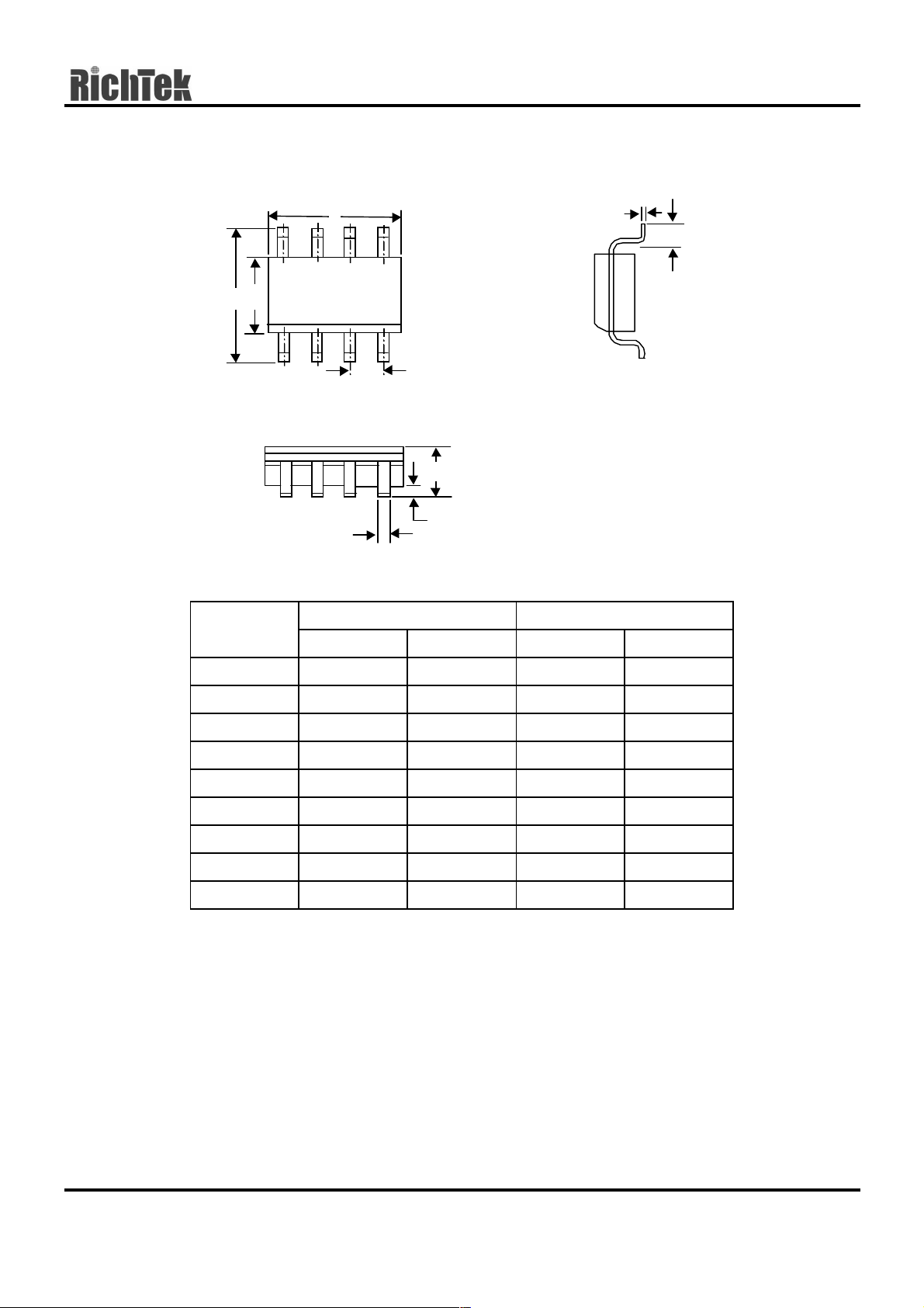
Package Information
B
J
A
Preliminary
H
M
F
C
RT9174
D
Dimensions In Millimeters Dimensions In Inches
Symbol
Min Max Min Max
A 4.801 5.004 0.189 0.197
B 3.810 3.988 0.150 0.157
C 1.346 1.753 0.053 0.069
D 0.330 0.508 0.013 0.020
F 1.194 1.346 0.047 0.053
H 0.178 0.254 0.007 0.010
I 0.102 0.254 0.004 0.010
J 5.791 6.198 0.228 0.244
M 0.406 1.270 0.016 0.050
8-Lead SOP Plastic Package
I
DS9174-00 April 2001 www.richtek-ic.com.tw
7
Page 8

RT9174
Preliminary
RICHTEK TECHNOLOGY CORP.
Headquarter
6F, No. 35, Hsintai Road, Chupei City
Hsinchu, Taiwan, R.O.C.
Tel: (8863)5510047 Fax: (8863)5537749
www.richtek-ic.com.tw DS9174-00 April 2001
RICHTEK TECHNOLOGY CORP.
Taipei Office (Marketing)
8F-1, No. 137, Lane 235, Paochiao Road, Hsintien City
Taipei County, Taiwan, R.O.C.
Tel: (8862)89191466 Fax: (8862)89191465
Email: [email protected]
8
 Loading...