Richtek RT9179GB, RT9179PB Schematic [ru]

Adjustable, 300mA LDO Regulator with Enable
RT9179
General Description
The RT9179 is a high performance linear voltage regulator
with enable high function and adjustable output with a
1.175V reference voltage. It operates from an input of 3V
to 5.5V and provides output current up to 300mA with two
external resistors to set the output voltage ranges from
1.175V to 4.5V.
The RT9179 has superior regulation over variations in line
and load. Also it provides fast respond to step changes in
load. Other features include over-current and over-
temperature protection. The device has enable pin to reduce
power consumption in shutdown mode.
The devices is available in the popular SOT-23-5 package.
Ordering Information
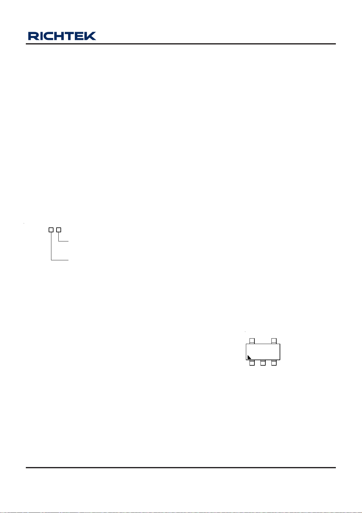
RT9179
Package Type
B : SOT-23-5
Lead Plating System
P : Pb Free
G : Green (Halogen Free and Pb Free)
Note :
Richtek products are :
` RoHS compliant and compatible with the current require-
ments of IPC/JEDEC J-STD-020.
` Suitable for use in SnPb or Pb-free soldering processes.
Features
zz
300mV Dropout @ 300mA
z
zz
zz
z 150uA Low Ground Pin Current
zz
zz
z Excellent Line and Load Regulation
zz
zz
z <1uA Standby Current in Shutdown Mode
zz
zz
z Guaranteed 300mA Output Current
zz
zz
z Stable with 1uF Input a nd Output Cera mic Ca pacitor
zz
zz
z Adjustable Output V oltage Ra nges from 1.175V to
zz
4.5V
zz
z Over-T emperature/Over-Current Protection
zz
zz
z RoHS Compliant and 100% Lead (Pb)-Free
zz
Applications
z Battery-Powered Equipment
z Graphic Card
z Peripheral Cards
z PCMCIA Card
Marking Information
For marking information, contact our sales representative
directly or through a Richtek distributor located in your
area.
Pin Configurations
(TOP VIEW)
VOUT
5
VIN
ADJ
23
EN
GND
4
SOT-23-5
DS9179-11 April 2011 www.richtek.com
1

RT9179
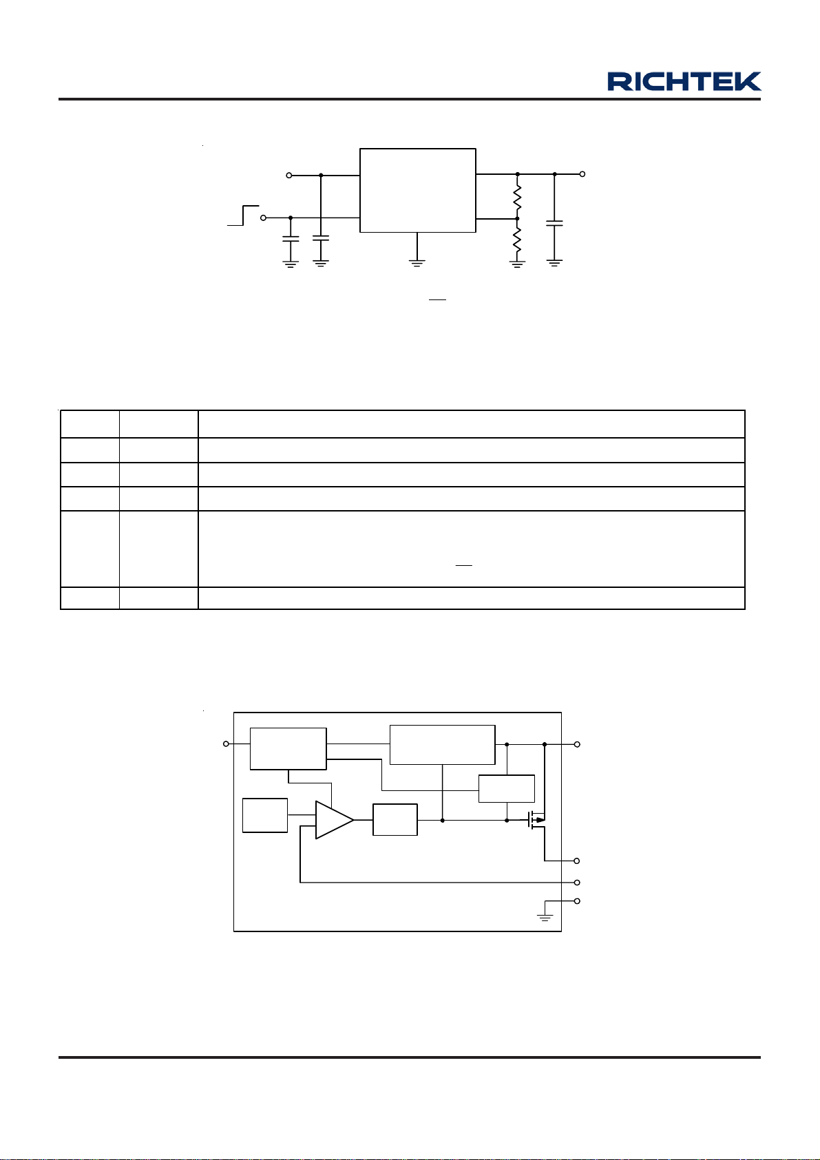
Typical Application Circuit
V
IN
Chip Enable
C
C
3
0.1uF
Note: The external feedback resistors are in hundreds of OHM to hundreds of kOHM ranges.
1
1uF
V
= 1.175 x ( ) Volts
OUT
RT9179
ADJ
GND
R
1+
R
VOUT
1
2
VIN
EN
Adjustable Operation
Functional Pin Description
Pin No. Pin Name Pin Function
1 VIN Power Input Voltage
2 GND Ground
3 EN Chip Enable (Active High)
Adjust Output Voltage. The output voltage is set by the internal feedback resistors when
4 ADJ
this pin grounded. If external feedback resistors are applied, the output voltage will be:
R
V
= 1.175 × (1 + ) Volts
OUT
1
2
R
V
OUT
R
1
C
2
R
1uF
2
5 VOUT Output Voltage
Function Block Diagram
EN
Shutdown
Logic Control
1.175V
V
REF
and
+
_
Error
Amplifier
Current-Limit
and
Thermal Protection
MOS
Driver
VIN
Thermal
SHDN
VOUT
ADJ
GND
DS9179-11 April 2011www.richtek.com
2

RT9179
Absolute Maximum Ratings (Note 1)
z Supply Input Voltage ------------------------------------------------------------------------------------------------ 6V
z Power Dissipation, P
SOT-23-5--------------------------------------------------------------------------------------------------------------- 0.4W
z Package Thermal Resistance (Note 2)
SOT-23-5, θJA--------------------------------------------------------------------------------------------------------- 250°C/W
z Lead Temperature (Soldering, 10 sec.) ------------------------------------------------------------------------- 260°C
z Junction Temperature ----------------------------------------------------------------------------------------------- 150°C
z Storage Temperature Range --------------------------------------------------------------------------------------- −65°C to 150°C
z ESD Susceptibility (Note 3)
HBM (Human Body Mode) ----------------------------------------------------------------------------------------- 2kV
MM (Machine Mode) ------------------------------------------------------------------------------------------------ 200V
Recommended Operating Conditions (Note 4)
z Supply Input Voltage ------------------------------------------------------------------------------------------------ 3V to 5.5V
z Enable Input Voltage ------------------------------------------------------------------------------------------------ 0V to 5.5V
z Junction Temperature Range -------------------------------------------------------------------------------------- −40°Cto 125°C
@ TA = 25°C
D
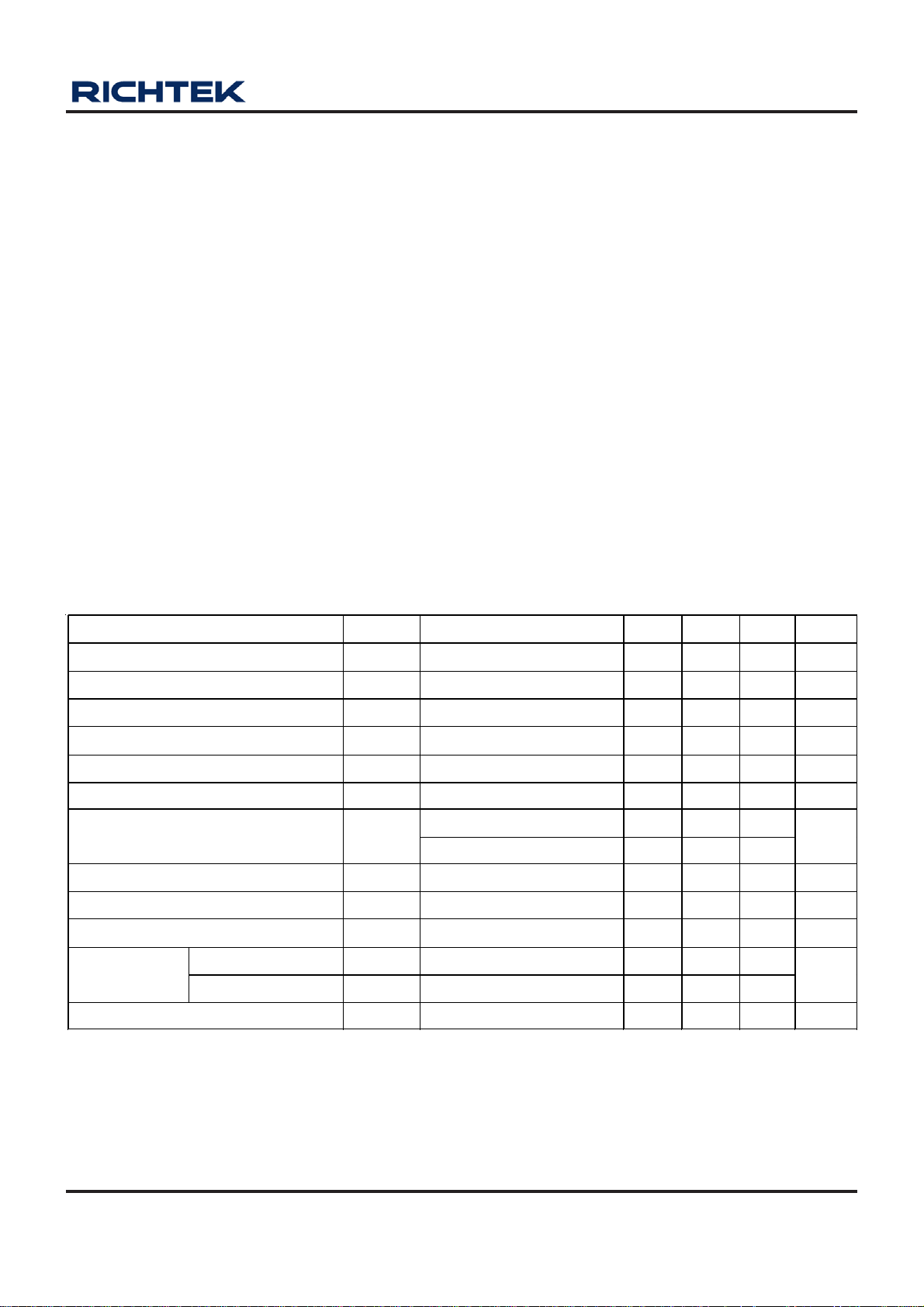
Electrical Characteristics
(V
= V
IN
+ 0.7V, I
OUT
Parameter Symbol Test Conditions Min Typ Max Unit
Reference Voltage Tolerance V
Adjust Pin Current I
Output Voltage Range V
Quiescent Current (Note 5) IQ Enabled, I
Standby Current (Note 6) I
Current Limit I
Dropout Voltage (Note 7) V
Line Regulation ΔV
Thermal Shutdown Temperature TSD -- 170 -- °C
Thermal Shutdown Hysteresis ΔTSD -- 40 -- °C
EN Threshold
EN Current IEN V
= 10uA, C
OUT
Logic-Low Voltage VIL V
Logic-High Voltage V
= C
IN
= 1uF (Ceramic), T
OUT
1.163 1.175 1.187 V
REF
-- -- 10 nA
ADJ
1.175 -- 4.5 V
OUT
VIN = 5.5V, Shutdown -- -- 1 μA
STBY
0.5 -- -- A
LIM
DROP
V
LINE
V
IH
= 25°C unless otherwise specified)
A
I
= 10mA -- 10 --
OUT
= 300mA -- 300 -
I
OUT
+ 0.7V < VIN < 5.5V -- 0.001 -- %/V
OU T
= 3.3V, Shutdown -- -- 0.4
IN
= 3.3V, Enable 2.0 -- --
IN
= 5.5V, Enable -- -- 10 nA
IN
= 0mA -- 150 -- μA
OUT
mV
V
DS9179-11 April 2011 www.richtek.com
3

RT9179
Note 1. Stresses listed as the above "Absolute Maximum Ratings" may cause permanent damage to the device. These are for
stress ratings. Functional operation of the device at these or any other conditions beyond those indicated in the
operational sections of the specifications is not implied. Exposure to absolute maximum rating conditions for extended
periods may remain possibility to affect device reliability.
Note 2. θ
Note 3. Devices are ESD sensitive. Handling precaution is recommended.
Note 4. The device is not guaranteed to function outside its operating conditions.
Note 5. Quiescent, or ground current, is the difference between input and output currents. It is defined by I
Note 6. Standby current is the input current drawn by a regulator when the output voltage is disabled by a shutdown signal
(V
Note 7. The dropout voltage is defined as V
is measured in the natural convection at TA = 25°C on a low effective thermal conductivity test board of
JA
JEDEC 51-3 thermal measurement standard.
= IIN - I
Q
no load condition (I
= 0mA). The total current drawn from the supply is the sum of the load current plus the ground
OUT
pin current.
0.4V). It is measured with V
EN
≤
= 5.5V.
IN
IN
-V
, which is measured when V
OUT
OUT
is V
OUT(NORMAL)
− 100mV.
OUT
under
DS9179-11 April 2011www.richtek.com
4
 Loading...