Preliminary
RT9177
Ultra-Low-Noise 200mA LDO Regulator
General Description
The RT9177 is a 200mA low dropout and low noise
micro-power regulator suitable for portable RF
applications. The output voltage accuracy is within
±2% and range from 2.4V to 3.2V in 100mV
increments could be selected. It is designed for
using very low ESR output capacitor. Its output
remains stable even when using a 1µF ceramic as
its output capacitor.
With an internal PMOS as the pass device, it does
not need extra GND current in heavy load and
dropout conditions. In shutdown mode, nearly zero
operation current makes the IC suitable for battery-
power devices. Other features including current
limiting and over temperature protection. The noise
performance can be improved by connecting a
capacitor to the bypass pin.
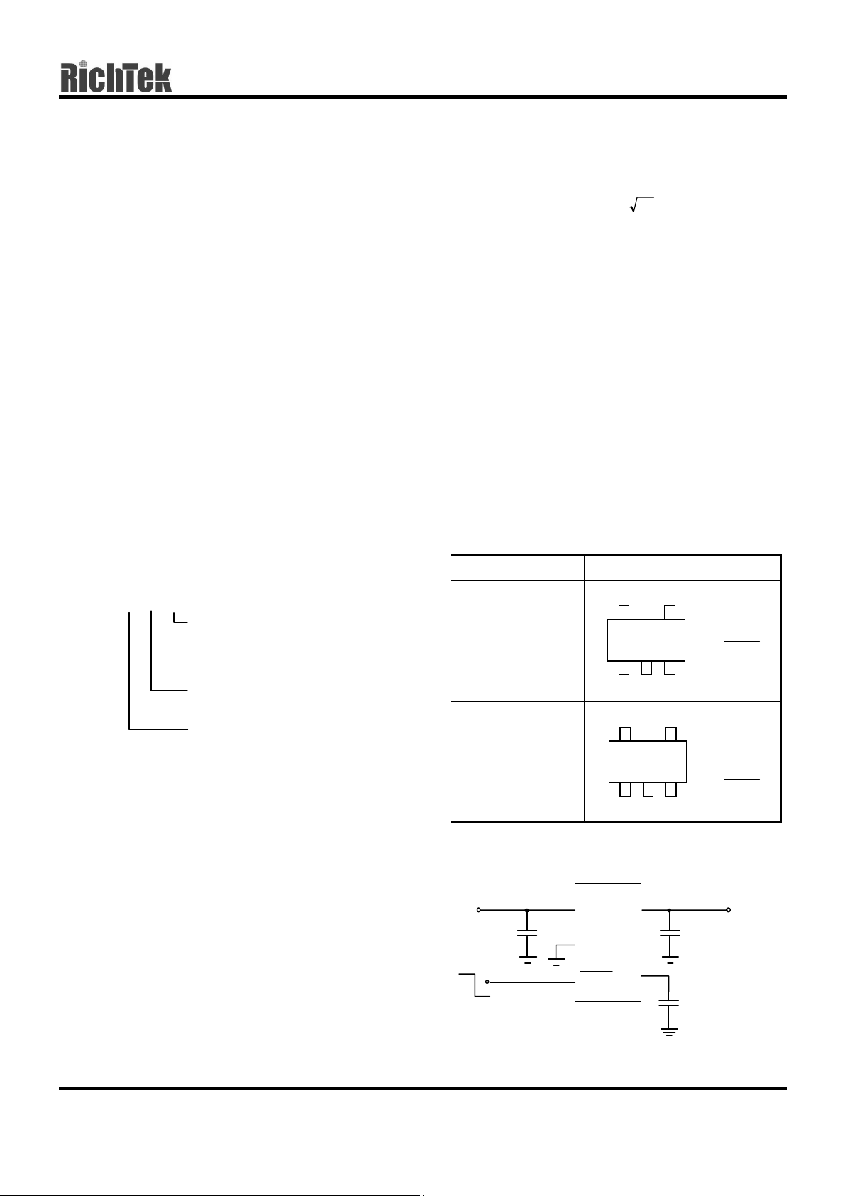
Ordering Information
RT9177-
Package type
B
: SOT-25 Type I
BR : SOT-25 Type II
Operating temperature range
C : Commercial standard
Output voltage
24 : 2.4V
25 : 2.5V
:
:
Features
z
Ultra-Low-Noise (150nV/
z
1µµµµF Ceramic C
Low Dropout Voltage (220mV @ 200mA)
z
Low Operation Current - 80µµµµA Typical
z
Shutdown Function
z
Low Temperature Coefficient
z
Current and Thermal Limiting
z
Customized Voltage Available
z
SOT-25 Package
z
OUT
Stable
) for RF Application
Hz
Applications
z Cellular Phones
z Laptop, Notebook, and Palmtop Computers
z Battery-powered Equipment
z Hand-held Equipment
Pin Configurations
Part Number Pin Configurations
321
TOP VIEW
1. IN
2. GND
3. SHDN
4. BP
5. OUT
TOP VIEW
1. OUT
2. GND
3. IN
4. SHDN
5. BP
RT9177-CB
(Plastic SOT-25)
RT9177-CBR
(Plastic SOT-25)
54
321
54
31 : 3.1V
32 : 3.2V
DS9177-02 June 2001 www.richtek-ic.com.tw
Typical Application Circuit
RT9177
V
IN
ON
OFF
C
IN
1µF
IN
OUT
GND
SHDN BP
C
1µF
C
10nF
OUT
BP
V
OU T
1

RT9177
Marking Information
Preliminary
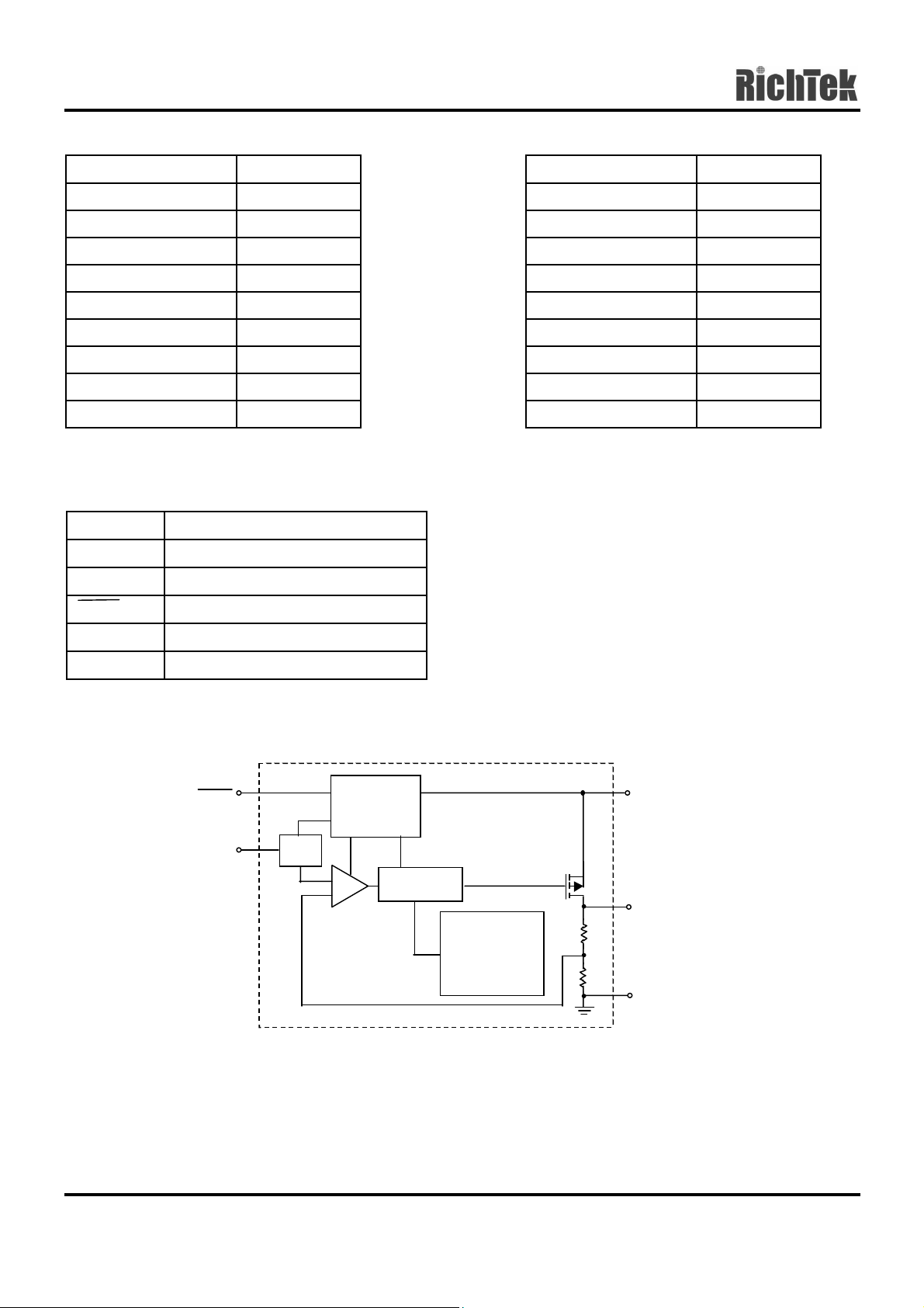
Part Number Marking
RT9177-24CB H9
RT9177-25CB HA
RT9177-26CB HB
RT9177-27CB HC
RT9177-28CB HD
RT9177-29CB HE
RT9177-30CB HF
RT9177-31CB HG
RT9177-32CB HH
Pin Description
Pin Name Pin Function
IN Input
GND Ground
SHDN Active Low Shutdown Input
Part Number Marking
RT9177-24CBR P9
RT9177-25CBR PA
RT9177-26CBR PB
RT9177-27CBR PC
RT9177-28CBR PD
RT9177-29CBR PE
RT9177-30CBR PF
RT9177-31CBR PG
RT9177-32CBR PH
BP Reference Noise Bypass
OUT Output
Function Block Diagram
SHDN
BP
VREF
Shutdown
Logic Control
+
_
Error Amp
and
MOS Driver
IN
OUT
Current-Limit
and
Thermal
Protection
GND
www.richtek-ic.com.tw DS9177-02 June 2001
2

Absolute Maximum Ratings
Preliminary
RT9177
Input Voltage
z
Power Dissipation, PD @ TA = 25°C
z
7V
SOT-25 0.25W
Operating Junction Temperature Range −40°C to 125°C
z
Storage Temperature Range −65°C to 150°C
z
Package Thermal Resistance
z
SOT-25, θ
Lead Temperature (Soldering, 5 sec.) 260°C
z
JA
250°C/W
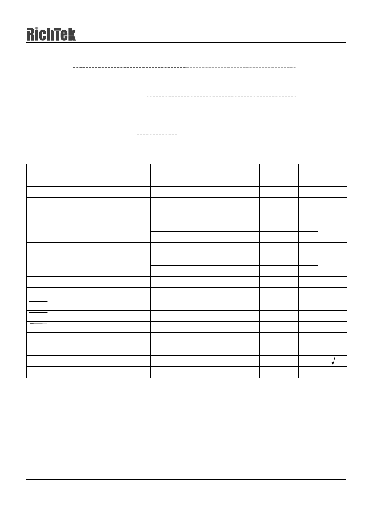
Electrical Characteristics
(V
= 5.0V, C
IN
Input Voltage Range
Output Voltage Accuracy
Maximum Output Current
Current Limit
GND Pin Current
Dropout Voltage
(V
(Nominal)≥3.0V Version)
OUT
Line Regulation
Load Regulation
SHDN Input High Threshold
SHDN Input Low Threshold
SHDN Bias Current
Shutdown Supply Current
Thermal Shutdown Temperature
Output Noise
Ripple Rejection PSRR
Notes: Dropout voltage definition: V
= 1µF, C
IN
OUT
= 1µF, T
= 25°C, unless otherwise specified)
A
Parameter Symbol Test Conditions Min Typ Max Units
V
IN
∆V
OUTIL
I
MAX
I
LIMIT
= 1mA
R
LOAD
= 1Ω
2.5 -- 6 V
-2 -- +2 %
200 -- -- mA
-- 300 -- mA
No Load -- 80 150
I
(Note)
G
V
DROP
∆V
LINEVIN
∆V
LOADIOUT
V
IH
V
IL
I
SD
I
GSD
T
SD
e
NO
- V
IN
OUT
I
= 200mA
OUT
I
= 1mA
OUT
I
= 50mA
OUT
I
= 200mA
OUT
= (V
+0.15) to 6V, I
OUT
= 0mA to 200mA
VIN = 3V to 5.5V
VIN = 3V to 5.5V
V
= 0V
OUT
CBP = 10nF, C
F = 100Hz, C
when V
is 50 mV below the value of V
OUT
= 10µF
OUT
= 10nF, C
BP
OUT
OUT
= 1mA
= 10µF
-- 90 150
-- 1.1 5
-- 55 100
-- 220 300
-0.2 -- +0.2 %/V
-- 0.01 0.04 %/mA
1.0 -- -- V
-- -- 0.4 V
-- -- 100 nA
-- 0.01 1
-- 150 --
-- 150 --
nV/
-- 68 --
OUT
at V
IN
= V
OUT
+ 0.5V
µA
mV
µA
°C
Hz
dB
DS9177-02 June 2001 www.richtek-ic.com.tw
3

RT9177
0
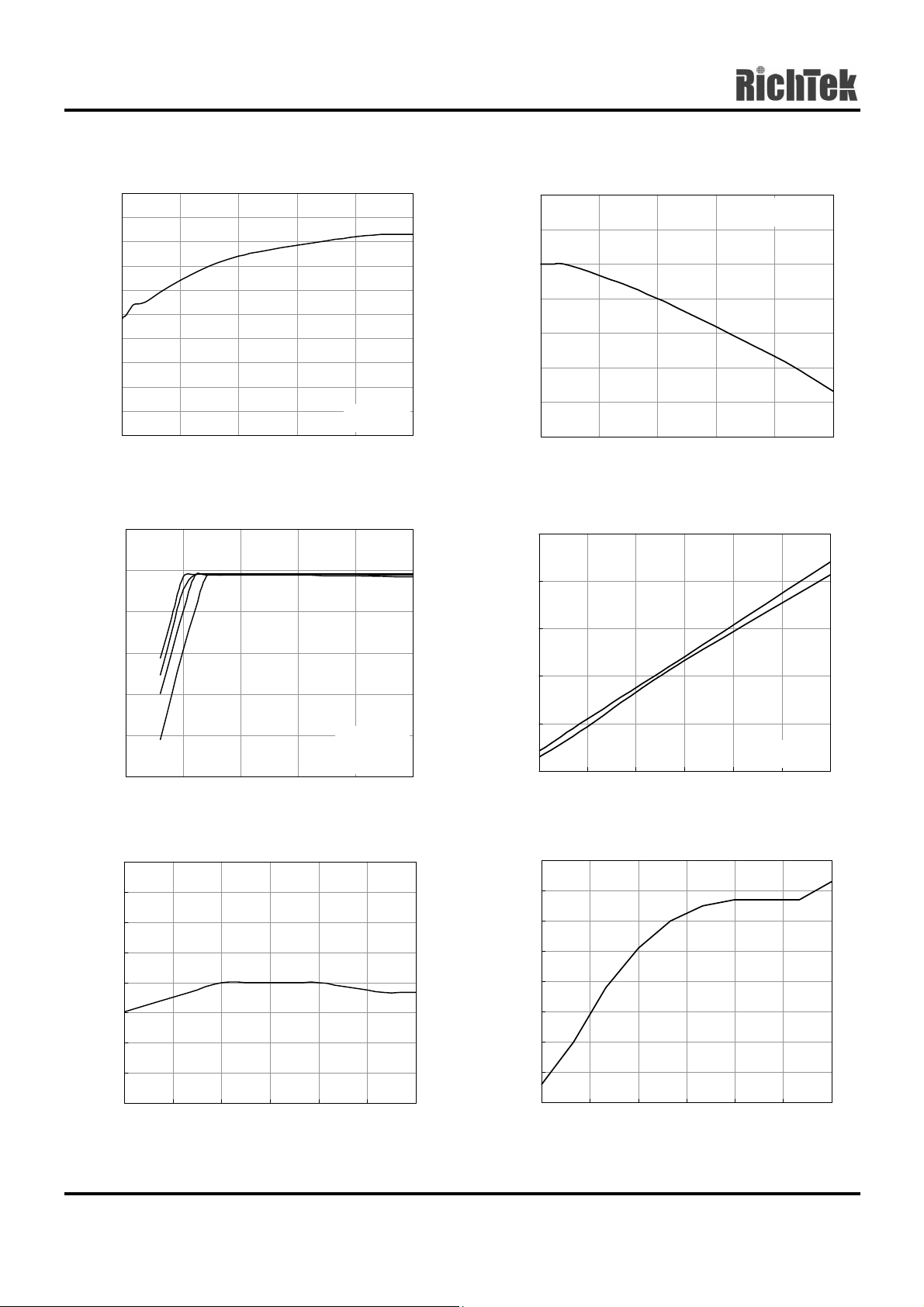
Typical Operating Characteristics
Preliminary
75
GND Current vs. Load
74
73
72
71
70
(uA)
G
I
69
68
67
66
65
0 50 100 150 200 250
I
(mA)
OUT
V
vs. V
3.10
3.00
2.90
(V)
2.80
20mA
OUT
V
50mA
2.70
100mA
2.60
2.50
200mA
2.5 3.0 3.5 4.0 4.5 5.0
OUT
VIN (V)
IN
TA = 25°C
V
OUT
T
A
= 3V
= 25°C
Output Voltage Variation vs. Load
0.2
0.1
0.0
-0.1
(%)
OUT
-0.2
V
∆
-0.3
-0.4
-0.5
0 50 100 150 200 25
I
OUT
(mA)
Dropout Voltage vs. Output Current
250
200
150
100
Dropout Voltage (mV)
50
0
20 50 80 110 140 170 200
Output Current (mA)
TA = 25°C
80 C
25 C
V
= 3V
OUT
°
°
Output Voltage Variation vs. Temperature
1.00
0.75
0.50
0.25
(%)
0.00
OUT
V
-0.25
-0.50
-0.75
-1.00
-40 -10 20 50 80 110 140
Temperature ( C)
°
No Load
71
70
69
68
67
(uA)
G
I
66
65
64
63
GND Current vs. Tem perature
-40 -10 20 50 80 110 140
Temperature ( C)
°
www.richtek-ic.com.tw DS9177-02 June 2001
4
 Loading...