Preliminary
RT9174
Triple Linear Regulator Controllers
General Description
The RT9174 is a triple linear regulator controller
designed for motherboard application.
The regulators are intended to regulate the
computer system AGP (2X/4X) power, the 2.5V
clock power, and the 1.8V power for North/South
Bridge core voltage and/or cache memory circuits.
All controllers can drive NPN or NMOSFET pass
transistor. A special scheme empoly driver voltage
could be higher than V
when driving NMOSFET
DD
through the 12V power.
The RT9174 future a small SOP-8 package for
saving board area. It also builds in current limiting
and thermal shutdown protection function.
Ordering Information
RT9174C S
Package type
S : SOP-8
Operating temperature range
C: Commercial standard
Features
z
Integrated Three Linear Controllers in a SOP-8
Package
z
Driving NPN or NMOSFET
z
Sourcing ( > 100mA) and Sinking ( > 5mA) Driver
z
Tri-State Output Driver
z
Low Internal 0.8V Reference
z
Adjustable Output Voltage Setting
z
High Output Stability
z
V
1.5/3.3V Automatic Changing for AGP
DDQ
z
Wide 3V ~ 8V Input Voltage Range
z
Current Limiting and Thermal Protection
Applications
Mother Boards Power Supply
z
Graphic Cards
z
Pin Configurations
Part Number Pin Configurations
RT9174CS
(Plastic SOP-8)
VDD
DRI 1
TOP VIEW
1
2
DRI 3
8
FB3
7
Function Block Diagram
VDD
DRI1
FB1
GND
Thermal
Limit
OC
+
_
_
+
0.8V 1.3 V
Referenc e
DRI 2
3
FB1
4
GND
OC
+
_
_
+
OC
+
_
_
+
DRI2
FB2
DRI3
FB3
6
FB2
5
DS9174-00 April 2001 www.richtek-ic.com.tw
1

RT9174
Preliminary
Pin Description
Pin Name Pin Function
VDD Power Supply Input
DRI1 Regulator 1 Driver Output
FB1 Regulator 1 Feedback Non-inverting Input
GND Ground
DRI2 Regulator 2 Driver Output
FB2 Regulator 2 Feedback Non-inverting Input
DRI3 Regulator 3 Driver Output
FB3 Regulator 3 Feedback Non-inverting Input
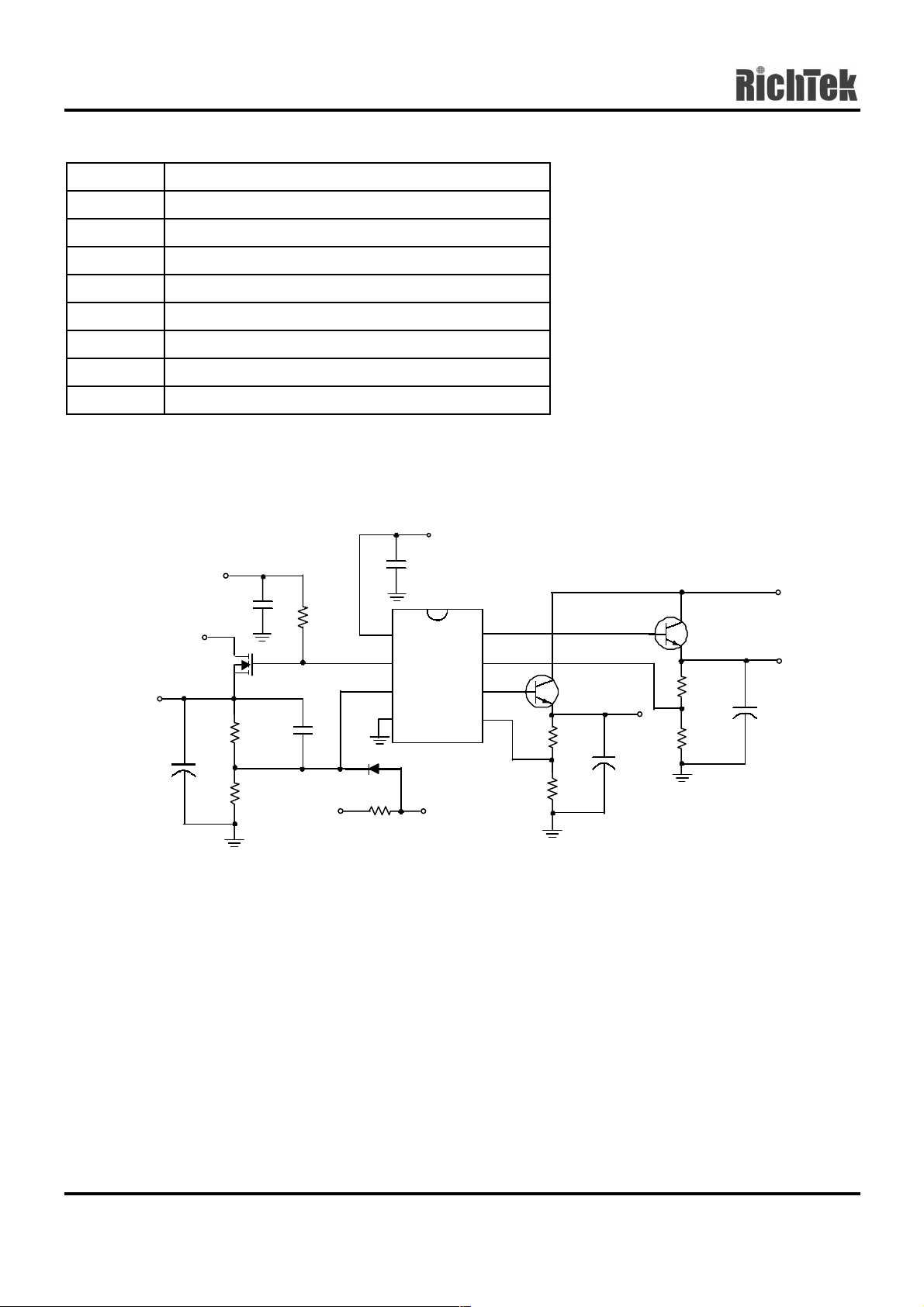
Typical Application Circuit
C
1
1µF
1
VDD
2
DRI1
3
FB1
4
GND
RT9174
1
8
V
DDQ
1.5/ 3.3V
1000µF
12V
3.3V
PHD4 5N03 LT
C
+
2
0.1µF
Q
1
C
5
R
4.3K
R
4.99K
R
1
5K
2
3
C6
10nF
D
1N4148
R
1K
#TYPEDET3.3V
5V
DRI3
FB3
DRI2
FB2
3.3V
8
7
6
5
Q
2
2SD1802
R
4
250
+
R
5
200
V
O2
1.8V
C
3
470µF
Q
3
2SD1802
R
6
424
R
7
200
V
O3
2.5V
+
C
4
470µF
VDDQ = 3.3V if FB1 >1.3V
#TYPEDET = 0V →VDDQ = 1.5V
#TYPEDET = Open →VDDQ = 3.3V
Fig 1. Triple LDOs with VDDQ fo r M/B Application
www.richtek-ic.com.tw DS9174-00 April 2001
2

12V
C
5
0.1µF
3.3V
Q
PHD4 5N03LT
V
DDQ
1.5/ 3.3V
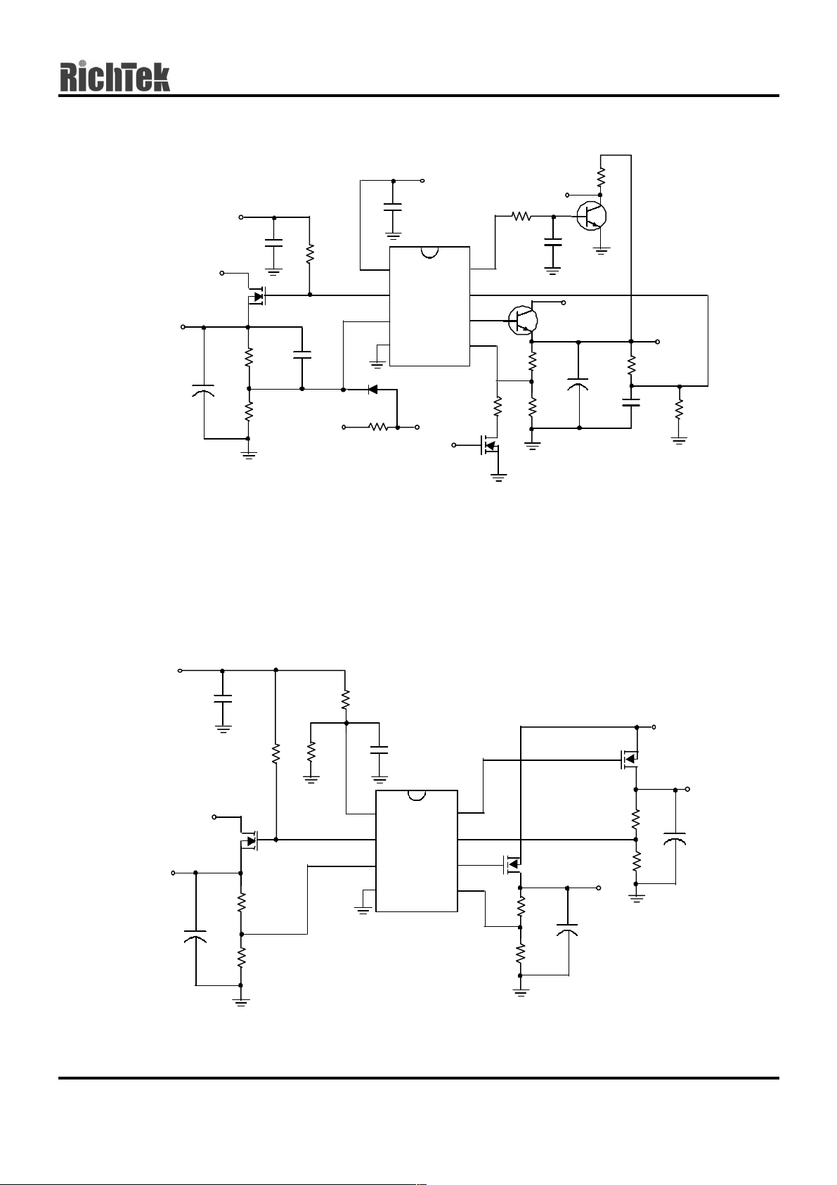
VDDQ = 3.3V if FB1 > 1.3V
#TYPEDET = 0V →VDDQ = 1.5V
#TYPEDET = Open →VDDQ = 3.3V
VTTSEL = 0V →VTT = 1. 2 5V
VTTSEL = 5V →VTT = 1. 5 V
1
R
2
+
4.3K
R
3
4.99K
R
1
5K
C6
10nF
Preliminary
C
1
1µF
1
VDD
2
DRI1
3
FB1
4
GND
RT91 74
D
1
1N4148
R
8
1K
#TYPEDET3.3V
5V
DRI3
FB3
DRI2
FB2
V
TTSEL
RT9174
R
V
TTPG
R
10
1K
C
8
7
6
5
R
11
374
Q
4
2N7002
8
0.01µF
3.3V
Q
2
2SD1802
R
4
113
+
R
5
200
1K
C
3
470µF
9
Q
MMBT39 04
R
3K
C
1µF
3
V
TT
6
7
R
12
8.2K
12V
PHD4 5N 03L T
V
O1
3.3V
C
2
1000µF
Fig 2. Dual LDOs with V
R
3K
R
9
1.2K
7.5V
C
8
1
1µF
1
VDD
2
DRI1
3
FB1
4
GND
DRI3
FB3
DRI2
FB2
RT9174
C
5
0.1µF
R
1
5K
5V
Q
1
R
2
+
624
R
200
3
for VRM8.5 Application
TTPG
8
7
6
5
Q
2
PHD4 5N 03L T
R
250
R
200
3.3V
Q
3
PHD4 5N 03L T
V
O3
R
424
R
O2
200
V
4
5
1.8V
+
C
3
470µF
2.5V
6
+
C
4
470µF
7
Fig 3. T ripl e LD Os Driving MOS Applicat ion
DS9174-00 April 2001 www.richtek-ic.com.tw
3
 Loading...