

Page 1
RT9173C
Cost-Effective, 2A Sink/Source Bus Termination Regulator
General Description
The RT9173C is a simple, cost-effective and high-speed
linear regulator designed to generate termination voltage
in double data rate (DDR) memory system to comply with
the JEDEC SSTL_2 and SSTL_18 or other specific
interfaces such as HSTL, SCSI-2 and SCSI-3 etc. devices
requirements. The regulator is capable of actively sinking
or sourcing up to 2A while regulating an output voltage to
within 40mV. The output termination voltage cab be tightly
regulated to track 1/2V
by two external voltage divider
DDQ
resistors or the desired output voltage can be pro-grammed
by externally forcing the REFEN pin voltage.
The RT9173C also incorporates a high-speed differential
amplifier to provide ultra-fast response in line/load transient.
Other features include extremely low initial offset voltage,
excellent load regulation, current limiting in bi-directions
and on-chip thermal shut-down protection.
The RT9173C are available in the SOP-8 (Exposed Pad)
surface mount packages.
Ordering Information
RT9173C
Package Type
SP : SOP-8 (Exposed Pad-Option 1)
Lead Plating System
P : Pb Free
G : Green (Halogen Free and Pb Free)
Note :
Richtek products are :
` RoHS compliant and compatible with the current require-
ments of IPC/JEDEC J-STD-020.
` Suitable for use in SnPb or Pb-free soldering processes.
Features
zz
Ideal for DDR-I, DDR-II and DDR-III V
z
zz
zz
z Sink and Source 2A Continuous Current
zz
zz
z Integrated Power MOSFETs
zz
zz
z Generates Termination Voltage for SSTL_2,
zz
Applications
TT
SSTL _18, HSTL, SCSI-2 and SCSI-3 Interfaces
zz
z High Accuracy Output Voltage at Full-Load
zz
zz
z Output Adjustment by Two External Resistors
zz
zz
z Low External Component Count
zz
zz
z Shutdown for Suspend to RAM (STR) Functionality
zz
with High-Impedance Output
zz
z Current Limiting Protection
zz
zz
z On-Chip Thermal Protection
zz
zz
z Available in SOP-8 (Exposed Pad) Packages
zz
zz
z V
and V
zz
IN
zz
z RoHS Compliant and 100% Lead (Pb)-Free
zz
No Power Sequence Issue
CNTL
Applications
z Desktop PCs, Notebooks, and Workstations
z Graphics Card Memory Termination
z Set Top Boxes, Digital TVs, Printers
z Embedded Systems
z Active Termination Buses
z DDR-I, DDR-II and DDR-III Memory Systems
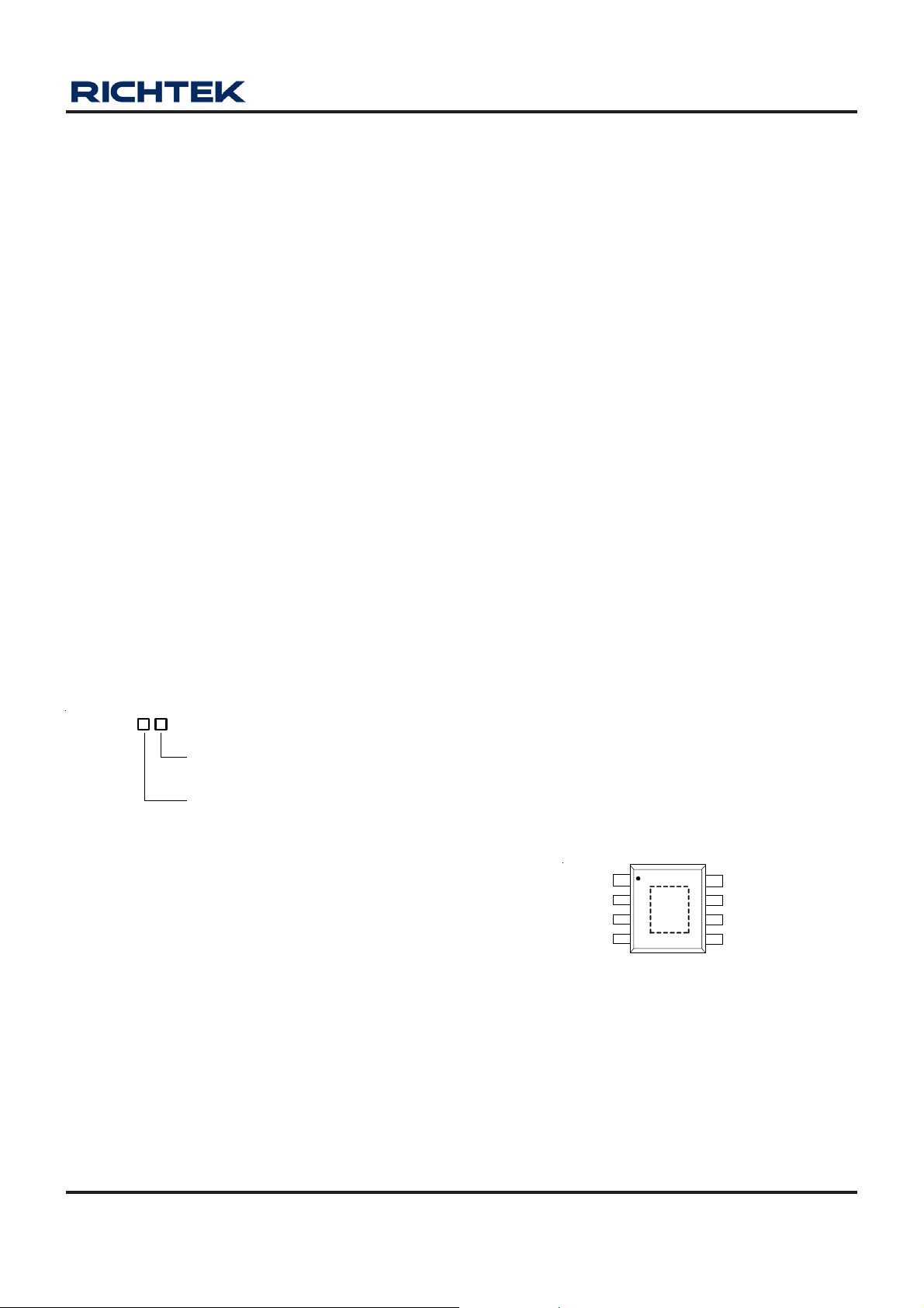
Pin Configurations
(TOP VIEW)
GND
8
NC
7
NC
6
9
VCNTL
5
NC
VIN
GND
REFEN
VOUT
2
3
4
SOP-8 (Exposed Pad)
DS9173C-13 April 2011 www.richtek.com
1
Page 2
RT9173C
Typical Application Circuit
V
= 3.3V
CNTL
VIN = 2.5V/1.8V/1.5V
2N7002
EN
R1 = R2 = 100kΩ, RTT = 50Ω / 33Ω / 25Ω
C
OUT(MIN)
CSS = 1μF, CIN = 470μF (Low ESR), C
Functional Pin Description
= 10μF (Ceramic) + 1000μF under the worst case testing condition
R
TT
R
1
R
C
2
CNTL
REFEN
SS
= 47μF
VIN
RT9173C
GND
GND
VCNTL
VOUT
C
C
CNTL
IN
C
OUT
VIN (Pin 1)
Input voltage which supplies current to the output pin. Connect this pin to a well-decoupled supply voltage. To prevent the
input rail from dropping during large load transient, a large, low ESR capacitor is recommended to use. The capacitor
should be placed as close as possible to the VIN pin.
GND [Pin 2, Exposed pad (9)]
Common Ground (Exposed pad is connected to GND). The GND pad area should be as large as possible and using many
vias to conduct the heat into the buried GND plate of PCB layer.
VCNTL (Pin 6)
VCNTL supplies the internal control circuitry and provides the drive voltage. The driving capability of output current is
proportioned to the VCNTL. Connect this pin to 3.3V bias supply to handle large output current with at least 10μF
capacitor from this pin to GND.
REFEN (Pin 3)
Reference voltage input and active low shutdown control pin. Two resistors dividing down the VIN voltage on the pin to
create the regulated output voltage. Pulling the pin to ground turns off the device by an open-drain, such as 2N7002,
signal N-Channel MOSFET.
VOUT (Pin 4)
Regulator output. VOUT is regulated to REFEN voltage that is used to terminate the bus resistors. It is capable of sinking
and sourcing current while regulating the output rail. To maintain adequate large signal transient response, typical value
of 1000μF AL electrolytic capacitor with 10μF ceramic capacitors are recommended to reduce the effects of current
transients on VOUT.
NC (Pin 5, 7, 8)
No Internal Connect.
DS9173C-13 April 2011www.richtek.com
2
Page 3
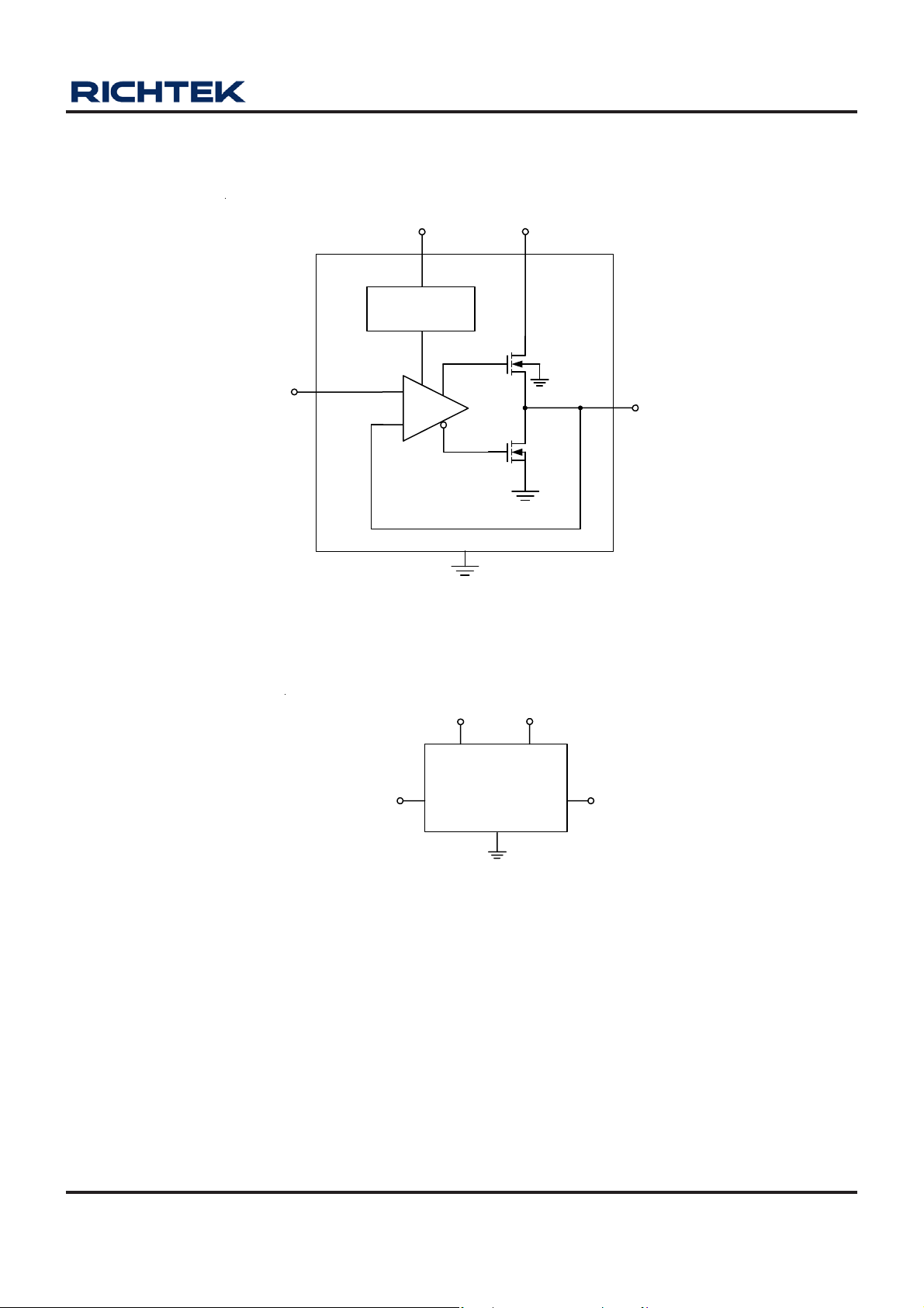
Function Block Diagram
RT9173C
REFEN
VCNTL
Current Limit
Thermal Protection
+
EA
-
GND
VIN
VOUT
Test Circuit
2.5V/1.8V/1.5V 3.3V
1.25V/0.9V/0.75V
VIN
REFEN
VCNTL
RT9173C
GND
VOUT
V
OUT
Figure 1. Test Circuit for Typical Operating Characteristics Curves
DS9173C-13 April 2011 www.richtek.com
3
Page 4
RT9173C
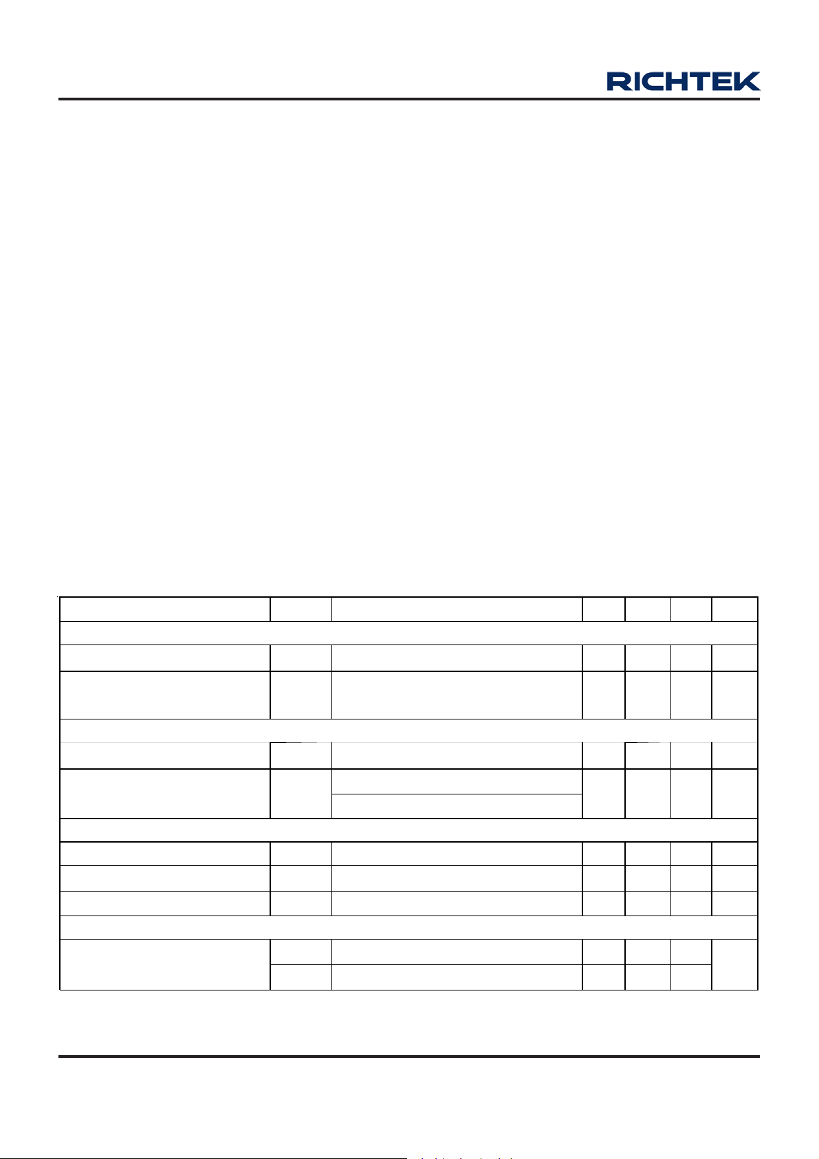
Absolute Maximum Ratings (Note 1)
z Input Voltage, V
z Control Voltage, V
z Power Dissipation, P
---------------------------------------------------------------------------------------------------- 6V
IN
---------------------------------------------------------------------------------------------- 6V
CNTL
@ TA = 25°C
D
SOP-8 (Exposed Pad) ---------------------------------------------------------------------------------------------- 1.33W
z Package Thermal Resistance (Note 2)
SOP-8 (Exposed Pad), θJA---------------------------------------------------------------------------------------- 75°C/W
SOP-8 (Exposed Pad), θJC---------------------------------------------------------------------------------------- 28°C/W
z Junction Temperature ----------------------------------------------------------------------------------------------- 125°C
z Lead Temperature (Soldering, 10 sec.) ------------------------------------------------------------------------- 260°C
z Storage Temperature Range --------------------------------------------------------------------------------------- –65°C to 150°C
z ESD Susceptibility (Note 3)
HBM (Human Body Mode) ----------------------------------------------------------------------------------------- 2kV
MM (Machine Mode) ------------------------------------------------------------------------------------------------ 200V
Recommended Operating Conditions (Note 4)
z Input Voltage, V
z Control Voltage, V
z Ambient Temperature Range -------------------------------------------------------------------------------------- −40°C to 85°C
z Junction Temperature Range -------------------------------------------------------------------------------------- −40°C to 125°C
---------------------------------------------------------------------------------------------------- 2.5V to 1.5V ± 3%
IN
---------------------------------------------------------------------------------------------- 5V or 3.3V ± 5%
CNTL
Electrical Characteristics
(V
= 2.5V/1.8V/1.5V, V
IN
Parameter Symbol Test Conditions Min Typ Max Unit
Input
V
Operation Current I
CNTL
Standby Current (Note 7) I
Output (DDR / DDR II / DDR III)
Output Offset Voltage (Note 5) VOS I
Load Regulation (Note 6) ΔV
Protection
Current limit I
Thermal Shutdown Temperature TSD 3.3V ≤ V
Thermal Shutdown Hysteresis ΔTSD 3.3V ≤ V
REFEN Shutdown
Sh utdown T h resh old
CNTL
= 3.3V, V
= 1.25V/0.9V/0.75V, C
REFEN
I
CNTL
STB Y
LOAD
2.2 -- -- A
LIM
= 0A -- 1 2.5 mA
OUT
V
REFEN
R
LOAD
= 0A −20 -- +20 mV
OUT
I
= 2A
OUT
I
= −2A
OUT
VIH Enable 0.6 -- --
V
Shutdown -- -- 0.2
IL
= 10μF (Ceramic), T
OUT
< 0.2V (Shutdown),
= 180Ω
= 25°C, unless otherwise specified)
A
-- 50 90 μA
−20 -- +20 mV
≤ 5V 125 170 -- °C
CNTL
≤ 5V -- 35 -- °C
CNTL
V
DS9173C-13 April 2011www.richtek.com
4
Page 5

RT9173C
Note 1. Stresses listed as the above "Absolute Maximum Ratings" may cause permanent damage to the device. These are for
stress ratings. Functional operation of the device at these or any other conditions beyond those indicated in the
operational sections of the specifications is not implied. Exposure to absolute maximum rating conditions for extended
periods may remain possibility to affect device reliability.
Note 2. θJA is measured in the natural convection at TA = 25°C on a high effective thermal conductivity test board (4 Layers,
2S2P) of JEDEC 51-7 thermal measurement standard. The case point of θ
Pad) package.
Note 3. Devices are ESD sensitive. Handling precaution recommended.
Note 4. The device is not guaranteed to function outside its operating conditions.
Note 5. V
offset is the voltage measurement defined as V
OS
subtracted from V
OUT
Note 6. Regulation is measured at constant junction temperature by using a 5ms current pulse. Devices are tested for load
regulation in the load range from 0A to 2A.
Note 7. Standby current is the input current drawn by a regulator when the output voltage is disabled by a shutdown signal on
REFEN pin (V
< 0.2V). It is measured with VIN = V
IL
CNTL
= 5V.
is on the expose pad for SOP-8 (Exposed
JC
.
REFEN
DS9173C-13 April 2011 www.richtek.com
5
Page 6

RT9173C
Typical Operating Characteristics
0.77
VIN = 1.5V
0.765
0.76
0.755
0.75
Output Voltage (V)
0.745
0.74
-50 -25 0 25 50 75 100 125
Tempe rature
(°C)
Output Voltage vs. Temperature
1.27
VIN = 2.5V
1.265
1.26
1.255
1.25
Output Voltage (V)
1.245
Output Voltage vs. Temperature
Output Voltage vs. Temperature
0.92
VIN = 1.8V
0.915
0.91
0.905
0.9
Output Voltage (V)
0.895
0.89
-50-25 0 255075100125
Temperature
(°C)
Shutdown Threshold vs. Temperature
0.6
V
= 5V, Turn On
0.55
0.5
0.45
0.4
V
0.35
Shutdown Threshold (V)
0.3
CNTL
= 3.3V, Turn On
CNTL
V
CNTL
V
CNTL
= 3.3V, Turn Off
= 5V, Turn Off
1.24
-50-25 0 25 50 75100125
Temperature
(°C)
VIN Current vs. Temperature
5
4.5
VIN = 2.5V, V
VIN = 2.5V, V
4
3.5
Current (mA)
3
IN
V
2.5
2
-50 -25 0 25 50 75 100 125
VIN = 1.8V, V
VIN = 1.8V, V
= 3.3V
CNTL
= 5V
CNTL
VIN = 1.5V, V
VIN = 1.5V, V
Temperature
CNTL
CNTL
= 5V
CNTL
= 3.3V
= 5V
CNTL
(°C)
= 3.3V
0.25
-50-25 0 255075100125
Temperature
(°C)
Vcntl Current vs. Temperature
0.6
0.55
0.5
0.45
0.4
Vcntl Current (mA)
0.35
0.3
VIN = 2.5V, V
VIN = 2.5V, V
VIN = 1.5V, V
-50-25 0 25 50 75100125
VIN = 1.8V, V
VIN = 1.8V, V
= 3.3V
CNTL
= 5V
CNTL
CNTL
VIN = 1.5V, V
Temperature
CNTL
= 5V
CNTL
CNTL
= 5V
= 3.3V
(°C)
= 3.3V
DS9173C-13 April 2011www.richtek.com
6
Page 7

RT9173C
Source Current Limit vs. Temperature
4.5
VIN = 1.8V, V
VIN = 1.8V, V
4
VIN = 2.5V, V
VIN = 2.5V,
V
= 3.3V
CNTL
3.5
3
2.5
Source Current Limit (A)
2
-50 -25 0 25 50 75 100 125
CNTL
CNTL
= 5V
= 3.3V
Temperature
= 5V
CNTL
VIN = 1.5V, V
VIN = 1.5V, V
(°C)
0.9VTT @ 2A Transient Response
40
20
Output Voltage
Transient (mV)
-20
VIN = 1.8V, V
0
CNTL
= 3.3V, V
OUT
= 0.9V
CNTL
CNTL
= 5V
= 3.3V
Sink
Sink Current Limit vs. Temperature
4.5
4
VIN = 2.5V, V
VIN = 1.8V, V
3.5
3
Sink Current Limit (A)
2.5
VIN = 1.5V, V
2
-50-25 0 25 50 75100125
VIN = 1.8V, V
VIN = 2.5V, V
CNTL
= 5V
CNTL
CNTL
VIN = 1.5V, V
Temperature
CNTL
= 5V
= 5V
CNTL
CNTL
= 3.3V
= 3.3V
= 3.3V
(°C)
0.9VTT @ 2A Transient Response
40
20
Output Voltage
Transient (mV)
-20
VIN = 1.8V, V
0
CNTL
= 3.3V, V
OUT
= 0.9V
Source
2
1
(A)
0
Output Current
Swing Frequency : 1kHz
0.75VTT @ 2A Transient Response
VIN = 1.5V, V
40
20
0
Output Voltage
Transient (mV)
-20
2
1
(A)
0
Output Current
Swing Frequency : 1kHz
Time (250μs/Div)
= 3.3V, V
CNTL
OUT
= 0.75V
Sink
2
1
(A)
0
Output Current
Swing Frequency : 1kHz
0.75VTT @ 2A Transient Response
VIN = 1.5V, V
40
20
0
Output Voltage
Transient (mV)
-20
2
1
(A)
0
Output Current
Swing Frequency : 1kHz
Time (250μs/Div)
= 3.3V, V
CNTL
OUT
= 0.75V
Source
Time (250μs/Div)
Time (250μs/Div)
DS9173C-13 April 2011 www.richtek.com
7
Page 8

RT9173C
1.25VTT @ 2A Transient Response
VIN = 2.5V, V
40
20
0
Output Voltage
Transient (mV)
-20
2
1
(A)
0
Output Current
Swing Frequency : 1kHz
Output Short-Circuit Protection
VIN = 1.5V, V
12
10
8
= 3.3V, V
CNTL
OUT
Time (250μs/Div)
= 3.3V
CNTL
= 1.25V
Sink
Sink
1.25VTT @ 2A Transient Response
VIN = 2.5V, V
40
20
0
Output Voltage
Transient (mV)
-20
2
1
(A)
0
Output Current
Swing Frequency : 1kHz
Output Short-Circuit Protection
VIN = 1.5V, V
12
10
8
= 3.3V, V
CNTL
Time (250μs/Div)
= 3.3V
CNTL
OUT
= 1.25V
Source
Source
6
4
2
Output Short Circuit (A)
0
Output Short-Circuit Protection
VIN = 1.8V, V
12
10
8
6
4
2
Output Short Circuit (A)
0
CNTL
Time (1ms/Div)
= 3.3V
Sink
6
4
2
Output Short Circuit (A)
0
Output Short-Circuit Protection
VIN = 1.8V, V
12
10
8
6
4
2
Output Short Circuit (A)
0
CNTL
Time (1ms/Div)
= 3.3V
Source
Time (1ms/Div)
Time (1ms/Div)
DS9173C-13 April 2011www.richtek.com
8
Page 9

RT9173C
Output Short-Circuit Protection
VIN = 2.5V, V
12
10
8
6
4
2
Output Short Circuit (A)
0
CNTL
= 3.3V
Time (1ms/Div)
Sink
Output Short-Circuit Protection
VIN = 2.5V, V
12
10
8
6
4
2
Output Short Circuit (A)
0
CNTL
= 3.3V
Time (1ms/Div)
Source
DS9173C-13 April 2011 www.richtek.com
9
Page 10

RT9173C
Application Information
Consideration while designs the resistance of voltage
divider
Make sure the sinking current capability of pull-down NMOS
if the lower resistance was chosen so that the voltage on
V
is below 0.2V.
REFEN
In addition, the capacitor and voltage divider form the low-
pass filter. There are two reasons doing this design; one is
for output voltage soft-start while another is for noise
immunity.
How to reduce power dissipation on Notebook PC or
the dual channel DDR SDRAM application?
In notebook application, using RichTek's Patent
“Distributed Bus Terminator Topology” with choosing
RichTek's product is encouraged.
Distributed Bus Terminating Topology
REFEN
RT9173C
RT9173C
Terminator Resistor
VOUT
VOUT
R0
R1
R2
R3
R4
R5
R6
R7
R8
R9
R(2N)
R(2N+1)
BUS(0)
BUS(1)
BUS(2)
BUS(3)
BUS(4)
BUS(5)
BUS(6)
BUS(7)
BUS(8)
BUS(9)
BUS(2N)
BUS(2N+1)
Figure 2
V
EXT
R1
R2
VCNTL
RT9173C
REFEN
GND
VIN
VOUT
V
OUT
General Regulator
The RT9173C could also serves as a general linear
regulator. The RT9173C accepts an external reference
voltage at REFEN pin and provides output voltage regulated
to this reference voltage as shown in Figure 3, where
V
OUT
= V
x R2/(R1+R2)
EXT
For sourcing 2A output applications, the RT9173C could
works with low-ESR ceramic capacitors as a general linear
regulator. It offers significant cost and space savings for
power applications, especially for hand-held wireless
devices and notebooks application. The recommended
input and output capacitors must be 10μF or greater X7R/
X5R ceramic capacitors. The input and output capacitors
should be located as close as possible to the IC.
It’ s not recommended for sinking application while using
ceramic capacitors. When the sinking function is used with
ceramic capacitors, the system may be unstable. If the
current sinking function is necessary for this regulator,
please refer to the RT9173C Typical Application Circuit as
shown on page 2 for component selection.
As other linear regulator, dropout voltage and thermal issue
should be specially considered. Figure 4 and 5 show the
R
over-temperature of RT9173C in PSOP-8 (Exposed
DS(ON)
Pad) package. The minimum dropout voltage could be
obtained by the product of R
and output current. For
DS(ON)
thermal consideration, please refer to the relative sections.
R
0.40
V
= 3.3V
CNTL
0.35
0.30
(Ω)
0.25
DS(ON)
R
0.20
0.15
0.10
-50-25 0 25 50 75100125
vs. Temperature
DS(ON)
Tempe rature
(°C)
10
Figure 3
Figure 4
DS9173C-13 April 2011www.richtek.com
Page 11
RT9173C
0.40
0.35
0.30
V
CNTL
R
= 5V
vs. Temperature
DS(ON)
(Ω)
0.25
DS(ON)
R
0.20
0.15
0.10
-50 -25 0 25 50 75 100 125
Tempe rature
(°C)
Figure 5
Input Capacitor and Layout Consideration
Place the input bypass capacitor as close as possible to
the RT9173C. A low ESR capacitor larger than 470uF is
recommended for the input capacitor. Use short and wide
traces to minimize parasitic resistance and inductance.
Inappropriate layout may result in large parasitic inductance
and cause undesired oscillation between RT9173C and
the preceding power converter.
Thermal Consideration
RT9173C regulators have internal thermal limiting circuitry
designed to protect the device during overload conditions.
For continued operation, do not exceed maximum operation
junction temperature 125°C. The power dissipation
definition in device is:
on standard JEDEC 51-7 (4 layers, 2S2P) thermal test
board. The maximum power dissipation at TA = 25°C can
be calculated by following formula:
P
= (125°C - 25°C) / 75°C/W = 1.33W
D(MAX)
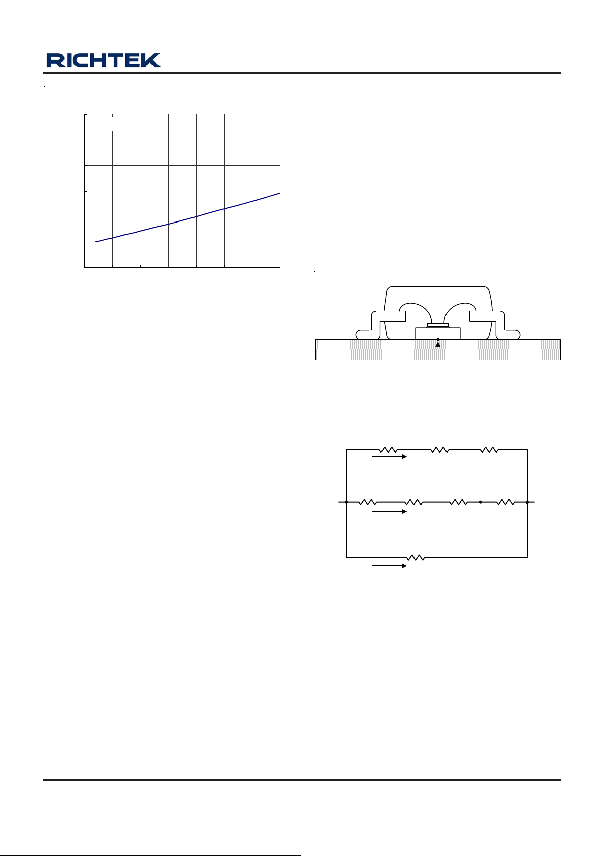
Figure 6 show the package sectional drawing of SOP-8
(Exposed Pad). Every package has several thermal
dissipation paths. As show in Figure 7, the thermal
resistance equivalent circuit of SOP-8 (Exposed Pad). The
path 2 is the main path due to these materials thermal
conductivity. We define the exposed pad is the case point
of the path 2.
Ambient
Molding Compound
Case (Exposed Pad)
Die Pad
Gold Line
Lead Frame
Figure 6. SOP-8 (Exposed Pad) Package Sectional
Drawing
Junction
R
GOLD-LINERLEAD FRAME
path 1
R
DIERDIE-ATTACHRDIE-PAD
path 2
R
MOLDING-COMPOUND
R
PCB
R
PCB
Case
(Exposed Pad)
Ambient
PD = (V
The maximum power dissipation depends on the thermal
resistance of IC package, PCB layout, the rate of
surroundings airflow and temperature difference between
junction to ambient. The maximum power dissipation can
be calculated by following formula:
P
D(MAX)
Where T
temperature 125°C, TA is the ambient temperature and the
θJA is the junction to ambient thermal resistance. The
junction to ambient thermal resistance (θJA is layout
dependent) for SOP-8 package (Exposed Pad) is 75°C/W
DS9173C-13 April 2011 www.richtek.com
- V
IN
= ( T
J(MAX)
OUT
J(MAX)
) x I
OUT
-TA ) /θ
+ VIN x I
JA
Q
is the maximum operation junction
Figure 7. Thermal Resistance Equivalent Circuit
The thermal resistance θJA of SOP-8 (Exposed Pad) is
determined by the package design and the PCB design.
However, the package design has been decided. If possible,
it's useful to increase thermal performance by the PCB
design. The thermal resistance can be decreased by
adding copper under the expose pad of SOP-8 package.
About PCB layout, the Figure 8 show the relation between
thermal resistance θJA and copper area on a standard
JEDEC 51-7 (4 layers, 2S2P) thermal test board at
TA = 25°C.We have to consider the copper couldn't stretch
path 3
11
Page 12

RT9173C
infinitely and avoid the tin overflow. We use the “dog-bone”
copper patterns on the top layer as Figure 9.
As shown in Figure 10, the amount of copper area to which
the SOP-8 (Exposed Pad) is mounted affects thermal
performance. When mounted to the standard SOP-8
(Exposed Pad) pad of 2 oz. copper (Figure 10.a), θJA is
75°C/W. Adding copper area of pad under the SOP-8
(Exposed Pad) (Figure 10.b) reduces the θJA to 64°C/W.
Even further, increasing the copper area of pad to 70mm
(Figure 10.e) reduces the θJA to 49°C/W.
θJA vs. Copper Area
100
Figure 10 (a). Minimum Footprint, θ
2
= 75°C/W
JA
90
80
70
(°C/W)
60
JA
θ
50
40
30
0 10 203040506070
Copper Area (mm2)
Figure 8
Exposed Pad
Figure 10 (b). Copper Area = 10mm2, θ
Figure 10 (c). Copper Area = 30mm2, θ
Figure 10 (d). Copper Area = 50mm2, θ
= 64°C/W
JA
= 54°C/W
JA
= 51°C/W
JA
12
W≦2.28mm
Figure 9.Dog-Bone layout
Figure 10 (e). Copper Area = 70mm2, θJA = 49°C/W
Figure 10. Thermal Resistance vs. Different Cooper Area
Layout Design
DS9173C-13 April 2011www.richtek.com
Page 13

Outline Information
RT9173C
H
M
EXPOSED THERMAL PAD
(Bottom of Package)
A
Y
J
I
B
X
F
C
D
Dimensions In Millimeters Dimensions In Inches
Symbol
Min Max Min Max
A 4.801 5.004 0.189 0.197
B 3.810 4.000 0.150 0.157
C 1.346 1.753 0.053 0.069
D 0.330 0.510 0.013 0.020
F 1.194 1.346 0.047 0.053
H 0.170 0.254 0.007 0.010
I 0.000 0.152 0.000 0.006
J 5.791 6.200 0.228 0.244
M 0.406 1.270 0.016 0.050
X 2.000 2.300 0.079 0.091
Option 1
Y 2.000 2.300 0.079 0.091
X 2.100 2.500 0.083 0.098
Option 2
Y 3.000 3.500 0.118 0.138
8-Lead SOP (Exposed Pad) Plastic Package
Richtek Technology Corporation
Headquarter
5F, No. 20, Taiyuen Street, Chupei City
Hsinchu, Taiwan, R.O.C.
Tel: (8863)5526789 Fax: (8863)5526611
Richtek Technology Corporation
Taipei Office (Marketing)
5F, No. 95, Minchiuan Road, Hsintien City
Taipei County, Taiwan, R.O.C.
Tel: (8862)86672399 Fax: (8862)86672377
Email: marketing@richtek.com
Information that is provided by Richtek Technology Corporation is believed to be accurate and reliable. Richtek reserves the right to make any change in circuit design,
specification or other related things if necessary without notice at any time. No third party intellectual property infringement of the applications should be guaranteed
by users when integrating Richtek products into any application. No legal responsibility for any said applications is assumed by Richtek.
DS9173C-13 April 2011 www.richtek.com
13
Page 14

 Loading...