

RT9173/A
DS9173/A-06 March 2002 www.richtek-ic.com.tw
1
1.5A/3A Bus Termination Regulator
General Description
The RT9173/A regulator is designed to convert
voltage supplies ranging from 1.8V to 6V into a
desired output voltage which adjusted by two external
resistors, voltage divider. The regulator is capable of
sourcing or sinking up to 1.5A/3A of current while
regulating an output voltage to within 2% or less.
The RT9173/A, used in conjunction with series
termination resistors, provides an excellent voltage
source for active termination schemes of high speed
transmission lines as those seen in high speed
memory buses and distributed backplane designs.
The voltage output of the regulator can be used as a
termination voltage for DDR SDRAM.
Current limits in both sourcing and sinking mode, plus
on-chip thermal shutdown make the circuit tolerant of
the output fault conditions.
Applications
z
Computers
z
Disk Drives
z
CD-ROM
z
Supply Splitter
z
Graph Card
Ordering Information
RT9173/A
Features
z
Support Both DDR 1 (1.25VTT) and DDR 2
(0.9VTT) Requirements
z
Power TO-263-5 and SOP-8 Packages
z
Capable of Sourcing and Sinking Current
1.5A/3A
z
Current-limiting Protection
z
Thermal Protection
z
Integrated Power MOSFETs
z
Generates Termination Voltages for SSTL-2
z
High Accuracy Output Voltage at Full-load
z
Adjustable VOUT by External Resistors
z
Minimum External Components
z
Shutdown for Standby or Suspend Mode
Operation with High-impedance Output
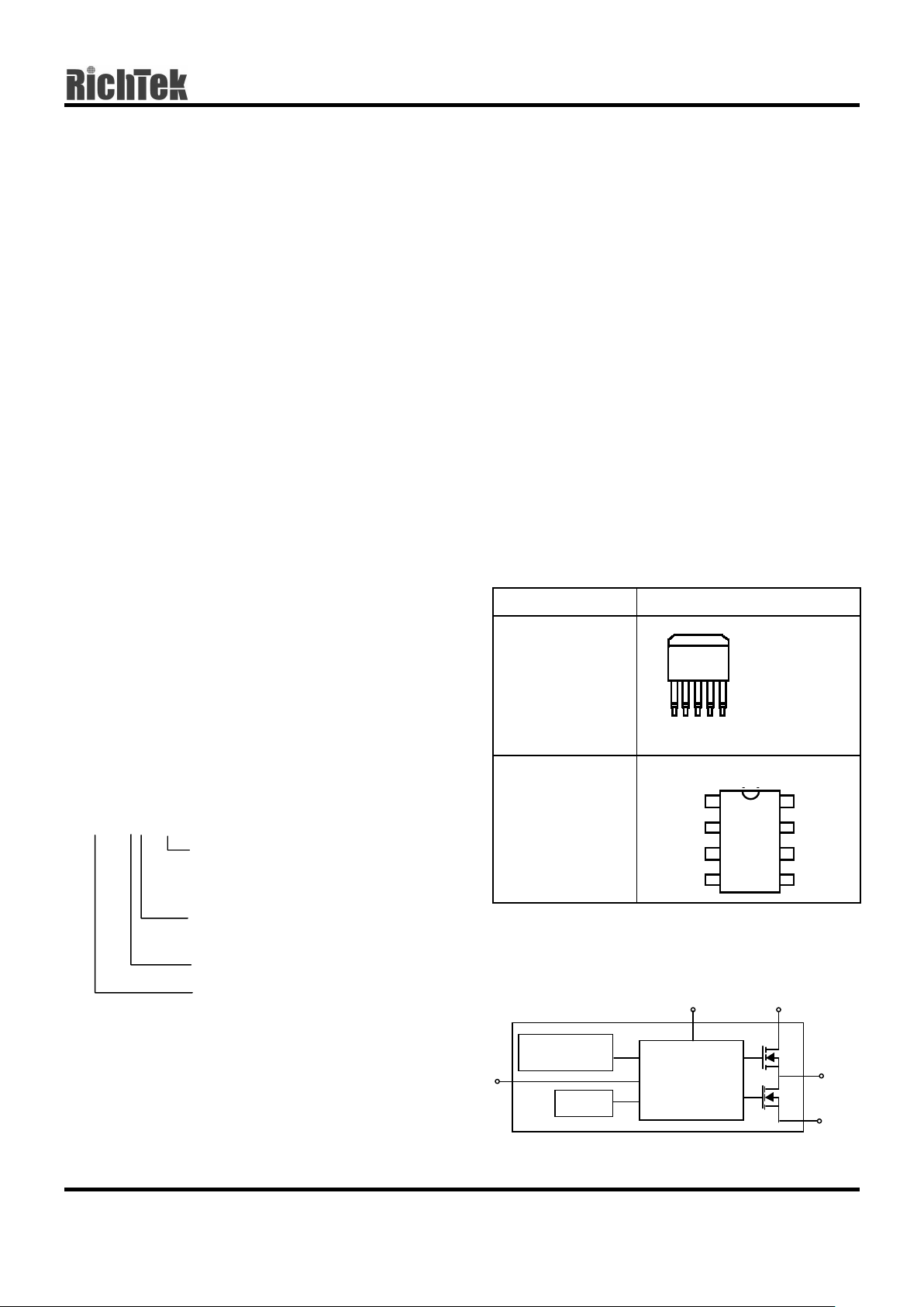
Pin Configurations
Part Number Pin Configurations
RT9173ACM5
(Plastic TO-263-5)
TOP VIEW
1. VIN
2. GND
3. VCNTL (TAB)
4. REFEN
5. VOUT
RT9173CS
(Plastic SOP-8)
TOP VIEW
Function Block Diagram
Operating temperature range
C: Commercial standard
Package type
M5 : TO-263-5
S : SOP-8
3A sink & source
1.5A sink & source
Thermal
Current
Limit ing S en sor
VOUT
REFE N
GND
CNTL
VINVCNTL
12 34 5
VIN
GND
REFE N
VOUT
1
2
3
4
8
7
6
5
VCNTL
VCNTL
VCNTL
VCNTL
RT9173/A
www.richtek-ic.com.tw DS9173/A-06 March 2002
2
Pin Description
Pin Name Pin Function
VIN Power Input
GND Ground
VCNTL Gate Drive Voltage
REFEN Reference Voltage Input and Chip Enable
VOUT Output Voltage
Absolute Maximum Ratings
z
Input Voltage 7V
z
Power Dissipation Internally Limited
z
ESD Rating 2KV
z
Storage Temperature Range -65°C to 150°C
z
Lead Temperature (Soldering, 5 sec.) 260°C
z
Package Thermal Resistance
TO-263,θ
JC
7.7°C/W
TO-263,θ
JA
19.4°C/W
SOP-8, θ
JC
15.7°C/W
SOP-8, θ
JA
Note
45°C/W
Note: θ
JA
is measured with the component mounted on an evaluation PC board in free air that the required area of
copper is 300mm
2
or larger.
Electrical Characteristics
(Limits in standard typeface are for TA = 25°C, unless otherwise specified:
V
IN
= 2.5V, V
CNTL
= 3.3V, V
REFEN
= 1.25V, C
OUT
= 10µF (Ceramic))
Parameter Symbol Test Conditions Min Typ Max Units
Output Offset Voltage V
OS
Fig.1 -20 0 20 mV
IL : 0 → 1.5A, Fig.1 -- 0.8 2
Load Regulation ∆V
LOAD
IL : 0A → -1.5A -- 0.8 2
%
V
IN
1.8 2.5 --
Input Voltage Range
(DDR 1)
V
CNTL
Keep V
CNTL
≥ VIN on operation
power on and power off sequences
-- 3.3 6
V
Current In Shutdown Mode I
SHDN
V
REFEN
< 0.2V, RL = 180Ω, Fig.2 -- 50 90 µA
Short Circuit Protection
RT9173 Fig.3,4 2.1 -- --
Current limit
RT9173A
I
LIMIT
Fig.3,4 3.0 -- --
A
Over Temperature Protection
Thermal Shutdown Temperature T
SD
3.3V ≤ V
CNTL
≤ 5V 125 150 -- °C
Thermal Shutdown Hysteresis Guaranteed by design -- 50 -- °C
Shutdown Function
Output = High, Fig.5 0.8 -- --
Shutdown Threshold Trigger
Output = Low, Fig.5 -- -- 0.2
V
RT9173/A
DS9173/A-06 March 2002 www.richtek-ic.com.tw
3
Typical Application Circuit
Test Circuit
Fig.1 Output Voltage Tolerance, ∆V
OUT
Fig.2 Current in Shutdown Mode, I
SHCLN
R1 = R
2
= 100KΩ, RTT = 50Ω / 33Ω / 25Ω
C
OUT,min
= 10µF (Ceramic) + 1000µF under the worst case testing condition
R
DUMMY
= 1kΩ as for VOUT discharge when VIN is not present but VCNTL is present
C
SS
= 1µF, CIN = 470µF (Low ESR), C
CNTL
= 47µF
VIN VCNTL
REFEN VOUT
GND
R
TT
V
CNTL
= 3.3V
V
IN
= 2.5V
EN
R
2
C
SS
R
1
C
IN
C
OUT
C
CNTL
RT9173/A
R
DUMMY
2N70 02
VIN VCNTL
REFE N
RT9173/A
VOUT
GND
1. 25 V
2. 5V 3. 3V
V
OU T
C
OUT
I
L
V
VIN VCNTL
REFE N
RT9173/A
VOUT
GND
1.25V
2.5V
3.3V
V
OU T
C
OUT
V
R
L
A
0.2V
0V
1.25V
RL and C
OUT
Time d elay

RT9173/A
www.richtek-ic.com.tw DS9173/A-06 March 2002
4
Fig.3 Current Limit for High Side, I
CLHIGH
Fig.4 Current Limit for Low Side, I
CLLOW
Fig.5 REFEN Pin Shutdown Threshold, V
TRIGGER
VIN VCNTL
REFE N
RT91 73/A
VOUT
GND
1. 25 V
2. 5V
3. 3V
V
OU T
C
OUT
I
L
VA
Power supply
with current limit
VIN VCNTL
REFE N
RT9173/A
VOUT
GND
1.25V
2.5V
3.3V
V
OUT
C
OUT
V
A
I
L
VIN VCNTL
REFE N
RT9173/A
VOUT
GND
2. 5V
3. 3V
V
OU T
C
OUT
V
R
L
0. 2V
0V
1. 25 V
1. 25 V
V
OU T
V
REFEN
RL and C
OUT
Time d elay
V
OU T
woul d be low if VREFEN < 0 .2V
V
OU T
would be hi gh if VREFEN > 0.8V

RT9173/A
DS9173/A-06 March 2002 www.richtek-ic.com.tw
5
Typical Operating Characteristics
Time (250µS/Div)
Output Transient
Voltage (mV)
Transient Response
100
50
0
-50
Output Current (A)
2
1
0
-1
-2
≈
≈
VIN = 2.5V V
CNTL
= 3.3V
V
REFEN
= 1.25V Swing Frequency = 1KHz
Time (5mS/Div)
12
10
8
6
Output Short Circuit (A)
4
2
0
-2
-4
VIN = 2.5V
V
CNTL
= 3.3V
V
REFEN
= 1.25V
Force the output shorted to ground
Sourcing Current (Peak) vs. Temp.
0.0
1.0
2.0
3.0
4.0
5.0
6.0
7.0
8.0
-40-200 20406080100120
Temperature ( C)
Sourcing Current (A)
°
V
CNTL
= 3.3V
VIN = 2.5V
V
OUT
= 1.25V
Sinking Current (Peak) vs. Temp.
0.0
1.0
2.0
3.0
4.0
5.0
6.0
7.0
8.0
-40 -20 0 20 40 60 80 100 120
Temperature ( C)
Sinking Current (A)
°
V
CNTL
= 3.3V
V
IN
= 2.5V
V
OUT
= 1.25V
Turn-On Threshold vs. Temp.
400
450
500
550
600
650
700
-40 -20 0 20 40 60 80 100 120
Temperature ( C)
Threshold Voltage (mV)
°
V
CNTL
= 3.3V
VIN = 2.5V
Turn-On Threshold vs. Temp.
400
450
500
550
600
650
700
-40 -20 0 20 40 60 80 100 120
Temperature ( C)
Threshold Voltage (mV)
°
V
CNTL
= 5.0V
VIN = 2.5V

RT9173/A
www.richtek-ic.com.tw DS9173/A-06 March 2002
6
Applications Information
Internal parasitic diode
Avoid forward-bias internal parasitic diode, VOUT to
VCNTL, and VOUT to VIN, the VOUT should not be
forced some voltage respect to ground on this pin
while the VCNTL or VIN is disappeared.
Consideration while designs the resistance of
voltage divider
Make sure the sinking current capability of pull-down
NMOS if the lower resistance was chosen so that the
voltage on REFEN is below 0.2V.
In addition to item 1, the capacitor and voltage divider
form the low-pass filter. There are two reasons doing
this design; one is for output voltage soft-start while
another is for noise immunity.
How to reduce power dissipation on Notebook PC
or the dual channel DDR SDRAM application?
In notebook application, using RichTek’s Patent
“Distributed Bus Terminator Topology” with choosing
RichTek’s product is encouraged.
Thermal Consideration
RT9173/A regulators have internal thermal limiting
circuitry designed to protect the device during
overload conditions. For continuous normal load
conditions however, the maximum junction
temperature rating of 125°C must not be exceeded.
Higher continous currents or ambient temperature
require additional heatsinking. Heat sinking to the IC
package must consider the worst case power
dissipation which may occur.
It should also be note that with the VCNTL equal to
5V, the point of thermal shutdown will be degraded by
approx. 20°C compared to the VCNTL equipped with
3.3V. It is highly recommended that to use the 3.3V
rail acted as the VCNTL so as to minimize the
thermal concern of the RT9173CS in the SOP-8
package.
Layout Consideration
The RT9173CS regulator is packaged in plastic SOP-
8 package. This small footprint package is unable to
convectively dissipate the heat generated when the
regulator is operating at high current levels. In order
to control die operating temperatures, the PC board
layout should allow for maximum possible copper
area at the VCNTL pins of the RT9173CS.
The multiple VCNTL pins on the SOP-8 package are
internally connected, but lowest thermal resistance
will result if these pins are tightly connected on the
PC board. This will also aid heat dissipation at high
power levels.
If the large copper around the IC is unavailable, a
buried layer may be used as a heat spreader, Use
vias to conduct the heat into the buried or backside of
PCB layer. The vias should be small enough to retain
solder when the board is wave-soldered. (See Fig.6
shown on next page).
Distributed Bus Terminating Topology
R0
R2
R3
R4
R5
R6
R7
R8
R9
RN
BUS(0)
BUS(1)
BUS(2)
BUS(3)
BUS(4)
R1
BUS(5)
BUS(6)
BUS(7)
BUS(8)
BUS(9)
BUS(N+1)
RN1
BUS(N)
Terminator Resistor
RT9173
RT9173
VOUT
VOUT
REFE N

RT9173/A
DS9173/A-06 March 2002 www.richtek-ic.com.tw
7
Fig. 6 Layout Consideration
To prevent this maximum junction temperature from
being exceeded, the appropriate power plane heat
sink MUST be used. Higher continuous currents or
ambient temperature require additional heatsinking.
RT9173CS (SOP-8)
The PCB heat sink copper area should be
solder-painted without masked. This
approaches a “best case” pad heat sink.
Use vias to conduct the heat into the
buried or backside of PCB layer .
RT9173CS (SOP-8)
The PCB heat sink copper area should be
solder-painted without masked. This
approaches a “best case” pad heat sink.
Use vias to conduct the heat into the
buried or backside of PCB layer .

RT9173/A
www.richtek-ic.com.tw DS9173/A-06 March 2002
8
Package Information
Dimensions In Millimeters Dimensions In Inches
Symbol
Min Max Min Max
D 9.652 10.668 0.380 0.420
B 1.143 1.676 0.045 0.066
E 8.128 9.652 0.320 0.380
A 4.064 4.826 0.160 0.190
C 1.143 1.397 0.045 0.055
U 6.223 Ref. 0.245 Ref.
V 7.620 Ref. 0.300 Ref.
L1 14.605 15.875 0.575 0.625
L2 2.286 2.794 0.090 0.110
b 0.660 0.914 0.026 0.036
b2 0.305 0.584 0.012 0.023
e 1.524 1.829 0.060 0.072
5-Lead TO-263 Plastic Surface Mount Package
e
MARK
b
L1
D
E
B
L2
C
A
b2
V
U

RT9173/A
DS9173/A-06 March 2002 www.richtek-ic.com.tw
9
Dimensions In Millimeters Dimensions In Inches
Symbol
Min Max Min Max
A 4.801 5.004 0.189 0.197
B 3.810 3.988 0.150 0.157
C 1.346 1.753 0.053 0.069
D 0.330 0.508 0.013 0.020
M 0.406 1.270 0.016 0.050
F 1.194 1.346 0.047 0.053
I 0.102 0.254 0.004 0.010
J 5.791 6.198 0.228 0.244
H 0.178 0.254 0.007 0.010
8–Lead SOP Plastic Package
F
A
J
B
D
I
C
M
H

RT9173/A
www.richtek-ic.com.tw DS9173/A-06 March 2002
10
RICHTEK TECHNOLOGY CORP.
Headquarter
6F, No. 35, Hsintai Road, Chupei City
Hsinchu, Taiwan, R.O.C.
Tel: (8863)5510047 Fax: (8863)5537749
RICHTEK TECHNOLOGY CORP.
Taipei Office (Marketing)
8F-1, No. 137, Lane 235, Paochiao Road, Hsintien City
Taipei County, Taiwan, R.O.C.
Tel: (8862)89191466 Fax: (8862)89191465
Email: marketing@richtek-ic.com.tw
 Loading...