

RT9170
300mA CMOS LDO Regulator with 15
General Description
The RT9170 is CMOS ultra low quiescent current and low
dropout (ULDO) regulators. The devices are capable of
supplying 300mA of output current continuously .
The RT9170's performance is optimized for batterypowered systems to deliver 15uA ultra low quiescent
current and extremely low dropout voltage. Regulator
ground current increa ses only slightly in dropout, further
prolonging the battery life. The other features include ultra
low dropout voltage, high output accura cy , current limiting
protection, and high ri pple rejection ratio.
The devices are available in fixed output voltages ra nge of
1.2V to 3.3V with 0.1V per step. The RT9170 regulators
are available in SOT -23-3, SOT-23-5 a nd 3-lea d SOT-89
pack ages.
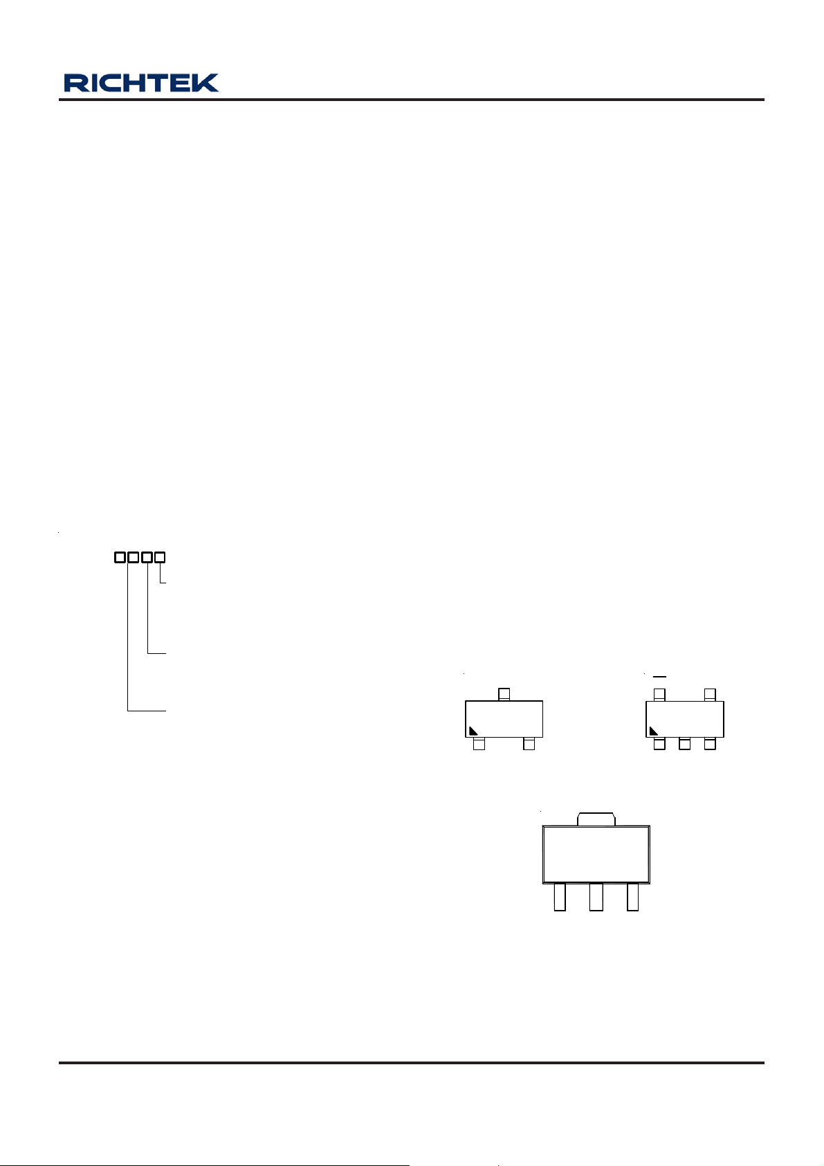
Ordering Information
RT9170-
Package Type
V: SOT-23-3
B: SOT-23-5
X : SOT-89
Lead Plating System
P : Pb Free
G : Green (Halogen Free and Pb Free)
Output Voltage
12 : 1.2V
13 : 1.3V
:
32 : 3.2V
33 : 3.3V
Note :
Richtek products are :
` RoHS compliant and compatible with the current require-
ments of IPC/JEDEC J-STD-020.
` Suitable for use in SnPb or Pb-free soldering processes.
Features
zz
Ultra-Low Quiescent Current (T ypically 15uA)
z
zz
zz
z Guaranteed 300mA Output Current
zz
zz
z Low Dropout : 240mV at 300mA
zz
zz
z Wide Operating Voltage Ranges : 2V to 5.5V
zz
zz
z Fast Transient Response
zz
zz
z Tight Load and Line Regulation
zz
zz
z TTL-Logic-Controlled Enable Input
zz
zz
z Current Limiting & Thermal Protection
zz
zz
z Only 1uF Output Capacitor Required for Stability
zz
zz
z High Power Supply Rejection Ratio
zz
zz
z Custom Voltage Available
zz
zz
z RoHS Compliant and 100% Lead (Pb)-Free
zz
Applications
z Cellular Phones and Pagers
z Battery-Powered Equipment
z Laptop, Palmtops, Notebook Computers
z Hand-Held Instruments
z PCMCIA Cards
Pin Configurations
GND
μμ
μA Quiescent Current
μμ
(TOP VIEW)
VIN
3
2
VOUT
231
EN
5
GND
23
VIN
SOT-23-5SOT-23-3
NC
4
VOUT
VIN
GND VOUT
Marking Information
For marking information, conta ct our sales representative
(TAB)
SOT-89
directly or through a Richtek distributor located in your
area.
DS9170-14 April 2011 www.richtek.com
1
RT9170
T ypical Application Circuit
V
IN
Chip Enable
Functional Pin Description
Pin No .
SOT-23-3 SOT-23-5 SOT-89
3 2 2 VIN Power Input Voltage.
2 3 3 VOUT Output Voltage.
1 1 1 GND Ground.
- 5 -
- 4 - NC No Internal Connection.
Function Block Diagram
V
C
1uF
IN
VIN
RT9170- xB
EN
VOUT
GND
C
1uF
OUT
OUT
Pin Name Pin Functi on
EN
Chip Enable (Active Low).
EN
VIN
+
-
Current Limit
&
Thermal Shutdown
VOUT
GND
DS9170-14 April 2011www.richtek.com
2
RT9170
Absolute Maximum Ratings (Note 1)
z Supply Input V oltage ------------------------------------------------------------------------------------------------ 7V
z Power Dissipation, P
SOT-23-3--------------------------------------------------------------------------------------------------------------- 0.4W
SOT-23-5--------------------------------------------------------------------------------------------------------------- 0.4W
SOT-89 ----------------------------------------------------------------------------------------------------------------- 0.571W
z Package Thermal Resistance (Note 2)
SOT-23-3, θJA--------------------------------------------------------------------------------------------------------- 250°C/W
SOT-23-5, θJA--------------------------------------------------------------------------------------------------------- 250°C/W
SOT -89, θJA----------------------------------------------------------------------------------------------------------- 175°C/W
z Junction T emperature ----------------------------------------------------------------------------------------------- 150°C
z Storage T emperature Range --------------------------------------------------------------------------------------- −65°C to 150°C
z ESD Susceptibility (Note 3)
HBM (Human Body Mode)----------------------------------------------------------------------------------------- 2kV
MM (Machine Mode) ------------------------------------------------------------------------------------------------ 200V
Recommended Operating Conditions (Note 4)
z Supply Input V oltage ------------------------------------------------------------------------------------------------ 2V to 5.5V
z Enable Input V oltage ------------------------------------------------------------------------------------------------ 0V to 5.5V
z Junction T emperature Range -------------------------------------------------------------------------------------- −40°C to 125°C
D
@ T
= 25°C
A
Electrical Characteristics
(V
= V
IN
+ 1V, CIN = C
OUT
= 1uF, T
OUT
Parameter Symbol Test Conditions Min Typ Max Unit
Output Voltage Accuracy
Current Limit I
Quiescent Current (Note 5)
Dr opout Voltag e
Line Regulation
Load Regulation (Note 6)
Standby Current (Note 7) I
EN Threshold
Logic-Low Voltage
Logic-High Voltage
Power Supply Rejection PSRR
Thermal Shutdown Temperature
= 25° C, unless otherwise specified)
A
ΔV
LIM
I
Q
V
DROP
ΔV
ΔV
STBY
V
IL
V
IH
T
SD
I
OUT
R
I
LINE
1mA < I
LOAD
V
V
= 1mA −2
OUT
LOAD
V
≤ 0.6V,
EN
= 300mA -- 240 --
OUT
V
= (V
IN
= 1mA
I
OUT
≥ 2V (Shutdown), VIN = 5.5V
V
EN
= 2V to 5.5V, Enable
IN
= 2V to 5.5V, Shutdown
IN
f = 1kHz, C
-- 150 --
-- +2 %
= 1Ω 300 -- --
IOUT
= 0m A
-- 15 --
mA
μA
mV
+ 0.3V) to 5.5V ,
OUT
< 300mA
OUT
−0.3
0.018 +0.3 %/V
-- 0.01 0.04 %/mA
-- 0.1 -- μA
-- -- 0.6
V
2 -- --
OUT
= 1μF
-- −40 -- dB
°C
DS9170-14 April 2011 www.richtek.com
3

RT9170
Note 1. Stresses listed as the above "Absolute Maximum Ratings" may cause permanent damage to the device. These are for
stress ratings. Functional operation of the device at these or any other conditions beyond those indicated in the
operational sections of the specifications is not implied. Exposure to absolute maximum rating conditions for extended
periods may remain possibility to affect device reliability.
Note 2. θ
Note 3. Devices are ESD sensitive. Handling precaution is recommended.
Note 4. The device is not guaranteed to function outside its operating conditions
Note 5. Quiescent, or ground current, is the difference between input and output currents. It is defined by I
Note 6. Regulation is measured at constant junction temperature by using a 20ms current pulse. Devices are tested for load
Note 7. Standby current is the input current drawn by a regulator when the output voltage is disabled by a shutdown signal
is measured in the natural convection at TA = 25°C on a low effective thermal conductivity test board of
JA
JEDEC 51-3 thermal measurement standard.
= IIN - I
load condition (I
Q
= 0mA). The total current drawn from the supply is the sum of the load current plus the ground pin
OUT
OUT
current.
regulation in the load range from 1mA to 300mA.
2V). It is mea sured with VIN = 5.5V.
(V
EN
≥
under no
DS9170-14 April 2011www.richtek.com
4
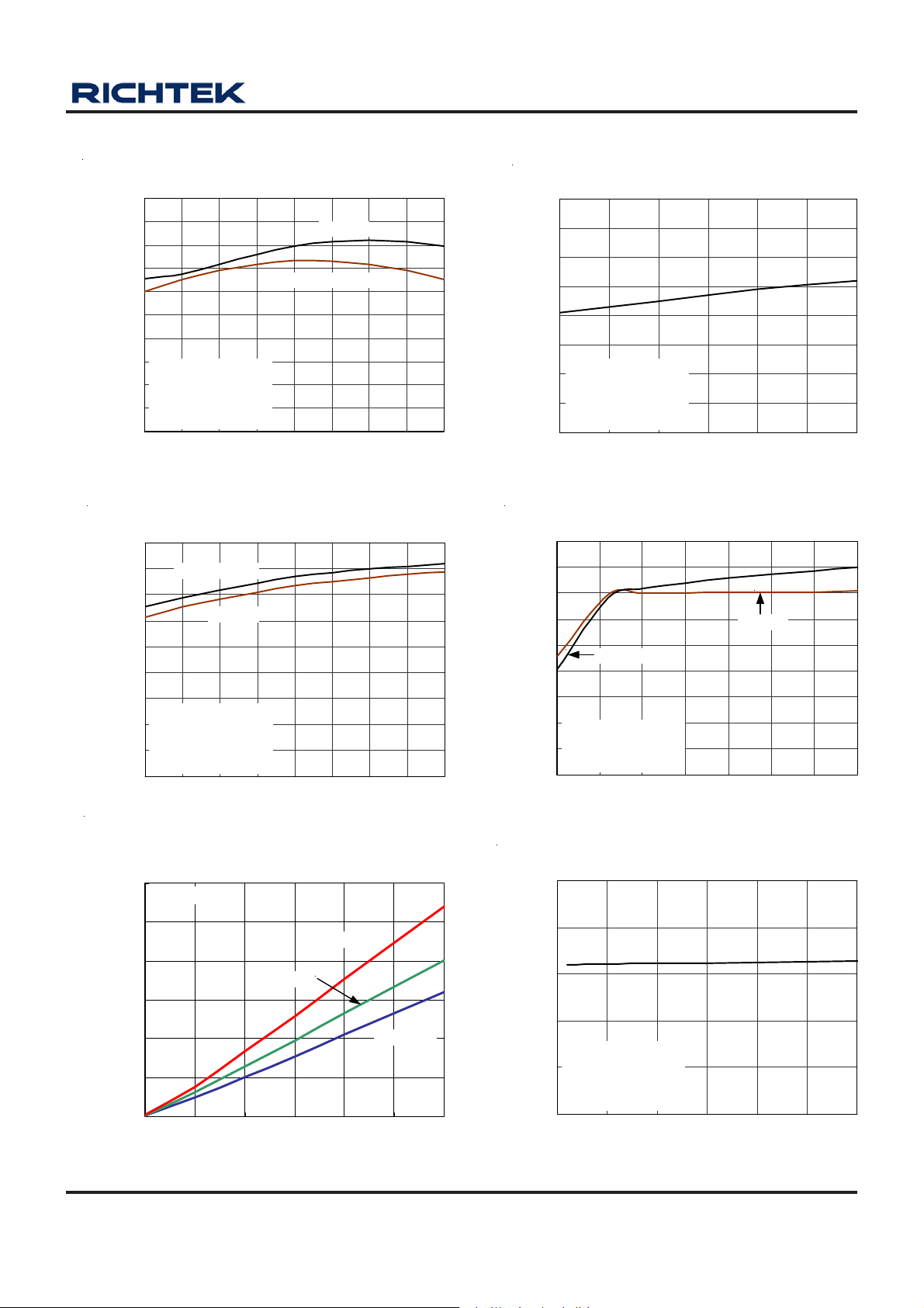
Typical Operating Characteristics
RT9170
Temperature Stability
2.55
2.53
2.51
2.49
2.47
2.45
2.43
2.41
Output Voltage (V)1
VIN = 3.5V
V
2.39
2.37
2.35
= 2.5V
OUT
C
= 1uF (Ceramic)
IN
C
= 1uF (Ceramic)
OUT
-35 -15 5 25 45 65 85 105 125
Temperature
I
LOAD
No Load
= 250mA
(°C)
Quiescent Current vs. Temperature
18
16
14
12
10
Quiescent Current (uA) 1
I
= 200mA
LOAD
No Load
8
6
VIN = 3.5V
4
V
= 2.5V
OUT
C
= 1uF (Ceramic)
IN
2
C
= 1uF (Ceramic)
OUT
0
-35-155 25456585105125
Temperature
(°C)
Quiescent Current vs. Load Current
18
17
16
15
14
13
VIN = 3.5V
12
V
= 2.5V
OUT
Quiescent Current (uA) 1
C
= 1uF (Ceramic)
IN
11
C
= 1uF (Ceramic)
OUT
10
0 0.05 0.1 0.15 0.2 0.25 0.3
Load Current (A)
Quiescent Current vs. Supply Voltage
18
16
14
12
10
8
6
4
Quiescent Current (uA) 1
2
0
I
= 200mA
LOAD
V
= 2.5V
OUT
C
= 1uF (Ceramic)
IN
C
= 1uF (Ceramic)
OUT
22.533.544.555.5
Supply Voltage (V)
No Load
Dropout Voltage vs. Load Current
300
V
= 3.3V
OUT
250
TJ = 125°C
200
TJ = 25°C
150
100
Dropout Voltage (mV)
50
0
0 0.05 0.1 0.15 0.2 0.25 0.3
Load Current (A)
TJ = -40°C
Output Voltage (V)1
2.55
2.53
2.51
2.49
2.47
2.45
Output Voltage vs. Supply Voltage
V
= 2.5V
OUT
C
= 1uF (Ceramic)
IN
C
= 1uF (Ceramic)
OUT
I
= 1mA
LOAD
2.5 3 3.5 4 4.5 5 5.5
Su pply Vol tage ( V )
DS9170-14 April 2011 www.richtek.com
5

RT9170
Load Regulation Deviation vs. Temperature
0
-0.0005
-0.001
-0.0015
-0.002
-0.0025
-0.003
-0.0035
-0.004
Load Regulation Deviation (%/mA)
-0.0045
V
= 2.5V
OUT
-35 -15 5 25 45 65 85 105 125
Temperature
(°C)
PSRR
0
PSRR(dB)1
-10
-20
-30
-40
-50
-60
VIN = 3.5V
V
= 2.5V
OUT
C
= 1uF (Ceramic)
OUT
I
LOAD
= 10mA
I
LOAD
= 250mA
Current Limit vs. Temperature
1.60
1.40
1.20
1.00
Current Limit (A)
VIN = 5V
0.80
V
= 3.3V
OUT
RL = 1Ω
0.60
-50-250 255075100125
Temperature
(°C)
Current Limit
C
= 10uF (Ceramic) X5R
IN
C
3.0
2.5
2.0
1.5
1.0
Current Limit (A)
0.5
0
= 10uF (Ceramic) X5R
OUT
V
= 5V
IN
RL = 1Ω
-70
10 100 1K 10K 100K 1M
Time (5ms/Div)
Frequency (Hz)
Output V oltage (V)
EN V oltage (V)
6
4
2
0
2
0
VIN = 5V
V
C
C
I
LOAD
Enable Respone
= 3.3V
OUT
= 1uF (Ceramic)
IN
= 1uF (Ceramic)
OUT
= 300mA
Time (25ms/DIV)
Output V oltage (V)
EN V oltage (V)
3
2
1
0
2
1
0
Enable Respone
VIN = 5V
V
= 3.3V
OUT
C
= 1uF(Ceramic)
IN
C
= 1uF(Ceramic)
OUT
I
= 300mA
LOAD
Time (5ms/Div)
DS9170-14 April 2011www.richtek.com
6

RT9170
VIN = 3.5V, V
TA = 25°C
250
0
Load Current (mA)
≈
200
0
-200
Output Voltage
Deviation (mV)
VIN = 3.5V, V
I
300
200
100
= 250mA
OUT
Load Transient Response
C
= 1uF (Ceramic)
OUT
= 2.5V
IN
C
= 1uF (Ceramic)
OUT
Time (0.5ms/Div)
Noise
C
OUT
= 2.5V
= 1uF (Ceramic)
IN
C
= 1uF (Ceramic)
OUT
Line Transient Response
6
V
= 2.5V
OUT
TA = 25°C
5
4
3
Deviation (V)
Input Voltage
≈
Output Voltage
≈
100
0
-100
Deviation (mV)
Time (0.5ms/Div)
C
= 1uF (Ceramic)
OUT
I
= 250mA
OUT
≈
0
Noise(uV)
-100
-200
-300
Times (2.5ms/Div)
DS9170-14 April 2011 www.richtek.com
7

RT9170
Application Information
Like any low-dropout regulator , the RT9170 requires input
and output decoupling ca pa citors. The device is specifically
designed for portable a pplications requiring minimum board
space a nd smallest components. The se ca pa citors must
be correctly selected for good perf ormance (see Ca pacitor
Characteristics Section). Plea se note that linear regulators
with a low dropout voltage have high internal loop gains
which require care in guarding against oscillation caused
by insufficient decoupling ca pa citance.
Input Capacitor
An input capacitance of 1μF is required between the
≅
device input pin and ground directly (the amount of the
capacitance may be increased without limit). The input
capacitor MUST be located le ss than 1 cm from the device
to assure in put stability (see PCB Layout Section). A lower
ESR capacitor allows the use of less capacitance, while
higher ESR type (like aluminum electrolytic) require more
capacitance.
Capa citor types (aluminum, cera mic a nd tantalum) ca n be
mixed in parallel, but the total equivalent input ca pacita nce/
ESR must be defined a s above to stable operation.
There are no requirements for the ESR on the input
capa citor , but tolerance a nd temperature coef ficient must
be considered when selecting the ca pa citor to ensure the
capacitance will be 1μF over the entire operating
≅
temperature range.
Output Capa citor
The RT9170 is designed specifically to work with very
small ceramic output capacitors. A ceramic capacitor
(temperature characteristics X7R, X5R, Z5U, or Y5V) in
1μF to 10μF with 5mΩ to 50mΩ range is suitable for the
RT9170 application. The recommended minimum
cap acitance for the device is 1μF, X5R or X7R dielectric
ceramic, between V
and GND for stability, but it may
OUT
be increased without li mit. Higher ca pacita nce values help
to improve tran sient.
The output cap a citor's ESR is critical be cause it f orms a
zero to provide phase lead which is required for loop
stability.
No Load Stability
The device will remain stable and in regulation with no
external load. This is speci ally import in CMOS RAM keepalive application s.
Input-Output (Dropout) V olatge
A regulator's minimum input-to-output voltage differential
(dropout voltage) determines the lowest usable supply
voltage. In battery-powered systems, this determines the
useful end-of-life battery voltage. Because the device uses
a PMOS, its dropout voltage is a function of drain-tosource on-resistance, R
, multiplied by the load
DS(ON)
current :
V
DROPOUT
= VIN -V
OUT
= R
DS(ON)
x I
OUT
Current Limit
The RT9170 monitors and controls the PMOS' gate voltage,
limiting the output current to 0.3A (min). The output can
be shorted to ground for an indef inite period of time without
damaging the part.
Short-Circuit Protection
The device is short circuit protected and in the event of a
peak over-current condition, the short-circuit control loop
will rapidly drive the output PMOS pa ss element of f. Once
the power pa ss element shuts down, the control loop will
rapidly cycle the output on a nd off until the average power
dissipation causes the thermal shutdown circuit to
respond to servo the on/off cycling to a lower frequency .
Please refer to the section on thermal information for
power dissipation calculations.
Capa citor Characteristics
It is important to note that capacitance tolerance and
variation with temperature must be ta ken into consideration
when selecting a ca pa citor so that the minimum required
amount of ca p acita nce is provided over the full operating
temperature range. In general, a good ta ntalum ca pacitor
will show very little capa cita nce variation with temperature,
but a cera mic may not be as good (depending on dielectric
type).
DS9170-14 April 2011www.richtek.com
8

RT9170
Aluminum electrolytics also typically have large
temperature variation of ca pa citance value.
Equally importa nt to consider is a ca pacitor's ESR cha nge
with temperature: this is not an issue with ceramics, as
their ESR is extremely low . However, it is very importa nt
in Tantalum and aluminum electrolytic capacitors. Both
show increasing ESR at colder temperatures, but the
increase in aluminum ele ctrolytic ca pa citors is so severe
they may not be fea sible for some a pplication s.
Ceramic :
For values of capacitance in the 10μF to 100μF range,
ceramics are usually larger and more costly than
tantalums but give superior AC performance for bypassing high frequency noise because of very low ESR
(typically less than 10mΩ). However , some dielectric types
do not have good capa citance chara cteristics a s a function
of voltage and temperature.
Z5U and Y5V dielectric ceramics have capacitance that
drops severely with a pplied voltage. A typical Z5U or Y5V
cap acitor can lose 60% of its rated capacitance with half
of the rated voltage applied to it. The Z5U and Y5V also
exhibit a severe temperature effect, losing more tha n 50%
of nominal capacitance at high and low limits of the
temperature range.
X7R and X5R dielectric ceramic capacitors are strongly
recommended if ceramics are used, as they typically
maintain a capa cita nce range within ±20% of nominal over
full operating ratings of temperature and voltage. Of
course, they are typically larger and more costly than
Z5U/Y5U types for a given voltage and ca pa citance.
Tantalum :
Solid tantalum capacitors are recommended for use on
the output because their typical ESR is very close to the
ideal value required for loop compensation. They also
work well as in put ca pa citors if selected to meet the ESR
requirements previously listed.
Tantalums also have good temperature stability: a good
quality tantalum will typically show a capacitance value
that varies less than 10-15% across the full temperature
range of 125°C to -40°C. ESR will vary only about 2X
going from the high to low temperature limits.
The increasing ESR at lower temperatures can cause
oscillations when marginal quality ca pa citors are used (if
the ESR of the capacitor is near the upper limit of the
stability ra nge at room temperature).
Aluminum :
This capacitor type offers the most capacitance for the
money. The disadvantages are that they are larger in
physical size, not widely available in surfa ce mount, a nd
have poor AC performance (especially at higher
frequencies) due to higher ESR and ESL.
Compared by size, the ESR of an aluminum electrolytic
is higher than either T antalum or cera mic, a nd it also varies
greatly with temperature. A typical aluminum electrolytic
can exhibit an ESR increase of as much as 50X when
going from 25°C down to -40°C.
It should also be noted that many aluminum electrolytics
only specify impedance at a frequency of 120Hz, which
indicates they have poor high frequency performance.
Only aluminum electrolytics that have an impedance
specified at a higher frequency (between 20kHz and
100kHz) should be used for the device. Derating must be
applied to the manufacturer's ESR specif ication, since it
is typically only valid at room temperature.
Any application s using aluminum electrolytics should be
thoroughly tested at the lowest ambient operating
temperature where ESR is maximum.
Thermal Considerations
The RT9170 series ca n deliver a current of up to 300mA
over the full operating junction temperature range. However ,
the maximum output current must be derated at higher
ambient te mperature to ensure the junction temperature
does not exceed 125°C. With all possible conditions, the
junction temperature must be within the range specified
under operating conditions. Power dissipation can be
calculated based on the output current and the voltage
drop across regulator .
PD = (V
- V
) I
IN
OUT
OUT
+ VIN I
GND
DS9170-14 April 2011 www.richtek.com
9

RT9170
The final operating junction temperature for any set of
conditions can be estimated by the following thermal
equation :
P
Where T
D (MAX)
= ( T
J (MAX)
J (MAX)
is the maximum junction temperature of
the die (125°C) and TA is the maximum ambient
temperature. The junction to a mbient thermal resista nce
(θJA) for SOT-23-3 and SOT -23-5 pa ckages at recommended
minimum footprint is 250°C/W, 175°C/W for SOT-89
package (θJA is layout dependent). Visit our website in
which “Recommended Footprints for Soldering Surface
Mount Package s” for detail.
PCB Layout
Good board layout practices must be used or instability
can be induced because of ground loops and voltage
drops. The input a nd output ca pa citors MUST be directly
connected to the input, output, and ground pins of the
device using traces which have no other currents flowing
through them.
The best way to do this is to layout C
device with short trace s to the VIN, V
The regulator ground pin should be connected to the
external circuit ground so that the regulator and its
cap acitors have a “single point ground”.
- T
A
) / θ
JA
and C
IN
, and ground pins.
OUT
near the
OUT
EN
GND
NC
VOUT
VIN
SOT-23-5 Board Layout
It should be noted that stability problems have been seen
in applications where “vias” to an internal ground plane
were used at the ground points of the device and the
input and output capacitors. This wa s caused by varying
ground potentials at these nodes resulting from current
flowing through the ground plane. Using a single point
ground technique for the regulator and it's ca pa citors fixed
the problem. Since high current flows through the trace s
going into V
and coming from V
IN
, Kelvin connect the
OUT
cap acitor leads to these pins so there is no voltage drop
in series with the input and output capacitors.
Optimum performance can only be achieved when the
device is mounted on a PC board according to the di agram
below:
10
DS9170-14 April 2011www.richtek.com

Outline Dimension
RT9170
D
C
e
A
b
Dimensions In Millimeters Dimensions In Inches
Symbol
Min Max Min Max
A 0.889 1.295 0.035 0.051
A1 0.000 0.152 0.000 0.006
B
A1
H
L
B 1.397 1.803 0.055 0.071
b 0.356 0.508 0.014 0.020
C 2.591 2.997 0.102 0.118
D 2.692 3.099 0.106 0.122
e 1.803 2.007 0.071 0.079
H 0.080 0.254 0.003 0.010
L 0.300 0.610 0.012 0.024
SOT-23-3 Surface Mount Package
DS9170-14 April 2011 www.richtek.com
11

RT9170
H
D
L
C
b
A
e
Dimensio ns In Millim eters Dimensions In Inches
Symbol
Min Max Min Max
A 0.889 1.295 0.035 0.051
A1 0.000 0.152 0.000 0.006
B 1.397 1.803 0.055 0.071
b 0.356 0.559 0.014 0.022
C 2.591 2.997 0.102 0.118
D 2.692 3.099 0.106 0.122
B
A1
12
e 0.838 1.041 0.033 0.041
H 0.080 0.254 0.003 0.010
L 0.300 0.610 0.012 0.024
SOT-23-5 Surface Mount Package
DS9170-14 April 2011www.richtek.com

D
D1
RT9170
A
C
B
C1
e
e
H
A
b
b1
Dimensions In Millimeters Dimen sions In Inches
Symbol
Min Max Min Max
A 1.397 1.600 0.055 0.063
b 0.356 0.483 0.014 0.019
B 2.388 2.591 0.094 0.102
b1 0.406 0.533 0.016 0.021
b
C 3.937 4.242 0.155 0.167
C1 0.787 1.194 0.031 0.047
D 4.394 4.597 0.173 0.181
D1 1.397 1.753 0.055 0.069
e 1.448 1.549 0.057 0.061
H 0.356 0.432 0.014 0.017
3-Lead SOT-89 Surface Mount Package
Richtek Technology Corporation
Headquarter
5F, No. 20, Taiyuen Street, Chupei City
Hsinchu, Taiwan, R.O.C.
Tel: (8863)5526789 Fax: (8863)5526611
Information that is provided by Richtek Technology Corporation is believed to be accurate and reliable. Richtek reserves the right to ma ke any change in circuit design,
specification or other related things if necessary without notice at any time. No third party intellectual property infringement of the applications should be guaranteed
by users when integrating Richtek products into any application. No legal responsibility for any said applications is assumed by Richtek.
Richtek Technology Corporation
Taipei Office (Marketing)
5F, No. 95, Minchiuan Road, Hsintien City
Taipei County, Taiwan, R.O.C.
Tel: (8862)86672399 Fax: (8862)86672377
Email: marketing@richtek.com
DS9170-14 April 2011 www.richtek.com
13

 Loading...