

Page 1

APPLICATION NOTE
SH7263/SH7203 Group
Data Transfer to On-chip Peripheral Modules with DMAC
Introduction
This application note provides an example of transferring data to on-chip peripheral modules with the direct memory
access controller (DMAC) of the SH7263/SH7203.
Target Device
SH7263/SH7203
Contents
1. Introduction ....................................................................................................................................... 2
2. Description of Sample Application.................................................................................................... 3
3. Sample Program............................................................................................................................... 9
4. Documents for Reference............................................................................................................... 15
REJ06B0734-0100/Rev.1.00 April 2008 Page 1 of 17
Page 2

SH7263/SH7203 Group
Data Transfer to On-chip Peripheral Modules with DMAC
1. Introduction
1.1 Specification
• DMAC channel 1 is used to transfer data from external memory to the transmit FIFO data register (SCFTDR) in the
serial communication interface with FIFO (SCIF channel 0) in order to transmit character string data.
• SCIF transmit FIFO data empty transfer requests (on-chip peripheral module request) are used to request DMA
transfer.
1.2 Modules Used
• Direct memory access controller (DMAC channel 1)
• Serial communication interface with FIFO (SCIF channel 0)
1.3 Applicable Conditions
• Microcontroller: SH7263/SH7203
• Operating Frequency: Internal clock 200 MHz
Bus clock 66.67 MHz
Peripheral clock 33.33 MHz
• C Compiler: SuperH RISC engine family C/C++ compiler package Ver.9.01, from Renesas
Technology
• Compile Option: -cpu = sh2afpu -fpu = single -include = "$(WORKSPDIR)\inc"
-object = "$(CONFIGDIR)\$(FILELEAF).obj" -debug -gbr = auto -chgincpath
-errorpath -global_volatile = 0 -opt_range = all -infinite_loop = 0 -del_vacant_loop = 0
-struct_alloc = 1 -nologo
1.4 Related Application Notes
• The operation of the reference program for this document was confirmed with the setting conditions described in
the application note: SH7263/SH7203 Initialization Example. Please refer to the application note in combination
with this one.
• Details on SCIF UART transmission are described in the application: SH7263/SH7203 Example Settings for UART
Transmission by the SCIF.
Please refer to the above application notes in combination with this one.
REJ06B0734-0100/Rev.1.00 April 2008 Page 2 of 17
Page 3

SH7263/SH7203 Group
Data Transfer to On-chip Peripheral Modules with DMAC
2. Description of Sample Application
In this sample application, the DMAC and on-chip peripheral module requests are used to transfer data from external
memory to the SCIF.
2.1 Operational Overview of Modules Used
When a DMA transfer request is made, the DMAC starts to transfer data in accordance with the priority order of
channels, and continues the transfer operation until the transfer end condition is met. Transfer requests for the DMAC
are of three kinds: auto requests, external requests, and on-chip peripheral module requests. The bus mode is selectable
as burst mode or cycle-stealing mode.
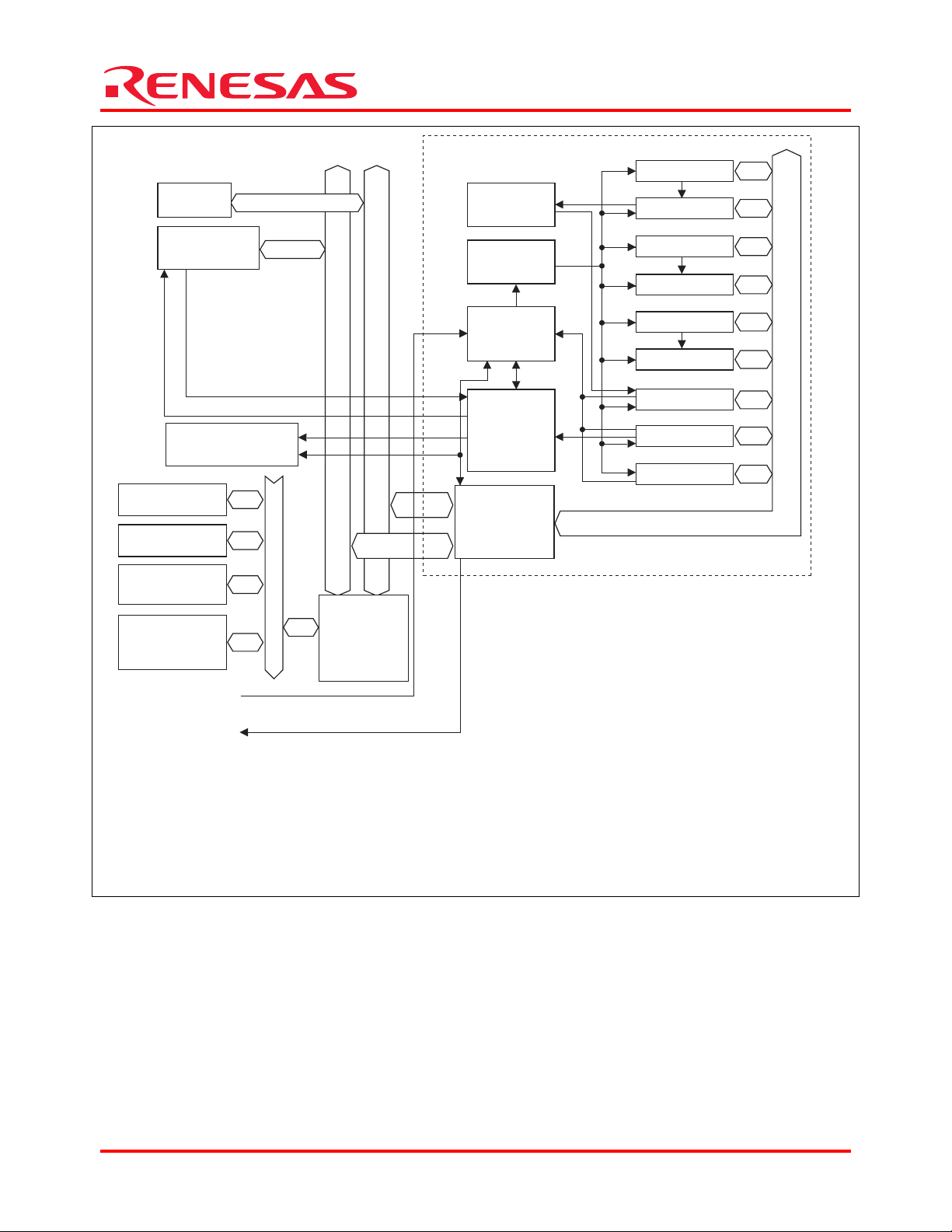
An overview of the DMAC is given in table 1. Also, a block diagram of the DMAC is shown in figure 1.
Table 1 Overview of DMAC
Item Description
Number of channels
Address space 4 Gbytes
Length of transfer data Byte, word (2 bytes), longword (4 bytes), and 16 bytes (longword × 4)
Maximum transfer
count
Address mode Single address mode and dual address mode
Transfer request Auto request, external request, and on-chip peripheral module request
Bus mode Cycle-stealing mode and burst mode
Priority level Channel priority fixed mode and round-robin mode
Interrupt request
External request
detection
Transfer request
acknowledge
signal/transfer end
signal
Note: For details on the DMAC, refer to the section on the direct memory access controller in the
SH7263/SH7203 Group Hardware Manual.
8 (CH0 to CH7)
Only 4 (CH0 to CH3) can receive external requests.
16,777,216 (24 bits) transfers
• SH7203/SH7263
(SCIF: 8 sources, I
sources, USB: 2 sources, FLCTL: 2 sources, RCAN-TL1: 2 sources, SSI: 4
sources, SSU: 4 sources)
• SH7263
(SRC: 2 sources, ROM-DEC: 1 sou rce, SDHI: 2 sources)
An interrupt request to the CPU is made when half or all of a transfer process is
completed.
DREQ input low/high level detection, rising/falling edge detection
Active levels for DACK and TEND can be set independently
2
C3: 8 sources, ADC: 1 source, MTU2: 5 sources, CMT: 2
REJ06B0734-0100/Rev.1.00 April 2008 Page 3 of 17
Page 4
On-chip
memory
On-chip
peripheral
module
SH7263/SH7203 Group
Data Transfer to On-chip Peripheral Modules with DMAC
DMAC module
RDMATCR_n
Iteration
control
Register
control
DMATCR_n
RSAR_n
SAR_n
DMA transfer acknowledge signal
Interrupt controller
External ROM
External RAM
External device
(memory mapped)
External device
(with acknowledge)
DREQ0 to DREQ3
DACK0 to DACK3,
TEND0, TEND1
DMA transfer
request signal
Internal bus
Peripheral bus
Bus state
controller
HEIn
DEIn
Start-up
control
Request
priority
control
Bus
interface
RDAR_n
DAR_n
CHCR_n
DMAOR
DMARS0 to DMARS3
[Legend]
RDMATCR: DMA reload transfer count register CHCR: DMA channel control register
DMATCR: DMA transfer count register DMAOR: DMA operation register
RSAR: DMA reload source address register DMARS0 to DMARS3: DMA extension resource selectors 0 to 3
SAR: DMA source address register HEIn: DMA transfer half-end interrupt request to the CPU
RDAR: DMA reload destination address register DEIn: DMA transfer end interrupt request to the CPU
DAR: DMA destination address register n: 0, 1, 2, 3, 4, 5, 6, 7
Figure 1 Block Diagram of DMAC
REJ06B0734-0100/Rev.1.00 April 2008 Page 4 of 17
Page 5
SH7263/SH7203 Group
Data Transfer to On-chip Peripheral Modules with DMAC
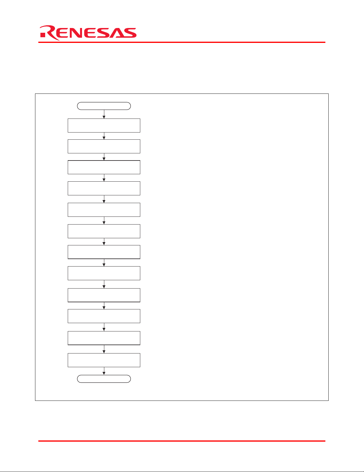
2.2 Procedure for Setting Used Modules
This section describes the procedure for making initial settings when the DMAC is to be used to transfer data from
memory to on-chip peripheral modules. On-chip peripheral module requests are used for transfer requests. A flowchart
of DMAC initialization is shown in figure 2. For details on registers, refer to the SH7263/SH7203 Group Hardware
Manual.
• Enabling clock supply to the DMAC (STBCR2)
[1]
START
Set standby control register 2
(STBCR2)
Set DMA channel control register
(CHCRn)
Set DMA source address control
register (SARn)
Set DMA reload source
address register (RSARn)
Set DMA destination address
register (DARn)
Set DMA reload destination
address register (RDARn)
Set DMA transfer count register
(DMATCRn)
Set DMA reload transfer
count register (RDMATCRn)
Set DMA channel control register
(CHCRn)
Set DMA extension resource selector
registers (DMARS0 to DMARS3)
Set DMA operation register
(DMAORn)
Set DMA channel control register
(CHCRn)
END
[1]
[2]
[3]
[4]
[5]
[6]
[7]
[8]
[9]
[10]
[11]
[12]
Clear the MSTP8 (module stop 8) bit to 0
[Function] Clock supply to the DMAC
• Disabling DMA transfer (CHCRn)
[2]
Clear the DE (DMA enable) bit to 0
[Function] Disable DMA transfer
• Setting DMA transfer source address (SARn)
[3]
[Function] Specify DMA transfer source address
• Setting DMA transfer source reload address (RSARn)
[4]
[Function] Specify DMA transfer source address to be reloaded
• Setting DMA transfer destination address (DARn)
[5]
[Function] Specify DMA transfer destination address
• Setting DMA transfer destination reload address (RDARn)
[6]
[Function] Specify DMA transfer destination address to be reloaded
• Setting the DMA transfer count (DMATCRn)
[7]
[Function] Set the DMA transfer count
• Setting the DMA transfer reload count (RDMATCRn)
[8]
[Function] Set the DMA transfer count to be reloaded
• Setting the DMA transfer mode (CHCRn)
[9]
Set the TC (transfer count mode) bit
[Function] "0": Transfer data once for each transfer request
(When the SCIF or IIC3 is selected as the transfer
"1": Transfer data for the count specified in DMATCRn for
Set the RLDSAR (SAR reload function enable/disable) bit
[Function] Enables/disables reload function to SAR and DMATCR
Set the RLDDAR (DAR reload function enable/disable) bit
[Function] Enables/disables reload function to DAR and DMATCR
Set the DM (destination address mode) bits
[Function] Select whether the DMA transfer destination address is
Fix/increment/decrement the DMA transfer destination address
Set the SM (source address mode) bits
[Function] Select whether the DMA transfer source address is
Fix/increment/decrement the DMA transfer source address
Set the RS (resource select) bits to B'1000.
[Function] Select DMA extension resource selector (DMA transfer
Set the TB (transfer bus mode) bit
[Function] Select a DMA transfer bus mode.
Cycle-stealing mode/burst mode
Note: When TC is set to 0, select cycle-stealing mode
Set the TS (transfer size) bits
[Function] Specify the DMA transfer size
Set the IE (interrupt enable) bit
[Function] Enable/disable interrupt requests
• Specifying settings for DMA transfer requests from on-chip peripheral
[10]
modules (DMARS0 to DMARS3)
[Function] Select the DMA transfer request source
SCIF, IIC3, A/D converter, MTU2, or CMT
• Setting the DMA operation register (DMAOR)
[11]
Read from the AE (address error flag) bit and then clear it to 0
[Function] Clear the address error flag
Read from the NMIF (NMI flag) bit and then clear it to 0
[Function] Clear the NMI flag
Set the DME (DMA master enable) bit to 1
[Function] Enable DMA transfer on all the channels
• Enablling DMA transfer (CHCRn)
[12]
Set the DE (DMA enable) bit to 1
[Function] Start DMA transfer
request source)
each transfer requests
incremented or decremented
incremented or decremented
request source)
Figure 2 Flowchart of Initializing DMAC
REJ06B0734-0100/Rev.1.00 April 2008 Page 5 of 17
Page 6
SH7263/SH7203 Group
Data Transfer to On-chip Peripheral Modules with DMAC
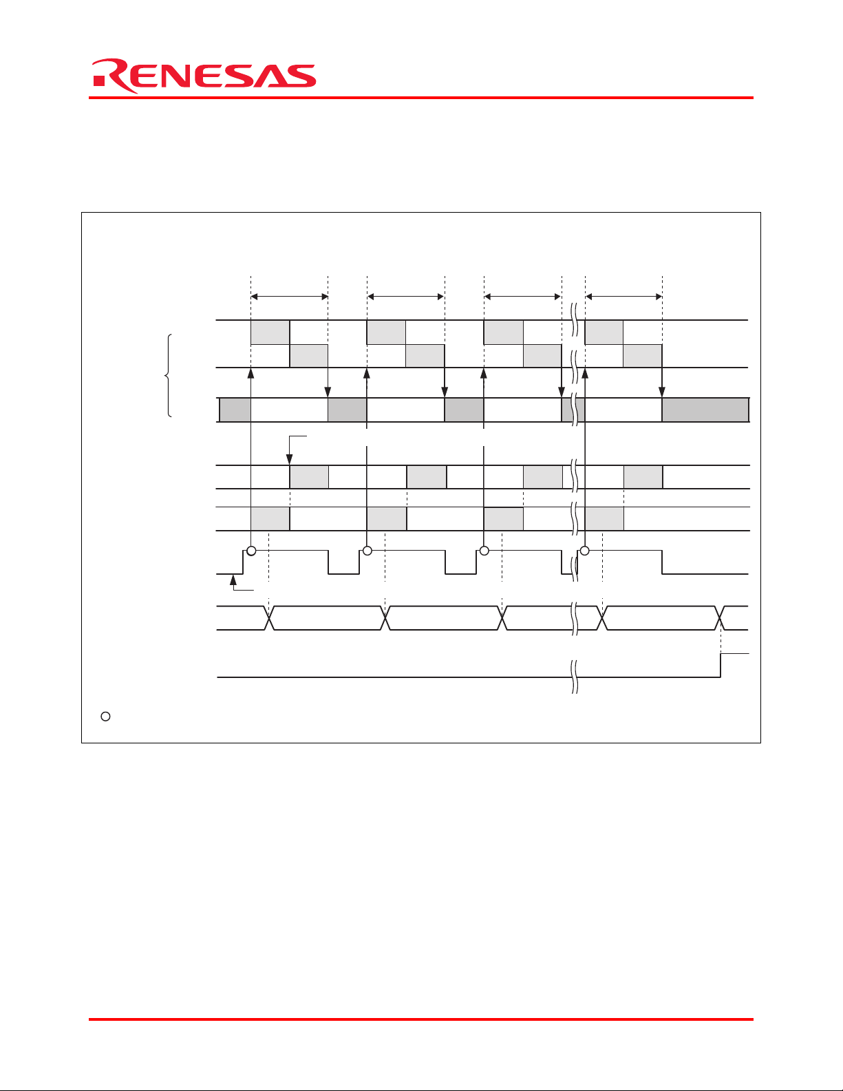
2.3 Operation of Sample Program
In this sample program, SCIF transmit FIFO data empty transfer requests are made to activate DMAC channel 1, and to
transfer data from external memory to the transmit FIFO data register (SCFTDR) on SCIF channel 0. The data written
to SCFTDR on SCIF channel 0 are transmitted in UART mode. An operation timing of the sample program is shown in
figure 3.
DMA transfer using SCIF transmit FIFO data empty transfer requests
(Timing of requesting data transfer from external memory to the SCIF transmit FIFO data register: a
transfer request is made when the number of data in transmit FIFO becomes 0)
DMAC1
Bus
mastership
CPU
Internal bus
External bus
DMA transfer request
(When the DMA master
enable bit is 1)
DMA transfer count
register (DMATCR)
Transfer end flag (TE)
One data
transfer
Read Read Read Read
Write Write Write Write
Write to SCIF transmit FIFO data register (SCFTDR)
Write Write Write Write
Read Read Read Read
SCIF transmit FIFO data empty transfer request (on-chip peripheral request)
H'28H'29
One data
transfer
Internal signal Internal signal Internal signal
One data
transfer
One data
transfer
H'27 H'00
[Legend]
: DMA request acknowledge
Figure 3 Operation Timing of Sample Application
REJ06B0734-0100/Rev.1.00 April 2008 Page 6 of 17
Page 7

SH7263/SH7203 Group
Data Transfer to On-chip Peripheral Modules with DMAC
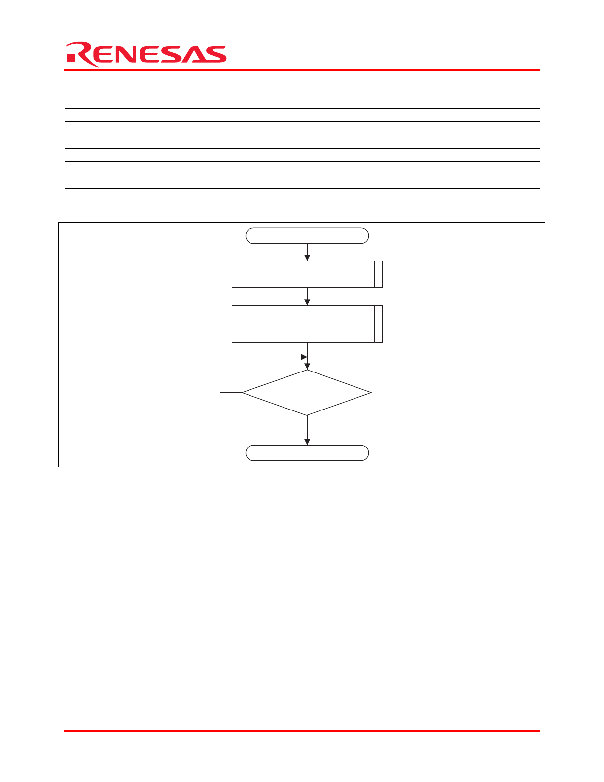
2.4 Processing Procedure of Sample Program
In this sample program, character string data stored in external memory are transferred by DMA to the transmit FIFO
data register (SCFTDR) on SCIF channel 0, and then are transmitted in UART mode.
The register settings for the sample program are listed in table 2. The macro definitions used in this sample program are
also listed in table 3. A flowchart of the sample program is illustrated in figure 4.
Table 2 Register Settings for Sample Program
Register Name Address Setting Value Description
Standby control
register 2 (STBCR2)
DMA channel control
register 1 (CHCR1)
DMA source address
register_1 (SAR1)
DMA destination
address register_1
(DAR1)
DMA transfer count
register_1 (DMATCR1)
DMA operation register
(DMAOR)
DMA extension
resource selector
(DMARS0)
H'FFFE 0018 H'00 MSTP8 = "0": DMAC operates
H'FFFE 101C
H'FFFE 1010
H'FFFE 1014 H'FFFE 800C
H'FFFE 1018
H'FFFE 1200 H'0001
H'FFFE 1300 H'0081 MID = "B'100000"
H'0000 0000 DE = "0": Di sa b l es D M A t r an s f e r
H'0000 1800
H'0000 1801 DE = "1": En a bl e s D M A t r an s f e r
Address where
character string
data are stored
Number of
character string
data
TC = "0 ": Transfers data once for each
DMA transfer request
RLDSAE = "0":
Disables SAR reload function
RLDDAR = "0":
Disables DAR reload function
DM = "B' 0 0" : Fixes destination address
SM = "B'01": Increments source address
RS = "B'1000": Extension resource selector
TB = "0": Cycle-stealing mode
TS = "B'00": Byte transfer
IE = "0": Disables interrupt request
Start address of transfer source:
Start address of character string stored in
external memory
Start address of transfer destination:
Address of the SCIF transmit FIFO data
register_1 (SCFTDR_1)
Transfer count: the number of character
string data
DME = "1": Enables DMA transfer on all the
channels
RID = "B'01"
Set to SCIF_0 transmit FIFO data empty
transfer request
REJ06B0734-0100/Rev.1.00 April 2008 Page 7 of 17
Page 8
SH7263/SH7203 Group
Data Transfer to On-chip Peripheral Modules with DMAC
Table 3 Macro Definitions Used in Sample Program
Macro Definition Setting Value Description
DMA_SIZE_BYTE H'0000 Byte transfer
DMA_SIZE_WORD H'0001 Word transfer
DMA_SIZE_LONG H'0002 Longword transfer
DMA_SIZE_LONGx4 H'0003 16-byte transfer
DMA_INT_DISABLE H'0000 DMA transfer end interrupt disabled
DMA_INT_ENABLE H'0010 DMA transfer end interrupt enabled
START
Initialize DMAC/enable transfer
transmission and transmission
No
io_init_dma1()
Initialize SCIF/enable
interrupts
io_init_scif()
DMA transfer
completed?
Yes
END
Figure 4 Flowchart of Sample Program
REJ06B0734-0100/Rev.1.00 April 2008 Page 8 of 17
Page 9

SH7263/SH7203 Group
Data Transfer to On-chip Peripheral Modules with DMAC
3. Sample Program
1. Sample Program Listing "main.c" (1)
1 /*""FILE COMMENT""**************************************************************
2 *
3 * System Name : SH7203 Sample Program
4 * File Name : main.c
5 * Contents : Data transfer to on-chip peripheral modules with DMAC
6 * Version : 1.00.00
7 * Model : M3A-HS30
8 * CPU : SH7203
9 * Compiler : SHC9.1.1.0
10 * note : Sample program for transferring data from the SCIF by DMAC1
11 *
12 * <CAUTION>
13 * This sample program is for reference
14 * and its operation is not guaranteed.
15 * Customers should use this sample program for technical reference
16 * in software development.
17 *
18 * The information described here may contain technical inaccuracies or
19 * typographical errors. Renesas Technology Corporation and Renesas Solutions
20 * assume no responsibility for any damage, liability, or other loss rising
21 * from these inaccuracies or errors.
22 *
23 * Copyright(C) 2007 Renesas Technology Corp. All Rights Reserved
24 * AND Renesas Solutions Corp. All Rights Reserved
25 *
26 * history : 2007.12.27 ver.1.00.00
27 *""FILE COMMENT END""*********************************************************/
28 #include <string.h>
29 #include "iodefine.h" /* iodefine.h is automatically created by HEW */
30
31 /* ==== Macro declaration ==== */
32 /* ====
33 #define DMA_SIZE_BYTE 0x0000u
34 #define DMA_SIZE_WORD 0x0001u
35 #define DMA_SIZE_LONG 0x0002u
36 #define DMA_SIZE_LONGx4 0x0003u
37 #define DMA_INT_DISABLE 0x0000u
38 #define DMA_INT_ENABLE 0x0010u
39 #define DMA_INT (DMA_INT_ENABLE >> 4u)
40
41 /* ==== Prototype declaration ==== */
42 void main(void);
43 void io_init_dma1(void *src, void *dst, size_t size, unsigned int mode);
44 void io_dma1_stop(void);
45 void io_init_scif0(int);
46
47 /* ==== Type declaration ==== */
48 /* SCIF baud rate setting */
49 typedef struct {
50 unsigned char scbrr;
51 unsigned short scsmr;
52 } SH7203_BAUD_SET;
53
DMAC Settings ==== */
REJ06B0734-0100/Rev.1.00 April 2008 Page 9 of 17
Page 10

SH7263/SH7203 Group
Data Transfer to On-chip Peripheral Modules with DMAC
2. Sample Program Listing "main.c" (2)
54 /* ---- Values for baud rate specification ---- */
55 enum{
56 CBR_1200,
57 CBR_2400,
58 CBR_4800,
59 CBR_9600,
60 CBR_19200,
61 CBR_31250,
62 CBR_38400,
63 CBR_57600,
64 CBR_115200
65 };
66
67 /* ==== Table of register setting values ==== */
68 static SH7203_BAUD_SET scif_baud[] = {
69 {214, 1}, /* 1200bps (-0.07%) */
70 {106, 1}, /* 2400bps ( 0.39%) */
71 {214, 0}, /* 4800bps (-0.07%) */
72 {106, 0}, /* 9600bps ( 0.39%) */
73 { 53, 0}, /* 19200bps (-0.54%) */
74 { 32, 0}, /* 31250bps ( 0.00%) */
75 { 26, 0}, /* 38400bps (-0.54%) */
76 { 17, 0}, /* 57600bps (-0.54%) */
77 { 8, 0} /*115200bps (-0.54%) */
78 };
79 /* Character string to be transmitted */
80 const signed char data[] = "SCIF request DMAC Sample Software SH7203.¥r¥n";
81
82 /*""FUNC COMMENT""*******************************************************
83 * Outline : Sample Program Main (UART transmission with use of DMAC)
84 *----------------------------------------------------------------------85 * Include : #include <string.h>
86 *----------------------------------------------------------------------87 * Declaration : void main(void);
88 *----------------------------------------------------------------------89 * Function : The character string data stored in external memory is DMA transferred
90 * : to the SCIF transmit FIFO data register. The DMAC is activated
91 * : by an SCIF transmit interrupt request.
92 *----------------------------------------------------------------------93 * Argument : void
94 *----------------------------------------------------------------------95 * Return Value : void
96 *----------------------------------------------------------------------97 * Notice :
98 *""FUNC COMMENT END""***************************************************/
99 void main(void)
100 {
101 /* ==== Enabling DMAC initialization/transfer ==== */
102 io_init_dma1(data, (void *)&SCIF0.SCFTDR.BYTE ,sizeof(data),
103 DMA_SIZE_BYTE | DMA_INT_DISABLE);
104 /* On-chip peripheral module request (SCIF transmit interrupt request) */
105 /* Data transfer from external memory to SCIF transmit */
106 /* Data transfer to data registers */
REJ06B0734-0100/Rev.1.00 April 2008 Page 10 of 17
Page 11

SH7263/SH7203 Group
Data Transfer to On-chip Peripheral Modules with DMAC
3. Sample Program Listing "main.c" (3)
107 /* ==== Enabling SCIF0 initialization/transfer ==== */
108 io_init_scif0(CBR_115200);
109 /* Communication mode :UART mode */
110 /* Bit rate :115.2Kbps */
111 /* TXI interrupt is generated when data in transmit FIFO is one byte */
112 /* ==== Disabling DMA transfer ==== */
113 io_dma1_stop();
114 while(1){
115 /* Program end */
116 }
117 }
118 /*""FUNC COMMENT""*******************************************************
119 * Outline : Initialization for DATA transfer between memory areas with DMAC
120 *----------------------------------------------------------------------121 * Include : #include "iodefine.h"
122 *----------------------------------------------------------------------123 * Declaration : io_init_dma1(void *src, void *dst, size_t size, int mode);
124 *----------------------------------------------------------------------125 * Function :
126 * :
127 * :
128 * :
129 *----------------------------------------------------------------------130 * Argument : void *src :
131 * : void *dst :
132 * : size_t size : Transfer size (byte)
133 * :
134 * : DMA_SIZE_BYTE (0x0000)
135 * : DMA_SIZE_WORD (0x0001)
136 * : DMA_SIZE_LONG (0x0002)
137 * : DMA_SIZE_LONGx4(0x0003) 16-byte transfer
138 * : DMA_INT_DISABLE(0x0000)
139 * : DMA_INT_ENABLE (0x0010) DMA transfer end interrupt disabled
140 *----------------------------------------------------------------------141 * Return Value : void
142 *----------------------------------------------------------------------143 * Notice :
144 * : address is inconsistent.
145 * : When interrupts are used, interrupt routines must be registered.
146 *""FUNC COMMENT END""***************************************************/
147 void io_init_dma1(void *src, void *dst, size_t size, unsigned int mode)
148 {
149 unsigned int ts;
150 unsigned long ie;
151
152 ts = mode & 0x3u;
153 ie = (mode & 0x00f0u ) >> 4u;
154
155 /* ====Setting standby control register 2(STBCR2) ==== */
156 CPG.STBCR2.BIT.MSTP8 = 0x0; /* Cancel DMAC module top mode */
157
158 /* ---- Setting DMA channel control register ---- */
159 DMAC.CHCR1.BIT.DE = 0ul; /* Disable DMA transfer */
160
The DMAC transfers the amount of data specified by “size”.
from the source address “src” to the destination address “dst.”
Transfer is performed using requests from the SCIF1.
“mode” is specified for transfer size and interrupt used/not used.
Source address
Destination address
unsigned int mode: Transfer mode, specifies the following with logical OR.
Byte transfer
Word transfer
Longword transfer
DMA transfer end interrupt disabled
Operation is not guaranteed when the alignment of the source/destination.
REJ06B0734-0100/Rev.1.00 April 2008 Page 11 of 17
Page 12

SH7263/SH7203 Group
Data Transfer to On-chip Peripheral Modules with DMAC
4. Sample Program Listing "main.c" (4)
161 /* ----Setting DMA source address register---- */
162 DMAC.SAR1.LONG = (unsigned long)src;
163
164 /* ----Setting DMA reload source address register---- */
165 DMAC.RSAR1.LONG = (unsigned long)src;
166
167 /* ----Setting DMA destination address register---- */
168 DMAC.DAR1.LONG = (unsigned long)dst;
169
170 /* ----Setting DMA reload destination address register---- */
171 DMAC.RDAR1.LONG = (unsigned long)dst;
172
173 /* ----Setting DMA transfer count register---- */
174 /* ----Setting DMA reload transfer count register---- */
175
176 switch(ts){
177 case DMA_SIZE_BYTE:
178 DMAC.DMATCR0.LONG = size; /*
179 DMAC.RDMATCR0.LONG = size;
180 break;
181 case DMA_SIZE_WORD:
182 DMAC.DMATCR0.LONG = size >> 1u; /*
183 DMAC.RDMATCR0.LONG = size >> 1u;
184 break;
185 case DMA_SIZE_LONG:
186 DMAC.DMATCR0.LONG = size >> 2u; /*
187 DMAC.RDMATCR0.LONG = size >> 2u;
188 break;
189 case DMA_SIZE_LONGx4:
190 DMAC.DMATCR0.LONG = size >> 4u; /*
191 DMAC.RDMATCR0.LONG = size >> 4u;
192 break;
193 default:
194 break;
195 }
196
197 /* ----Setting DMA channel control register---- */
198 DMAC.CHCR1.LONG = 0x00001800ul | (ts << 3u) | (ie << 2u) ;
199 /*
200 bit31 : TC DMATCR transfer0--------- Transfer once
201 bit30 : reserve 0
202 bit29 : RLDSAR OFF : 0------------- Disable SAR reload function
203 bit28 : RLDDAR OFF : 0------------- Disable DAR reload function
204 bit27-24 : reserve 0
205 bit23 : DO over run0 : 0---------- Unused
206 bit22 : TL TEND low active : 0---- Unused
207 bit21 : reserve 0
208 bit20 : TEMASK : TE set mask : 0-- Disable DMA transfer when TE bit is set
209 bit19 : HE :0--------------------- Unused
210 bit18 : HIE :0-------------------- Unused
211 bit17 : AM :0--------------------- Unused
212 bit16 : AL :0--------------------- Unused
213 bit15-14 : DM1:0 DM0:0--------------- Fix destination address
214 bit13-12 : SM1:0 SM0:1--------------- Increment source address
215 bit11-8 : RS : auto request : B'1000- DMA extension resource selector
216 bit7 : DL : DREQ level : 0 ------- Unused
Specify transfer count (1/1) */
Specify transfer count (1/2) */
Specify transfer count (1/4) */
Specify transfer count (1/16) */
REJ06B0734-0100/Rev.1.00 April 2008 Page 12 of 17
Page 13

SH7263/SH7203 Group
Data Transfer to On-chip Peripheral Modules with DMAC
5. Sample Program Listing "main.c" (5)
217 bit6 : DS : DREQ select :0 Low level Unused
218 bit5 : TB : cycle :0--------------- Cycle-stealing mode
219 bit4-3 : TS : transfer size:B'00--- Byte transfer
220 bit2 : IE : interrupt enable:0--- Disable interrupt
221 bit1 : TE : transfer end----------
222 bit0 : DE : DMA enable bit:0----- DMA
223 */
224
225 /* ----Setting DMA extension resource selector 0---- */
226 DMAC.DMARS0.BIT.CH1MID = 0x20; /* MID = SCIF0 */
227 DMAC.DMARS0.BIT.CH1RID = 0x01; /* RID = Transmission */
228
229 /* ----Setting DMA operation register---- */
230 DMAC.DMAOR.WORD &= 0xfff9u; /* Clear AE,NMI bits */
231
232 if(DMAC.DMAOR.BIT.DME == 0ul){ /* Enable DMA transfer on all channels */
233 DMAC.DMAOR.BIT.DME = 1ul;
234 }
235
236 /* ----DMA transfer execution---- */
237 DMAC.CHCR1.BIT.DE = 1ul; /* Enable DMA transfer */
238 }
239 /*""FUNC COMMENT""*******************************************************
240 * Outline : DMAC stop
241 *----------------------------------------------------------------------242 * Include : #include "iodefine.h"
243 *----------------------------------------------------------------------244 * Declaration : void io_dma1_stop(void);
245 *----------------------------------------------------------------------246 * Function : Detects the end of DMA transfer and disables DMA transfer
247 *----------------------------------------------------------------------248 * Argument : void
249 *----------------------------------------------------------------------250 * Return Value: void
251 *----------------------------------------------------------------------252 * Notice :
253 *""FUNC COMMENT END""***************************************************/
254 void io_dma1_stop(void)
255 {
256 /* Detecting end of transfer */
257 while(DMAC.CHCR1.BIT.TE == 0ul){
258 /* Wait until the TE bit is set*/
259 }
260
261 /* ----Stopping DMA transfer---- */
262 DMAC.CHCR1.BIT.DE = 0ul; /* Disable DMA1 transfer */
263 }
264
265 /*""FUNC COMMENT""*******************************************************
266 * Outline : Initial setting of SCIF0 as an asynchronous (UART) transmit module
267 *----------------------------------------------------------------------268 * Include : #include "iodefine.h"
269 *----------------------------------------------------------------------270 * Declaration : void io_init_scif0(int bps);
271 *-----------------------------------------------------------------------
REJ06B0734-0100/Rev.1.00 April 2008 Page 13 of 17
Page 14

SH7263/SH7203 Group
Data Transfer to On-chip Peripheral Modules with DMAC
6. Sample Program Listing "main.c" (7)
272 * Function : Initializes SCIF0
273 * : Asynchronous (UART)/ 8 bits/ No parity/ 1 stop bit/ RTS/CTS disabled
274 * : Baud rate is specified by argument bps
275 * :
276 *----------------------------------------------------------------------277 * Argument : int bps : Value for baud rate specification
278 *----------------------------------------------------------------------279 * Return Value: void
280 *----------------------------------------------------------------------281 * Notice : The baud rate setting values given in this program are those when
282 * : the peripheral module clock (Pf) frequency is 33 MHz. If a different
283 * : clock is used, the baud rate setting values must be changed.
284 *""FUNC COMMENT END""***************************************************/
285 void io_init_scif0(int bps)
286 {
287 /* ====Power-down mode cancellation==== */
288 /* ----Setting standby control register 4 (STBCR4)---- */
289 CPG.STBCR4.BIT.MSTP47 = 0; /* Start clock supply to SCIF0 */
290
291 /* ====SCIF0 initialization==== */
292 /* ----Setting serial control register (SCSCRi)---- */
293 SCIF0.SCSCR.WORD = 0x0000; /* Stop transmission/reception by SCIF0 */
294
295 /* ----Setting FIFO control register (SCFCRi)---- */
296 SCIF0.SCFCR.BIT.TFRST = 1; /* Reset transmit FIFO */
297
298 /* ----Setting serial control register (SCSCRi)---- */
299 SCIF0.SCSCR.BIT.CKE = 0x0; /* B'00: Internal clock */
300
301 /* ----Setting serial mode register (SCSMRi)---- */
302 SCIF0.SCSMR.WORD = scif_baud[bps].scsmr;
303 /* Communication mode 0: Asynchronous mode */
304 /* Character length 0: 8-bit data */
305 /* Parity enable 0: Disable addition and check */
306 /* Parity mode 0: Even parity */
307 /* Stop bit length 0: 1 stop bit */
308 /* Clock select : Table value */
309
310 /* ----Setting bit rate register (SCBRRi)---- */
311 SCIF0.SCBRR.BYTE = scif_baud[bps].scbrr;
312
313 /* ----Setting FIFO control register (SCFCRi)---- */
314 SCIF0.SCFCR.WORD = 0x0030; /* Transmit FIFO data count trigger
315 : Number of data bytes = 0 */
316 /* Modem control enable : Disabled */
317 /* Transmit FIFO data register reset : Disabled */
318 /* Loopback test : Disabled */
319
319 /* ====Setting pin function controller (PFC)==== */
320 PORT.PECRL1.BIT.PE1MD = 0x3; /* Switch to TxD0 pin */
321
322 /* ----Setting serial control register (SCSCRi) ---- */
323 SCIF0.SCSCR.BIT.TIE = 1; /* Enable SCIF0 transmit interrupt */
324 SCIF0.SCSCR.BIT.TE = 1; /* Enable SCIF0 transmission */
325
326 }
327 /* End of File */
REJ06B0734-0100/Rev.1.00 April 2008 Page 14 of 17
Page 15

SH7263/SH7203 Group
Data Transfer to On-chip Peripheral Modules with DMAC
4. Documents for Reference
• Software Manual
SH-2A, SH2A-FPU Software Manual
The most up-to-date version of this document is available on the Renesas Technology Website.
• Hardware Manual
SH7203 Group Hardware Manual
SH7263 Group Hardware Manual
The most up-to-date version of this document is available on the Renesas Technology Website.
REJ06B0734-0100/Rev.1.00 April 2008 Page 15 of 17
Page 16

Website and Support
Renesas Technology Website
http://www.renesas.com/
Inquiries
http://www.renesas.com/inquiry
csc@renesas.com
Revision Record
SH7263/SH7203 Group
Data Transfer to On-chip Peripheral Modules with DMAC
Rev.
1.00 Apr.17.08 — First edition issued
All trademarks and registered trademarks are the property of their respective owners.
Date
Description
Page Summary
REJ06B0734-0100/Rev.1.00 April 2008 Page 16 of 17
Page 17

SH7263/SH7203 Group
Data Transfer to On-chip Peripheral Modules with DMAC
Notes regarding these materials
1. This document is provided for reference purposes only so that Renesas customers may select the appropriate
Renesas products for their use. Renesas neither makes warranties or representations with respect to the
accuracy or completeness of the information contained in this document nor grants any license to any intellectual
property rights or any other rights of Renesas or any third party with respect to the information in this document.
2. Renesas shall have no liability for damages or infringement of any intellectual property or other rights arising out
of the use of any information in this document, including, but not limited to, product data, diagrams, charts,
programs, algorithms, and application circuit examples.
3. You should not use the products or the technology described in this document for the purpose of military
applications such as the development of weapons of mass destruction or for the purpose of any other military
use. When exporting the products or technology described herein, you should follow the applicable export
control laws and regulations, and procedures required by such laws and regulations.
4. All information included in this document such as product data, diagrams, charts, programs, algorithms, and
application circuit examples, is current as of the date this document is issued. Such information, however, is
subject to change without any prior notice. Before purchasing or using any Renesas products listed in this
document, please confirm the latest product information with a Renesas sales office. Also, please pay regular
and careful attention to additional and different information to be disclosed by Renesas such as that disclosed
through our website. (http://www.renesas.com)
5. Renesas has used reasonable care in compiling the information included in this document, but Renesas
assumes no liability whatsoever for any damages incurred as a result of errors or omissions in the information
included in this document.
6. When using or otherwise relying on the information in this document, you should evaluate the information in light
of the total system before deciding about the applicability of such information to the intended application.
Renesas makes no representations, warranties or guaranties regarding the suitability of its products for any
particular application and specifically disclaims any liability arising out of the application and use of the
information in this document or Renesas products.
7. With the exception of products specified by Renesas as suitable for automobile applications, Renesas products
are not designed, manufactured or tested for applications or otherwise in systems the failure or malfunction of
which may cause a direct threat to human life or create a risk of human injury or which require especially high
quality and reliability such as safety systems, or equipment or systems for transportation and traffic, healthcare,
combustion control, aerospace and aeronautics, nuclear power, or undersea communication transmission. If you
are considering the use of our products for such purposes, please contact a Renesas sales office beforehand.
Renesas shall have no liability for damages arising out of the uses set forth above.
8. Notwithstanding the preceding paragraph, you should not use Renesas products for the purposes listed below:
(1) artificial life support devices or systems
(2) surgical implantations
(3) healthcare intervention (e.g., excision, administration of medication, etc.)
(4) any other purposes that pose a direct threat to human life
Renesas shall have no liability for damages arising out of the uses set forth in the above and purchasers who
elect to use Renesas products in any of the foregoing applications shall indemnify and hold harmless Renesas
Technology Corp., its affiliated companies and their officers, directors, and employees against any and all
damages arising out of such applications.
9. You should use the products described herein within the range specified by Renesas, especially with respect to
the maximum rating, operating supply voltage range, movement power voltage range, heat radiation
characteristics, installation and other product characteristics. Renesas shall have no liability for malfunctions or
damages arising out of the use of Renesas products beyond such specified ranges.
10. Although Renesas endeavors to improve the quality and reliability of its products, IC products have specific
characteristics such as the occurrence of failure at a certain rate and malfunctions under certain use conditions.
Please be sure to implement safety measures to guard against the possibility of physical injury, and injury or
damage caused by fire in the event of the failure of a Renesas product, such as safety design for hardware and
software including but not limited to redundancy, fire control and malfunction prevention, appropriate treatment
for aging degradation or any other applicable measures. Among others, since the evaluation of microcomputer
software alone is very difficult, please evaluate the safety of the final products or system manufactured by you.
11. In case Renesas products listed in this document are detached from the products to which the Renesas products
are attached or affixed, the risk of accident such as swallowing by infants and small children is very high. You
should implement safety measures so that Renesas products may not be easily detached from your products.
Renesas shall have no liability for damages arising out of such detachment.
12. This document may not be reproduced or duplicated, in any form, in whole or in part, without prior written
approval from Renesas.
13. Please contact a Renesas sales office if you have any questions regarding the information contained in this
document, Renesas semiconductor products, or if you have any other inquiries.
2008. Renesas Technology Corp., all rights reserved.
REJ06B0734-0100/Rev.1.00 April 2008 Page 17 of 17
 Loading...