

Page 1

Renesas 32-Bit Single-Chip RISC Microprocessor
SuperH RISC engine Family/SH7040 Series
(CPU Core SH-2)
Rev.6.00
2003.5.26
SH7040, SH7041, SH7042,
SH7043, SH7044, SH7055
Group
Hardware Manual
32
查询SH7040A供应商
Page 2

Page 3

Renesas 32-Bit Single-Chip RISC
Microprocessor
SuperH RISC engine Family/
SH7040 Series (CPU Core SH-2)
SH7040, SH7041, SH7042,
SH7043, SH7044, SH7055
Group
Hardware Manual
REJ09B0044-0600O
Page 4

Cautions
Keep safety first in your circuit designs!
1 . Renesas Technology Corporation puts the maximum effort into making semiconductor products better and more reliable, but
there is always the possibility that trouble may occur with them. Trouble with semiconductors may lead to personal injury, fire or
property damage.
Remember to give due consideration to safety when making your circuit designs, with appropriate measures such as (i) placement
of substitutive, auxiliary circuits, (ii) use of nonflammable material or (iii) prevention against any malfunction or mishap.
Notes regarding these materials
1 . These materials are intended as a reference to assist our customers in the selection of the Renesas Technology Corporation
product best suited to the customer's application; they do not convey any license under any intellectual property rights, or any
other rights, belonging to Renesas Technology Corporation or a third party.
2 . Renesas Technology Corporation assumes no responsibility for any damage, or infringement of any third-party's rights,
originating in the use of any product data, diagrams, charts, programs, algorithms, or circuit application examples contained in
these materials.
3 . All information contained in these materials, including product data, diagrams, charts, programs and algorithms represents
information on products at the time of publication of these materials, and are subject to change by Renesas Technology
Corporation without notice due to product improvements or other reasons. It is therefore recommended that customers contact
Renesas Technology Corporation or an authorized Renesas Technology Corporation product distributor for the latest product
information before purchasing a product listed herein.
The information described here may contain technical inaccuracies or typographical errors.
Renesas Technology Corporation assumes no responsibility for any damage, liability, or other loss rising from these inaccuracies
or errors.
Please also pay attention to information published by Renesas Technology Corporation by various means, including the
Renesas Technology Corporation Semiconductor home page (http://www.renesas.com).
4 . When using any or all of the information contained in these materials, including product data, diagrams, charts, programs, and
algorithms, please be sure to evaluate all information as a total system before making a final decision on the applicability of the
information and products. Renesas Technology Corporation assumes no responsibility for any damage, liability or other loss
resulting from the information contained herein.
5 . Renesas Technology Corporation semiconductors are not designed or manufactured for use in a device or system that is used
under circumstances in which human life is potentially at stake. Please contact Renesas Technology Corporation or an
authorized Renesas Technology Corporation product distributor when considering the use of a product contained herein for any
specific purposes, such as apparatus or systems for transportation, vehicular, medical, aerospace, nuclear, or undersea repeater
use.
6 . The prior written approval of Renesas Technology Corporation is necessary to reprint or reproduce in whole or in part these
materials.
7 . If these products or technologies are subject to the Japanese export control restrictions, they must be exported under a license
from the Japanese government and cannot be imported into a country other than the approved destination.
Any diversion or reexport contrary to the export control laws and regulations of Japan and/or the country of destination is
prohibited.
8 . Please contact Renesas Technology Corporation for further details on these materials or the products contained therein.
Page 5

Preface
The SH7040 Series (SH7040, SH7041, SH7042, SH7043, SH7044, SH7045) single-chip RISC
(Reduced Instruction Set Computer) microprocessors integrate a Renesas Technology-original
RISC CPU core with peripheral functions required for system configuration.
The CPU has a RISC-type instruction set. Most instructions can be executed in one clock cycle,
which greatly improves instruction execution speed. In addition, the 32-bit internal-bus
architecture enhances data processing power. With this CPU, it has become possible to assemble
low cost, high performance/high-functioning systems, even for applications that were previously
impossible with microprocessors, such as real-time control, which demands high speeds. In
particular, the SH7040 series has a 1-kbyte on-chip cache, which allows an improvement in CPU
performance during external memory access.
In addition, the SH7040 series includes on-chip peripheral functions necessary for system
configuration, such as large-capacity ROM and RAM, timers, a serial communication interface
(SCI), an A/D converter, an interrupt controller, and I/O ports. Memory or peripheral LSIs can be
connected efficiently with an external memory access support function. This greatly reduces
system cost.
There are versions of on-chip ROM: mask ROM, PROM, and flash memory. The flash memory
can be programmed with a programmer that supports SH7040 series programming, and can also
be programmed and erased by software.
This hardware manual describes the SH7040 series hardware. Refer to the programming manual
for a detailed description of the instruction set.
Related Manual
SH7040 series instructions
SH-1/SH-2/SH-DSP Programming Manual
Please consult your Renesas Technology sales representative for details for development
environment system.
Page 6

Page 7
List of Items Revised or Added for This Version
Section Page Description
1.1.1 SH7040 Series
Features
Notes on the
SH7040 Series
Specifications
7,
9
Type Abbreviation Package Frequency Voltage Type Name ROM
ZTAT SH7042 128 kB 16 bits ±15LSB
FLASH SH7044F 256 kB 16 bits ±4LSB
MASK SH7040A 64 kB 16 bits ±4LSB
ROM
less
Note: Package with Copper used as the lead material.
Mask
Version
SH7042A A mask
SH7043 128 kB 32 bits ±15LSB
SH7043A A mask 128 kB 32 bits ±4LSB
A mask
SH7045F A mask 256 kB 32 bits ±4LSB
A mask
SH7041A A mask 64 kB 32 bits ±4LSB
SH7042 128 kB 16 bits ±15LSB
SH7042A A mask 128 kB 16 bits ±4LSB
SH7043 128 kB 32 bits ±15LSB
SH7043A A mask 128 kB 32 bits ±4LSB
SH7044 A mask 256 kB 16 bits ±4LSB
SH7045 A mask 256 kB 32bits ±4LSB
A mask
SH7040A 16 bits ±4LSB
SH7041A A mask 32 bits ±4LSB
A/D
External
Bus Width
Accuracy
(5Vversion)
(High-Speed)
(Mid-Speed)
(High-Speed)
(Mid-Speed)
(Mid-Speed)
(Mid-Speed)
(Mid-Speed)
(Mid-Speed)
(High-Speed)
(Mid-Speed)
(High-Speed)
(Mid-Speed)
(Mid-Speed)
(Mid-Speed)
(Mid-Speed)
(Mid-Speed)
On-chip
ROM
128 kB 16 bits ±4LSB
Operating
Temp
QFP2020-112 –20°C to 75°C 28 MHz
–20°C to 75°C 28 MHz
QFP2020-112
TQFP1414-120
QFP2020-112Cu*
QFP2020-144 –20°C to 75°C 28 MHz
QFP2020-144
–20°C to 75°C 28 MHz
QFP2020-144Cu*
QFP2020-112 –20°C to 75°C 28 MHz 5 V HD64F7044F28 See “256 kB Flash
QFP2020-144 –20°C to 75°C 28 MHz 5 V HD64F7045F28 See “256 kB Flash
–20°C to 75°C 28 MHz
QFP2020-112
TQFP1414-120
QFP2020-112Cu*
QFP2020-144
–20°C to 75°C 28 MHz
QFP2020-144Cu*
QFP2020-112 –20°C to 75°C 28 MHz
QFP2020-112
–20°C to 75°C 28 MHz
TQFP1414-120
QFP2020-112Cu*
QFP2020-144 –20°C to 75°C 28 MHz
QFP2020-144
–20°C to 75°C 28 MHz
QFP2020-144Cu*
QFP2020-112 –20°C to 75°C 28 MHz 5 V HD6437044F28 See “256 kB Mask
QFP2020-144 –20°C to 75°C 28 MHz 5 V HD6437045F28 See “256 kB Mask
–20°C to 75°C 28 MHz
QFP2020-112
TQFP1414-120
QFP2020-112Cu*
QFP2020-144
–20°C to 75°C 28 MHz
QFP2020-144Cu*
16 MHz
16 MHz
16 MHz
28 MHz
16 MHz
16 MHz
16 MHz
28 MHz
16 MHz
16 MHz
16 MHz
28 MHz
16 MHz
16 MHz
28 MHz
16 MHz
16 MHz
16 MHz
16 MHz
28 MHz
16 MHz
16 MHz
16 MHz
28 MHz
16 MHz
16 MHz
16 MHz
28 MHz
16 MHz
16 MHz
28 MHz
16 MHz
5 V
3.3 V
5 V
3.3 V
3.3 V
5 V
3.3 V
5 V
3.3 V
5 V
3.3 V
5 V
3.3 V
5 V
3.3 V
3.3 V
5 V
3.3 V
5 V
3.3 V
5 V
3.3 V
5 V
3.3 V
5 V
3.3 V
3.3 V
5 V
3.3 V
5 V
3.3 V
5 V
3.3 V
5 V
3.3 V
5 V
3.3 V
3.3 V
5 V
3.3 V
5 V
3.3 V
5 V
3.3 V
HD6477042F28
HD6477042VF16
HD6477042AF28
HD6477042AVF16
HD6477042AVX16
HD6477042ACF28
HD6477042AVCF16
HD6477043F28
HD6477043VF16
HD6477043AF28
HD6477043AVF16
HD6477043ACF28
HD6477043AVCF16
HD6437040AF28
HD6437040AVF16
HD6437040AVX16
HD6437040ACF28
HD6437040AVCF16
HD6437041AF28
HD6437041AVF16
HD6437041ACF28
HD6437041AVCF16
HD6437042F28
HD6437042VF16
HD6437042AF28
HD6437042AVF16
HD6437042AVX16
HD6437042ACF28
HD6437042AVCF16
HD6437043F28
HD6437043VF16
HD6437043AF28
HD6437043AVF16
HD6437043ACF28
HD6437043AVCF16
HD6417040AF28
HD6417040AVF16
HD6417040AVX16
HD6417040ACF28
HD6417040AVCF16
HD6417041AF28
HD6417041AVF16
HD6417041ACF28
HD6417041AVCF16
Notes on the SH7040 Series Specifications
See “128 kB
PROM”
See “128 kB
PROM”
See “128 kB
PROM”
See “128 kB
PROM”
Memory”
Memory”
See “64 kB Mask
ROM”
See “64 kB Mask
ROM”
See “128 kB Mask
ROM”
See “128 kB Mask
ROM”
See “128 kB Mask
ROM”
See “128 kB Mask
ROM”
ROM”
ROM”
Electrical
Characteristics
See “Electrical
Characteristics”
See “Electrical
Characteristics”
See “Electrical
Characteristics”
See “Electrical
Characteristics”
See “Electrical
Characteristics”
See “Electrical
Characteristics”
See “Electrical
Characteristics”
See “Electrical
Characteristics”
See “Electrical
Characteristics”
See “Electrical
Characteristics”
See “Electrical
Characteristics”
See “Electrical
Characteristics”
See “Electrical
Characteristics”
See “Electrical
Characteristics”
See “Electrical
Characteristics”
See “Electrical
Characteristics”
1.4 The F-ZTAT
Version Onboard
Programming
Figure 1.6 Condition
Transfer for Flash
Memory
2.4 Instruction Set
by Classification
Table 2.16 Branch
Instructions
4.2.3 Notes on
Board Design
4.5 Usage Notes
11.1.4 Register
Configuration
Table 11.2 DMAC
Registers
42
70
—
83 to
85
218
Note amended
Notes: For transferring between user mode and user program mode,
proceed while CPU is not programming or erasing the flash
memory.
* RAM emulation permitted
Table amended
BF/S label 10001111dddddddd Delayed branch, if T = 0, disp × 2 +
PC → PC; if T = 1, nop
2/1
*
Deleted
Newly added
Note *5 deleted
—
Page 8

Section Page Description
11.2.3 DMA
Transfer Count
Registers 0–3
220 Description amended
The data for the upper 8 bits of a DMATCR is 0 when read.
(DMATCR0–
DMATCR3)
11.2.4 DMA
Channel Control
Registers 0–3
(CHCR0–CHCR3)
221 Description amended
• Bits 31–21—Reserved bits: Data are 0 when read. The write
value always be 0.
224 Description amended
• Bit 7—Reserved bits: Data is 0 when read. The write value
always be 0.
11.2.5 DMAC
Operation Register
(DMAOR)
226 Description amended
• Bits 15–10—Reserved bits: Data are 0 when read. The write
value always be 0.
227 Description amended
• Bits 7–3—Reserved bits: Data are 0 when read. The write
value always be 0.
11.3.3 Channel
233
Figure amended
Priority
Figure 11.3 Round
Robin Mode
12.4.5 Cascade
337
Channel 0 is given the lowest
priority.
Figure amended
Connection Mode
Figure 12.23
TCLKC
Cascade Connection
Operation Example
(Phase Counting
TCLKD
Mode)
12.4.9
373
Figure amended
Complementary
PWM Mode
When BDC = 1, N = 0, P = 0, FB = 0, output active level = high
Figure 12.55
Example of Output
Phase Switching by
External Input (1)
Page 9
Section Page Description
12.9.2 Block
Diagram
Figure 12.125 POE
Block Diagram
444
Note added
*
TIOC3B
*
TIOC3D
*
TIOC4A
*
TIOC4C
*
TIOC4B
*
TIOC4D
Note: * Includes multiplexed pins.
12.11.5 Usage
Notes
14.2.8 Bit Rate
Register (BRR)
Table 14.3 Bit Rates
and BRR Settings in
Asynchronous Mode
(cont)
Table 14.4 Bit Rates
and BRR Settings in
Clocked
Synchronous Mode
(cont)
14.3.4 Clock
Synchronous
Operation
Figure 14.22
Example of SCI
Receive Operation
453
491
Section added
Table amended
Bit Rate
(Bits/s) n N Error (%)
110 3 119 0.00
150 3 87 0.00
300 2 175 0.00
600 1 87 0.00
1200 1 175 0.00
2400 1 87 0.00
4800 0 175 0.00
9600 0 87 0.00
14400 0 58 –0.56
19200 0 43 0.00
28800 0 28 1.15
31250 0 26 0.12
38400 0 21 0.00
495 Table amended
3.5M —— —— 01
5M 0 0
7M —— 00
529
Figure amended
Bit 7 Bit 0
27.0336
*
—— ——
*
RxI request
Page 10
Section Page Description
15.4.9 A/D
562
33 MHz deleted
Conversion Time
Table 15.8
Operating Frequency
and CKS Bit Settings
15.6 Notes on Use
564
Figure amended
Figure 15.14
Example of a
Protection Circuit for
the Analog Input Pins
1
Notes: Numbers are only to be noted as reference value
*1
Rin
AVcc
AVref
2
*
100Ω
AN0 to AN7
0.1µF*1*
AVss
This LSI
16.7.2 Handling of
Analog Input Pins
Figure 16.8 Example
of Analog Input Pin
Protection Circuit
19.2 Port A
Table 19.2 Port A,
FP-144 Version
21.2.2 Socket
Adapter Pin
Correspondence and
Memory Map
Figure 21.2 SH7042
Pin and HN27C101
Pin Correspondence
(112-Pin Version)
585
649
671
10µF
*2 Rin: Input impedance
0.01µF
Note amended
Notes: Numbers are only to be noted as reference value
Table amended
PA16 (I/O)/AH (output) PA16 (I/O)/AH (output) PA16 (I/O)
PA15 (I/O)/CK (output) PA15 (I/O)/CK (output) PA15 (I/O)/CK (output)
Figure amended
2 nF
100 Ω
0.1 µF
Page 11
Section Page Description
21.2.2 Socket
Adapter Pin
Correspondence and
672
Figure amended
2 nF
Memory Map
Figure 21.3 SH7042
Pin and HN27C101
Pin Correspondence
(120-Pin Version)
100 Ω
0.1 µF
Figure 21.4 SH7043
Pin and HN27C101
Pin Correspondence
(144-Pin Version)
22.2.2 Mode
Transition Diagram
Figure 22.2 Flash
Memory Mode
Transitions
673 Figure amended
2 nF
100 Ω
0.1 µF
683
Note amended
Execute transition between the user mode and user program mode
while the CPU is not programming or erasing the flash memory
Page 12
Section Page Description
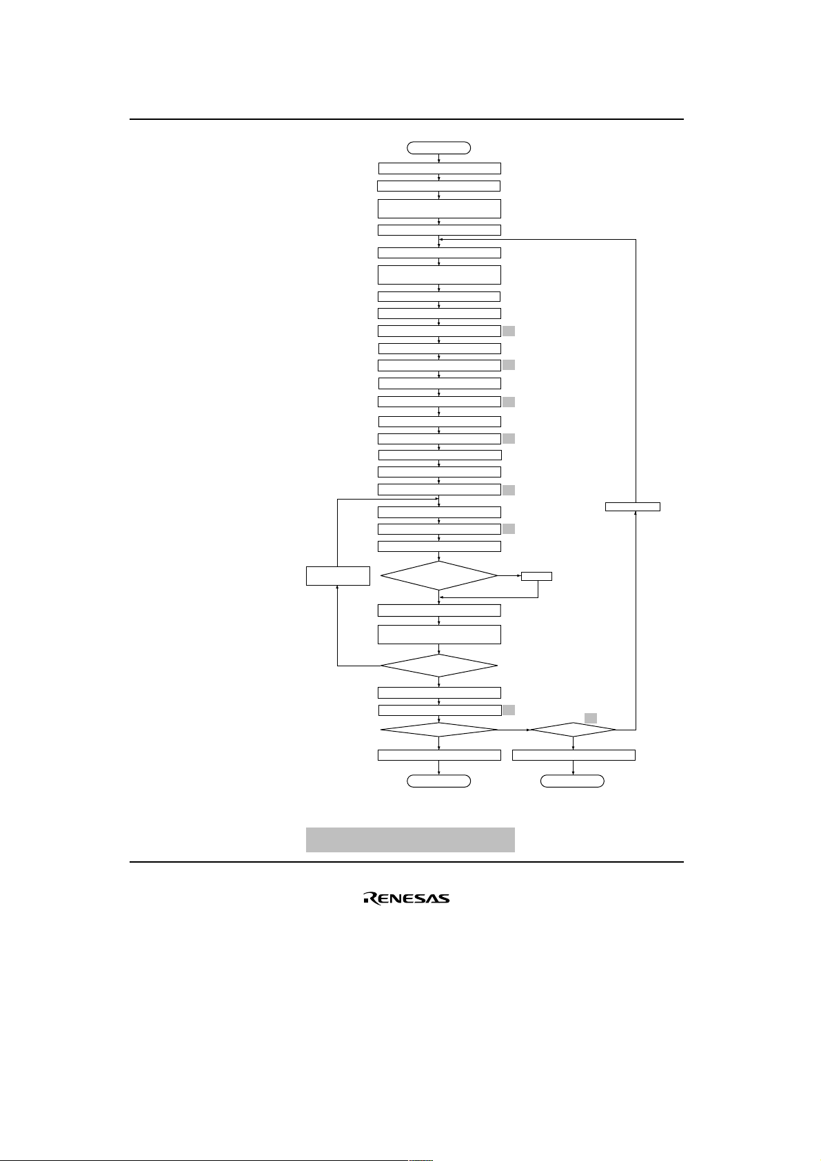
22.7.2 Program-
706
Figure amended
Verify Mode
Figure 22.13
Program/Program
Verify Flow
Verify
Increment address
NG
Start
Set SWE bit in FLMCR1
Wait 10 µs
Store 32-byte program data in
reprogram data area
n = 1
m = 0
Write 32-byte data in reprogram data area
in RAM to flash memory consecutively
Enable WDT
Set PSU1(2) bit in FLMCR1(2)
Wait 50 µs
Set P1(2) bit in FLMCR1(2)
Wait 200 µs
Clear P1(2) bit in FLMCR1(2)
Wait 10 µs
Clear PSU1(2) bit in FLMCR1(2)
Wait 10 µs
Disable WDT
Set PV1(2) bit in FLMCR1(2)
Wait 4 µs
Dummy write of H'FF to verify address
Wait 2 µs
Read verify data
3
Program data = verify data?
OK
Reprogram data computation
Transfer reprogram data to reprogram
data area
End of 32-byte
data verification?
OK
Clear PV1(2) bit in FLMCR1(2)
Wait 4 µs
flag = 0?
OK
Clear SWE bit in FLMCR1
*
5
*
4
*
1
*
5
*
Start of programming
5
*
End of programming
5
*
5
*
5
*
5
*
2
*
m = 1
NG
3
*
4
*
5
*
NG NG
Clear SWE bit in FLMCR1
n ≥ 1000
5
*
*5
OK
n ← n + 1
End of programming
Note *5 added.
*5 Make sure to set the wait times and repetitions as specified.
Programming may not complete correctly if values other than
the specified ones are used.
Programming failure
Page 13
Section Page Description
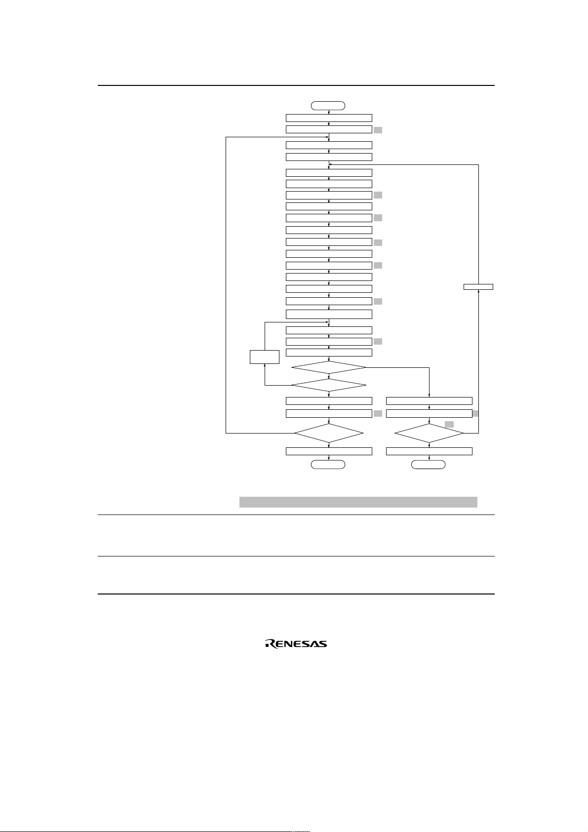
22.7.4 Erase-Verify
713
Figure amended
Mode
Figure 22.14
Erase/Erase-Verify
Flowchart
Increment
address
Notes: *1 Preprogramming (setting erase block data to all “0”) is not necessary.
*2 Verify data is read in 32-bit (longword) units.
*3 Set only one bit in EBR1(2). More than one bit cannot be set.
*4 Erasing is performed in block units. To erase a number of blocks, each block must be erased in turn.
*5 Make sure to set the wait times and repetitions as specified. Erasing may not complete correctly if values other
than the specified ones are used.
*1
Start
Set SWE bit in FLMCR1
Wait 10 µs
n = 1
Set EBR1(2)
Enable WDT
Set ESU1(2) bit in FLMCR1(2)
Wait 200 µs
Set E1(2) bit in FLMCR1(2)
Wait 5 ms
Clear E1(2) bit in FLMCR1(2)
Wait 10 µs
Clear ESU1(2) bit in FLMCR1(2)
Wait 10 µs
Disable WDT
Set EV1(2) bit in FLMCR1(2)
Wait 20 µs
Set block start address to verify address
H'FF dummy write to verify address
Wait 2 µs
Read verify data
Verify data = all "1"?
NG
Clear EV1(2) bit in FLMCR1(2)
*4
NG
Clear SWE bit in FLMCR1
OK
Last address of block?
OK
Wait 5 µs
End of
erasing of all erase
blocks?
OK
End of erasing
*5
*3
*5
Start erase
*5
Halt erase
*5
*5
*5
*5
*2
NG
Clear EV1(2) bit in FLMCR1(2)
*5 *5
Wait 5 µs
*5
n ≥ 60?
Clear SWE bit in FLMCR1
OK
Erase failure
n ← n + 1
NG
24.4.2 Canceling the
Standby Mode
25. Electrical
Characteristics (5V,
33.3 MHz Version)
747
—
Cancellation by a Manual Reset deleted
Deleted
Page 14
Section Page Description
25.2 DC
Characteristics
751 Note amended
*2 5 mA in the A mask version, except for F-ZTAT products.
Table 25.2 DC
Characteristics
25.3.2 Control
Signal Timing
Table 25.5 Control
Signal Timing
754 Note amended
Note: * The RES, MRES, NMI, BREQ, and IRQ7–IRQ0 signals are
asynchronous inputs, but when thesetup times shown here
are provided, the signals are considered to have produced
changes at clock rise (for RES, MRES, BREQ) or clock fall
(for NMI and IRQ7–IRQ0). If the setup times are not
provided, recognition is delayed until the next clock rise or
fall.
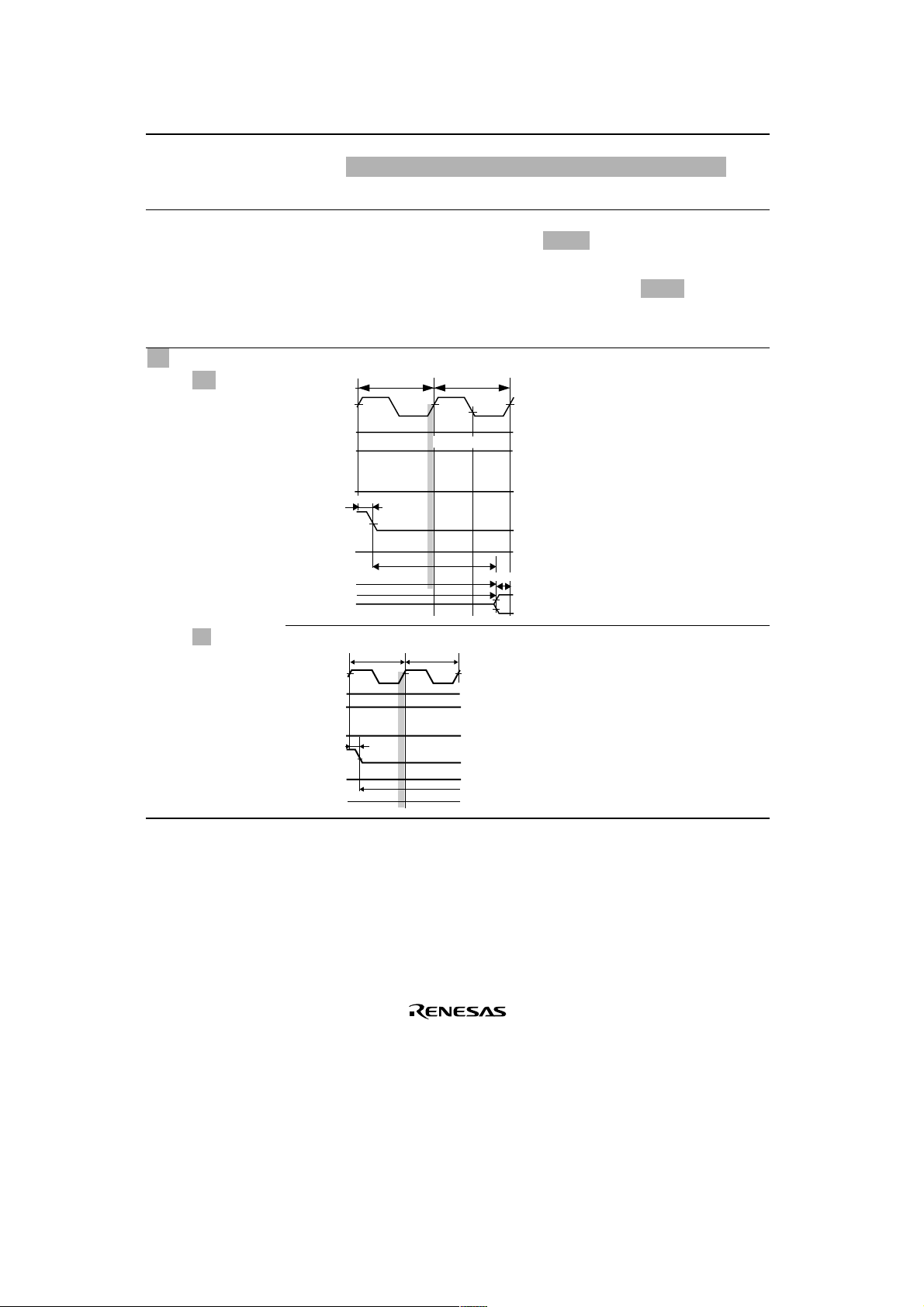
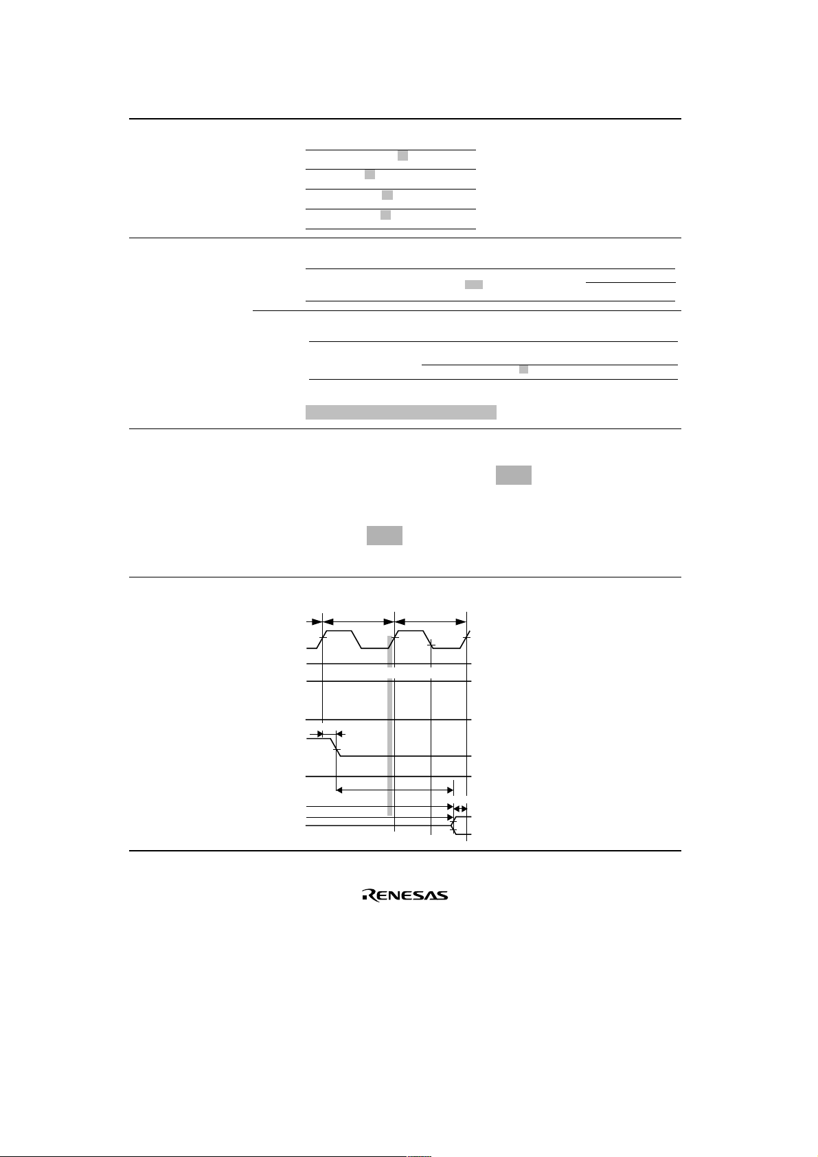
25.3.3 Bus Timing
Figure 25.12 DRAM
763 Figure amended
Tcw1 Tc2
Cycle (Normal Mode,
1 Wait, TPC=0,
RCD=0)
Column address
t
CASD1
t
CAC
t
t
RAC
t
AA
RDS
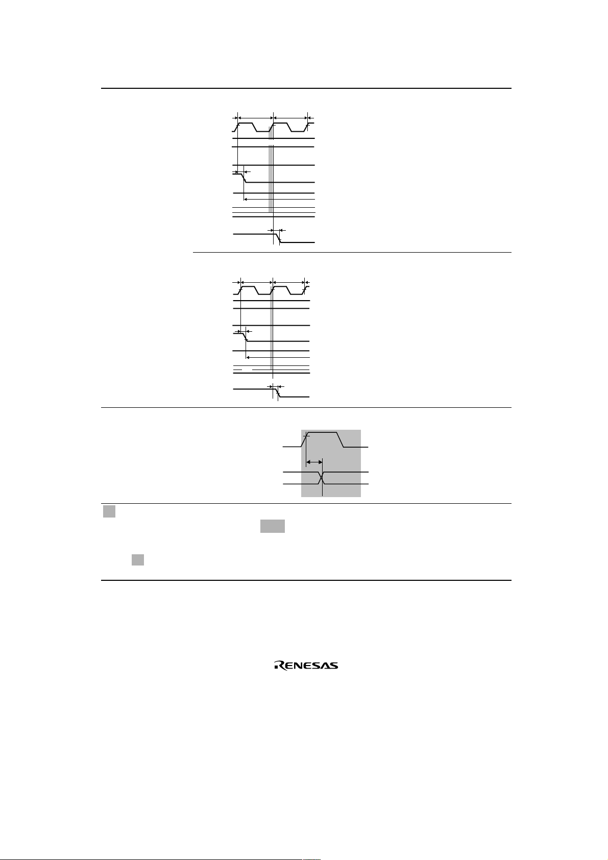
Figure 25.13 DRAM
Cycle (Normal Mode,
2 Waits, TPC=1,
RCD=1)
764 Figure amended
Tcw1 Tcw2
Column address
t
CASD1
t
CAC
t
AA
Page 15
Section Page Description
25.3.3 Bus Timing
Figure 25.14 DRAM
764 Figure amended
Tcw1 Tcw2
Cycle (Normal Mode,
3 Waits, TPC=1,
RCD=1)
t
CASD1
t
CAC
t
AA
Column
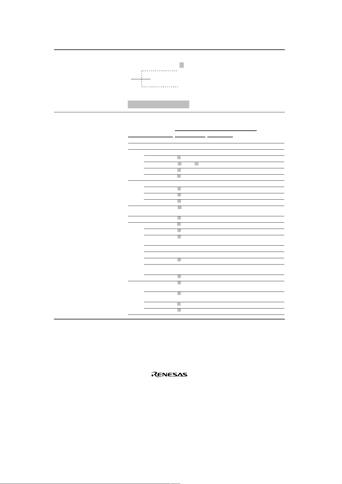
25.3.5 Multifunction
Timer Pulse Unit
Timing
Figure 25.23 MTU
I/O Timing
Figure 25.24 MTU
Clock Input Timing
25.3.11 Measuring
Conditions for AC
Characteristics
Figure 25.33 Output
Load Circuit
770 Figure amended
t
TOCD
770 Figure amended
t
TCKS
778
Title amended
Output Load Circuit
Page 16
Section Page Description
25.4 A/D Converter
779
Table amended
Characteristics
Table 25.16 A/D
Converter Timing (A
mask)
Non-linearity error
Offset error
Full scale error
Quantize error
*
*
*
*
26.2 DC
Characteristics
Table 26.2 DC
Characteristics
26.3.2 Control
Signal Timing
Table 26.5 Control
Signal Timing
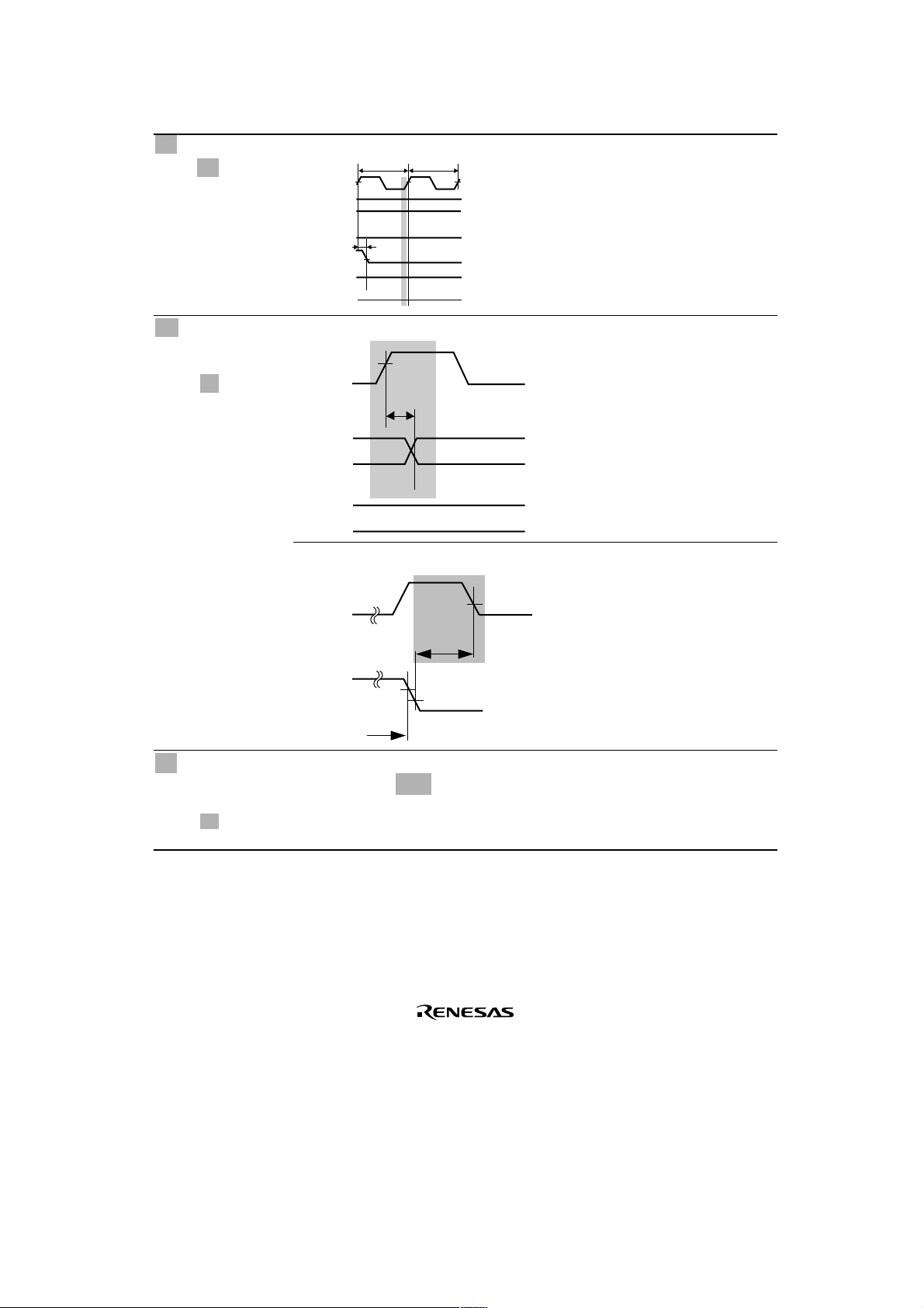
26.3.3 Bus Timing
Figure 26.12 DRAM
Cycle (Normal Mode,
1 Wait, TPC = 0,
RCD = 0)
782
783
786
795
Table amended
Schmitt
trigger input
voltage
PA2, PA5, PA6–
PA9,
PE0–PE15
–
+
V
VCC×
0.07
——
– V
T
T
+
V
VT
≥ VCC× 0.9V (min)
VT– ≤ VCC× 0.2V (max)
Table amended
Analog
supply
current
*3 2 mA in the A mask version of MASK products.
AI
CC
AI
ref
— 48
— 0.5 1
*
mA f = 16.7MHz
3
mA QFP144 version only
Note amended
Notes: *1 SH7042/43 ZTAT (excluding A mask) are 3.2V.
*2 The RES, MRES, NMI, BREQ, and IRQ7–IRQ0 signals
are asynchronous inputs, but when the setup times
shown here are provided, the signals are considered to
have produced changes at clock rise (for RES, MRES,
BREQ) or clock fall (for NMI and IRQ7–IRQ0). If the
setup times are not provided, recognition is delayed until
the next clock rise or fall.
Figure amended
Tcw1 Tc2
Column address
t
CASD1
t
CAC
t
AA
t
RAC
t
RDS
Page 17
Section Page Description
26.3.3 Bus Timing
Figure 26.13 DRAM
796
Figure amended
Tcw1 Tcw2
Cycle (Normal Mode,
2 Waits, TPC = 1,
RCD = 1)
t
CASD1
t
RAC
Column address
t
CAC
t
AA
t
CASD1
Figure 26.14 DRAM
Cycle (Normal Mode,
3 Waits, TPC = 1,
RCD = 1)
26.3.5 Multifunction
Timer Pulse Unit
Timing
Figure 26.23 MTU
I/O Timing
26.3.11
Measurement
Conditions for AC
Characteristics
Figure 26.33 Output
Load Circuit
796
802
810
Figure amended
Tcw1 Tcw2
Column address
t
CASD1
t
CAC
t
AA
t
RAC
t
CASD1
Figure amended
CK
Output
compare output
Title amended
Output Load Circuit
t
TOCD
Page 18
Section Page Description
Appendix B Block
844
Note added
Diagrams
Figure B.19
On-chip flash memory
PB4/IRQ2/POE2/
CASH,PB3/IRQ1/
POE1/CASL
Block Diagram
(F-ZTAT Version)
Note: * Only when n = 4.
*
A17
Appendix C Pin
States
Table C.1 Pin
Modes During Reset,
Power-Down, and
Bus Right Release
Modes (144 Pin)
865
Table amended
Pin modes
Pin Function Reset Power-Down
Class Pin Name Power-OnManual Standby Sleep Release Right Release
1
Clock CK O O H
*
System RES IIIII I
control
MRES Z
WDTOVF O
BREQ Z
BACK Z
4
*
IZII Z
3
*
4
*
4
*
3
*
O
OOO O
IZII I
OZOL L
Interrupt NMI I I I I I I
4
IRQ0–IRQ7 Z
IRQOUT (PD30) Z
IRQOUT (PE15) Z
Address
A0–A21 O
bus
Data bus D0–D31 Z
Bus WAIT Z
control
RD/WR, RAS Z
CASH, CASL,
CASLH, CASLL
*
IZII Z
4
*
OH
4
*
OZHO Z
2
*
OZOZ Z
4
*
I/O Z I/O Z Z
4
*
IZIZ Z
4
*
OOOZ Z
4
*
Z
OOOZ Z
1
*
RD HOZOZ Z
CS0, CS1 HOZOZ Z
4
CS2, CS3 Z
WRHH, WRHL,
WRH, WRL
AH Z
DMAC DACK0, DACK1
(PD26, PD27)
DACK0, DACK1
(PE14, PE15)
DRAK0, DRAK1 Z
DREQ0, DREQ1 Z
*
OZOZ Z
HOZOZ Z
4
*
OZOZ Z
4
*
Z
OO
4
*
Z
OZOO Z
4
*
OO
4
*
IZII Z
1
*
1
*
Bus Right Standby in Bus
OO O
1
HO H
OO O
OO O
*
1
*
1
*
Page 19

Section Page Description
Appendix C Pin
866
Table amended
States
Table C.1 Pin
Modes During Reset,
Power-Down, and
Bus Right Release
Modes (144 Pin)
(cont)
Pin Function Reset Power-Down
Class Pin Name Power-OnManual Standby Sleep Release Right Release
MTU TIOC0A–TIOC0D,
TIOC1A–TIOC1D,
TIOC2A–TIOC2D,
TIOC3A, TIOC3C
TIOC3B,TIOC3D,
TIOC4A–TIOC4D
TCLKA–TCLKD Z
Port
POE0–POE3 Z
control
SCI SCK0–SCK1 Z
TXD0–TCD1 Z
RXD0–RXD1 Z
A/D ADTRG Z
converter
AN0–AN7 Z I Z I I Z
I/O Port PA0–PA23 Z
PB0–PB9
PC0–PC15
PD0–PD31
PE0–PE8,PE10
PE9,PE11–PE15 Z
PF0–PF17 Z I Z I I Z
Notes: 1. There are instances where bus right release and transition to software standby mode
occur simultaneously due to the timing between BREQ and internal operations. In such
cases, standby mode results, but the standby state may be different.
The initial pin states depend on the mode. See section 18, Pin Function Controller
(PFC), for details.
2. I: Input, O: Output, H: High-level output, L: Low-level output, Z: High impedance,
K: Input pin with high impedance, output pin mode maintained.
*1 If the standby control register port high-impedance bits are set to 1, output pins become
high impedance.
*2 A21–A18 will become input ports after power-on reset.
*3 Input in the SH7044/SH7045 F-ZTAT version.
*4 General use I/O ports PAn, PBn, PCn, PDn, and PEn, as well as pins multiplexed with
them, are unstable during the RES setup time (t
goes to low level.
Pin modes
Bus Right Standby in Bus
4
*
Z
I/O K
4
*
Z
I/O Z I/O I/O Z
4
*
IZII Z
4
*
IZII Z
4
*
I/O Z I/O I/O Z
4
*
OO
4
*
IZII Z
4
*
IZII Z
4
*
I/O K
4
*
I/O Z K I/O Z
1
*
I/O I/O K
1
*
OO O
1
*
K I/O K
) immediately after the RES pin
RESS
1
*
1
*
1
*
Page 20
Section Page Description
Appendix C Pin
867
Table amended
States
Table C.2 Pin
Modes During Reset,
Power-Down, and
Bus Right Release
Modes (112 Pin,
120 Pin)
Pin Function Reset Power-Down
Class Pin Name Power-OnManual Standby Sleep Release Right Release
Clock CK O O H
System RES IIIII I
control
MRES Z
WDTOVF O
BREQ Z
BACK Z
Interrupt NMI I I I I I I
IRQ0–IRQ7 Z
IRQOUT Z
Address
A0–A21 O
bus
Data bus D0–D31 Z
Bus WAIT Z
control
RDWR, RAS Z
CASH, CASL Z
RD HOZOZ Z
CS0, CS1 HOZOZ Z
CS2, CS3 Z
WRH, WRL HOZOZ Z
AH Z
DMAC DACK0–DACK1 Z
DRAK0–DRAK1 Z
DREQ0–DREQ1 Z
MTU TIOC0A–TIOC0D,
TIOC1A–TIOC1D,
TIOC2A–TIOC2D,
TIOC3A, TIOC3C
TIOC3B,TIOC3D,
TIOC4A–TIOC4D
TCLKA–TCLKD Z
Pin modes
Bus Right Standby in Bus
1
*
OO O
4
*
IZII Z
3
*
4
*
4
*
4
*
4
*
*
4
*
4
*
4
*
4
*
4
*
4
*
4
*
4
*
4
*
4
*
Z
4
*
Z
4
*
3
*
O
OOO O
IZII I
OZOL L
IZII Z
OZHO Z
2
OZOZ Z
I/O Z I/O Z Z
IZIZ Z
OOOZ Z
OOOZ Z
OZOZ Z
OZOZ Z
OZOO Z
OZOO Z
IZII Z
1
I/O K
*
I/O I/O K
I/O Z I/O I/O Z
IZII Z
1
*
Page 21
Section Page Description
Appendix C Pin
868
Table amended
States
Table C.2 Pin
Modes During Reset,
Power-Down, and
Bus Right Release
Modes (112 Pin,
120 Pin) (cont)
Pin Function Reset Power-Down
Class Pin Name Power-OnManual Standby Sleep Release Right Release
Port
POE0–POE3 Z
control
SCI SCK0–SCK1 Z
TXD0–TCD1 Z
RXD0–RXD1 Z
A/D
ADTRG Z
converter
control
AN0–AN7 Z I Z I I Z
I/O Port PA0–PA15 Z
PB0–PB9
PC0–PC15
PD0–PD15
PE0–PE8–PE10
PE9,PE11–PE15 Z
PF0–PF7 Z I Z I I Z
Notes: 1. There are instances where bus right release and transition to software standby mode
occur simultaneously due to the timing between BREQ and internal operations. In such
cases, standby mode results, but the standby state may be different.
The initial pin states depend on the mode. See section 18, Pin Function Controller
(PFC), for details.
2. I: Input, O: Output, H: High-level output, L: Low-level output, Z: High impedance,
K: Input pin with high impedance, output pin mode maintained.
*1 If the standby control register port high-impedance bits are set to 1, output pins become
high impedance.
*2A21–A18 will become input ports after power-on reset.
*3 Input in the SH7044/SH7045 F-ZTAT version.
*4 General use I/O ports PAn, PBn, PCn, PDn, and PEn, as well as pins multiplexed with
them, are unstable during the RES setup time (t
goes to low level.
Pin modes
Bus Right Standby in Bus
4
*
IZII Z
4
*
I/O Z I/O I/O Z
4
*
OO
4
*
IZII Z
4
*
IZII Z
4
*
I/O K
4
*
I/O Z K I/O Z
1
*
OO O
1
*
K I/O K
) immediately after the RES pin
RESS
1
*
1
*
Page 22

Section Page Description
Appendix E Product
Code Lineup
Table E.1 SH7040,
SH7041, SH7042,
876,
877
Table amended
Product
Type
SH7040A Mask ROM
verion
SH7043, SH7044,
and SH7045 Product
Lineup
ROM less
verion
SH7041A Mask ROM
verion
ROM less
verion
SH7042 Mask ROM
verion
Z-TAT
version
SH7042A Mask ROM
verion
Product
Type
SH7042A Z-TAT
version
SH7043 Mask ROM
version
Z-TAT
version
SH7043A Mask ROM
version
Z-TAT
version
SH7044 Mask ROM
version
F-ZTAT
version
SH7045 Mask ROM
version
F-ZTAT
version
(***) is the ROM code.
NoteS: 1. Package with Copper used as the lead material.
2. *** in the Order Model No. is the ROM code, consisting of a letter and a two-digit
number (ex. E00). The letter indicates the voltage and frequency, as shown below.
• E, F, G, H: 5.0 V, 28 MHz
• P, Q, R: 3.3 V, 16 MHz
Mask
Product Code Mark Code Package Order Model No.*
Version
A MASK HD6437040AF28
HD6437040AVF16
HD6437040AVX16
HD6437040ACF28
HD6437040AVCF16
A MASK HD6417040AF28
HD6417040AVF16
HD6417040AVX16
HD6417040ACF28
HD6417040AVCF16
A MASK HD6437041AF28
HD6437041AVF16
HD6437041ACF28
HD6437041AVCF16
A MASK HD6417041AF28
HD6417041AVF16
HD6417041ACF28
HD6417041AVCF16
– HD6437042F28
HD6437042VF16
– HD6477042F28
HD6477042VF16
A MASK HD6437042AF28
HD6437042AVF16
HD6437042AVX16
HD6437042ACF28
HD6437042AVCF16
Mask
Product Code Mark Code Package Order Model No.*
Version
A MASK HD6477042AF28
HD6477042AVF16
HD6477042AVX16
HD6477042ACF28
HD6477042AVCF16
– HD6437043F28
HD6437043VF16
– HD6477043F28
HD6477043VF16
A MASK HD6437043AF28
HD6437043AVF16
HD6437043ACF28
HD6437043AVCF16
A MASK HD6477043AF28
HD6477043AVF16
HD6477043ACF28
HD6477043AVCF16
A MASK HD6437044F28 HD6437044(***)F28 QFP2020-112 HD6437044***F
HD64F7044F28 HD64F7044F28 QFP2020-112 HD64F7044F28
A MASK HD6437045F28 HD6437045(***)F28 QFP2020-144 HD6437045***F
HD64F7045F28 HD64F7045F28 QFP2020-144 HD64F7045F28
HD6437040A (***)F28
HD6437040A(***)VF16
HD6437040A(***)VX16
HD6437040A(***)CF28
HD6437040A(***)VCF16
HD6417040AF28
HD6417040AVF16
HD6417040AVX16
HD6417040ACF28
HD6417040AVCF16
HD6437041A(***)F28
HD6437041A(***)VF16
HD6437041A(***)CF28
HD6437041A(***)VCF16
HD6417041AF28
HD6417041AVF16
HD6417041ACF28
HD6417041AVCF16
HD6437042 (***)F28
HD6437042 (***)VF16
HD6477042F28
HD6477042VF16
HD6437042A(***)F28
HD6437042A(***)VF16
HD6437042A(***)VX16
HD6437042A(***)CF28
HD6437042A(***)VCF16
HD6477042AF28
HD6477042AVF16
HD6477042AVX16
HD6477042ACF28
HD6477042AVCF16
HD6437043(***)F28
HD6437043(***)VF16
HD6477043F28
HD6477043VF16
HD6437043A(***)F28
HD6437043A(***)VF16
HD6437043A(***)CF28
HD6437043A(***)VCF16
HD6477043AF28
HD6477043AVF16
HD6477043ACF28
HD6477043AVCF16
QFP2020-112
QFP2020-112
TQFP1414-120
QFP2020-112Cu*
QFP2020-112Cu*
QFP2020-112
QFP2020-112
TQFP1414-120
QFP2020-112Cu*
QFP2020-112Cu*
QFP2020-144
QFP2020-144
QFP2020-144Cu*
QFP2020-144Cu*
QFP2020-144
QFP2020-144
QFP2020-144Cu*
QFP2020-144Cu*
QFP2020-112
QFP2020-112
QFP2020-112
QFP2020-112
QFP2020-112
QFP2020-112
TQFP1414-120
QFP2020-112Cu*
QFP2020-112Cu*
QFP2020-112
QFP2020-112
TQFP1414-120
QFP2020-112Cu*
QFP2020-112Cu*
QFP2020-144
QFP2020-144
QFP2020-144
QFP2020-144
QFP2020-144
QFP2020-144
QFP2020-144Cu*
QFP2020-144Cu*
QFP2020-144
QFP2020-144
QFP2020-144Cu*
QFP2020-144Cu*
HD6437040A***F
HD6437040A***F
HD6437040A***X
1
HD6437040A***CF
1
HD6437040A***CF
HD6417040AF28
HD6417040AVF16
HD6417040AVX16
1
HD6417040ACF28
1
HD6417040AVCF16
HD6437041A***F
HD6437041A***F
1
HD6437041A***CF
1
HD6437041A***CF
HD6417041AF28
HD6417041AVF16
1
HD6417041ACF28
1
HD6417041AVCF16
HD6437042***F
HD6437042***F
HD6477042F28
HD6477042VF16
HD6437042A***F
HD6437042A***F
HD6437042A***X
1
HD6437042A***CF
1
HD6437042A***CF
HD6477042AF28
HD6477042AVF16
HD6477042AVX16
1
HD6477042ACF28
1
HD6477042AVCF16
HD6437043***F
HD6437043***F
HD6477043F28
HD6477043VF16
HD6437043A***F
HD6437043A***F
1
HD6437043A***CF
1
HD6437043A***CF
HD6477043AF28
HD6477043AVF16
1
HD6477043ACF28
1
HD6477043AVCF16
2
2
Page 23

Contents
Section 1 SH7040 Series Overview............................................................................. 1
1.1 SH7040 Series Overview................................................................................................... 1
1.1.1 SH7040 Series Features........................................................................................ 1
1.2 Block Diagram................................................................................................................... 11
1.3 Pin Arrangement and Pin Functions.................................................................................. 13
1.3.1 Pin Arrangment..................................................................................................... 13
1.3.2 Pin Arrangement by Mode ................................................................................... 16
1.3.3 Pin Functions ........................................................................................................ 37
1.4 The F-ZTAT Version Onboard Programming................................................................... 42
Section 2 CPU..................................................................................................................... 45
2.1 Register Configuration....................................................................................................... 45
2.1.1 General Registers (Rn) ......................................................................................... 45
2.1.2 Control Registers .................................................................................................. 46
2.1.3 System Registers................................................................................................... 47
2.1.4 Initial Values of Registers .................................................................................... 47
2.2 Data Formats...................................................................................................................... 48
2.2.1 Data Format in Registers ...................................................................................... 48
2.2.2 Data Format in Memory....................................................................................... 48
2.2.3 Immediate Data Format........................................................................................ 48
2.3 Instruction Features ........................................................................................................... 49
2.3.1 RISC-Type Instruction Set ................................................................................... 49
2.3.2 Addressing Modes ................................................................................................ 52
2.3.3 Instruction Format ................................................................................................ 56
2.4 Instruction Set by Classification........................................................................................ 59
2.5 Processing States ............................................................................................................... 72
2.5.1 State Transitions................................................................................................... 72
2.5.2 Power-Down State................................................................................................ 74
Section 3 Operating Modes............................................................................................. 77
3.1 Operating Modes, Types, and Selection............................................................................ 77
3.2 Explanation of Operating Modes....................................................................................... 78
3.3 Pin Configuration............................................................................................................... 79
Section 4 Clock Pulse Generator (CPG)..................................................................... 81
4.1 Overview............................................................................................................................ 81
4.1.1 Block Diagram...................................................................................................... 81
4.2 Oscillator............................................................................................................................ 81
4.2.1 Connecting a Crystal Oscillator............................................................................ 81
i
Page 24

4.2.2 External Clock Input Method............................................................................... 82
4.3 Prescaler............................................................................................................................. 83
4.4 Oscillator Halt Function..................................................................................................... 83
4.5 Usage Notes....................................................................................................................... 83
4.5.1 Oscillator Usage Notes......................................................................................... 83
4.5.2 Notes on Board Design......................................................................................... 84
4.5.3 Spread Spectrum Clock Generator Usage Notes.................................................. 85
Section 5 Exception Processing..................................................................................... 87
5.1 Overview............................................................................................................................ 87
5.1.1 Types of Exception Processing and Priority......................................................... 87
5.1.2 Exception Processing Operations......................................................................... 88
5.1.3 Exception Processing Vector Table...................................................................... 89
5.2 Resets................................................................................................................................. 90
5.2.1 Power-On Reset.................................................................................................... 91
5.2.2 Manual Reset ........................................................................................................ 91
5.3 Address Errors ................................................................................................................... 92
5.3.1 Address Error Exception Processing .................................................................... 93
5.4 Interrupts............................................................................................................................ 93
5.4.1 Interrupt Priority Level......................................................................................... 94
5.4.2 Interrupt Exception Processing............................................................................. 94
5.5 Exceptions Triggered by Instructions................................................................................ 94
5.5.1 Trap Instructions................................................................................................... 95
5.5.2 Illegal Slot Instructions......................................................................................... 95
5.5.3 General Illegal Instructions................................................................................... 96
5.6 When Exception Sources Are Not Accepted..................................................................... 96
5.6.1 Immediately after a Delayed Branch Instruction.................................................. 96
5.6.2 Immediately after an Interrupt-Disabled Instruction............................................ 96
5.7 Stack Status after Exception Processing Ends................................................................... 97
5.8 Notes on Use...................................................................................................................... 98
5.8.1 Value of Stack Pointer (SP).................................................................................. 98
5.8.2 Value of Vector Base Register (VBR) ................................................................. 98
5.8.3 Address Errors Caused by Stacking of Address Error Exception Processing...... 98
Section 6 Interrupt Controller (INTC)......................................................................... 99
6.1 Overview............................................................................................................................ 99
6.1.1 Features................................................................................................................. 99
6.1.2 Block Diagram...................................................................................................... 99
6.1.3 Pin Configuration ................................................................................................. 101
6.1.4 Register Configuration ......................................................................................... 101
6.2 Interrupt Sources................................................................................................................ 102
6.2.1 NMI Interrupts...................................................................................................... 102
6.2.2 User Break Interrupt............................................................................................. 102
ii
Page 25

6.2.3 IRQ Interrupts....................................................................................................... 102
6.2.4 On-Chip Peripheral Module Interrupts................................................................. 103
6.2.5 Interrupt Exception Vectors and Priority Rankings ............................................. 103
6.3 Description of Registers..................................................................................................... 108
6.3.1 Interrupt Priority Registers A–H (IPRA–IPRH)................................................... 108
6.3.2 Interrupt Control Register (ICR) .......................................................................... 109
6.3.3 IRQ Status Register (ISR) .................................................................................... 110
6.4 Interrupt Operation............................................................................................................. 112
6.4.1 Interrupt Sequence................................................................................................ 112
6.4.2 Stack after Interrupt Exception Processing........................................................... 114
6.5 Interrupt Response Time.................................................................................................... 114
6.6 Data Transfer with Interrupt Request Signals ................................................................... 116
6.6.1 Handling DTC Activating and CPU Interrupt Sources,
but Not DMAC Activating Sources ..................................................................... 117
6.6.2 Handling DMAC Activating Sources but Not CPU Interrupt
or DTC Activating Sources .................................................................................. 118
6.6.3 Handling DTC Activating Sources but Not CPU Interrupt
or DMAC Activating Sources .............................................................................. 118
6.6.4 Treating CPU Interrupt Sources but Not DTC
or DMAC Activating Sources .............................................................................. 118
Section 7 User Break Controller (UBC)..................................................................... 119
7.1 Overview............................................................................................................................ 119
7.1.1 Features................................................................................................................. 119
7.1.2 Block Diagram...................................................................................................... 119
7.1.3 Register Configuration ......................................................................................... 120
7.2 Register Descriptions......................................................................................................... 121
7.2.1 User Break Address Register (UBAR)................................................................. 121
7.2.2 User Break Address Mask Register (UBAMR) ................................................... 122
7.2.3 User Break Bus Cycle Register (UBBR).............................................................. 123
7.3 Operation ........................................................................................................................... 126
7.3.1 Flow of the User Break Operation ....................................................................... 126
7.3.2 Break on On-Chip Memory Instruction Fetch Cycle ........................................... 128
7.3.3 Program Counter (PC) Values Saved................................................................... 128
7.4 Use Examples..................................................................................................................... 128
7.4.1 Break on CPU Instruction Fetch Cycle ................................................................ 128
7.4.2 Break on CPU Data Access Cycle........................................................................ 129
7.4.3 Break on DMA/DTC Cycle.................................................................................. 130
7.5 Cautions on Use................................................................................................................. 130
7.5.1 On-Chip Memory Instruction Fetch..................................................................... 130
7.5.2 Instruction Fetch at Branches............................................................................... 130
7.5.3 Contention between User Break and Exception Handling................................... 131
7.5.4 Break at Non-Delay Branch Instruction Jump Destination.................................. 131
iii
Page 26

Section 8 Data Transfer Controller (DTC)................................................................. 133
8.1 Overview............................................................................................................................ 133
8.1.1 Features................................................................................................................. 133
8.1.2 Block Diagram...................................................................................................... 134
8.1.3 Register Configuration ......................................................................................... 135
8.2 Register Description .......................................................................................................... 135
8.2.1 DTC Mode Register (DTMR) .............................................................................. 135
8.2.2 DTC Source Address Register (DTSAR)............................................................. 138
8.2.3 DTC Destination Address Register (DTDAR)..................................................... 138
8.2.4 DTC Initial Address Register (DTIAR) ............................................................... 139
8.2.5 DTC Transfer Count Register A (DTCRA) ......................................................... 139
8.2.6 DTC Transfer Count Register B (DTCRB).......................................................... 140
8.2.7 DTC Enable Registers (DTER) ............................................................................ 140
8.2.8 DTC Control/Status Register (DTCSR)............................................................... 141
8.2.9 DTC Information Base Register (DTBR)............................................................. 143
8.3 Operation ........................................................................................................................... 143
8.3.1 Overview of Operation......................................................................................... 143
8.3.2 Activating Sources................................................................................................ 145
8.3.3 DTC Vector Table ................................................................................................ 145
8.3.4 Register Information Placement........................................................................... 148
8.3.5 Normal Mode........................................................................................................ 149
8.3.6 Repeat Mode......................................................................................................... 149
8.3.7 Block Transfer Mode............................................................................................ 150
8.3.8 Operation Timing ................................................................................................. 151
8.3.9 DTC Execution State Counts................................................................................ 151
8.3.10 DTC Usage Procedure .......................................................................................... 153
8.3.11 DTC Use Example................................................................................................ 153
8.4 Cautions on Use................................................................................................................. 154
Section 9 Cache Memory (CAC).................................................................................. 155
9.1 Overview............................................................................................................................ 155
9.1.1 Features................................................................................................................. 155
9.1.2 Block Diagram...................................................................................................... 156
9.1.3 Register Configuration ......................................................................................... 156
9.2 Register Explanation.......................................................................................................... 157
9.2.1 Cache Control Register (CCR)............................................................................. 157
9.3 Address Array and Data Array .......................................................................................... 158
9.3.1 Cache Address Array Read/Write Space.............................................................. 159
9.3.2 Cache Data Array Read/Write Space ................................................................... 159
9.4 Cautions on Use................................................................................................................. 160
9.4.1 Cache Initialization............................................................................................... 160
9.4.2 Forced Access to Address Array and Data Array................................................. 160
9.4.3 Cache Miss Penalty and Cache Fill Timing ......................................................... 160
iv
Page 27

9.4.4 Cache Hit after Cache Miss.................................................................................. 162
Section 10 Bus State Controller (BSC) ......................................................................... 163
10.1 Overview............................................................................................................................ 163
10.1.1 Features................................................................................................................. 163
10.1.2 Block Diagram...................................................................................................... 164
10.1.3 Pin Configuration ................................................................................................. 165
10.1.4 Register Configuration ......................................................................................... 166
10.1.5 Address Map......................................................................................................... 167
10.2 Description of Registers..................................................................................................... 169
10.2.1 Bus Control Register 1 (BCR1)............................................................................ 169
10.2.2 Bus Control Register 2 (BCR2)............................................................................ 172
10.2.3 Wait Control Register 1 (WCR1)......................................................................... 175
10.2.4 Wait Control Register 2 (WCR2)......................................................................... 177
10.2.5 DRAM Area Control Register (DCR) .................................................................. 178
10.2.6 Refresh Timer Control/Status Register (RTCSR) ................................................ 181
10.2.7 Refresh Timer Counter (RTCNT) ........................................................................ 183
10.2.8 Refresh Time Constant Register (RTCOR).......................................................... 184
10.3 Accessing Ordinary Space................................................................................................. 185
10.3.1 Basic Timing......................................................................................................... 185
10.3.2 Wait State Control ................................................................................................ 186
10.3.3 CS Assert Period Extension.................................................................................. 188
10.4 DRAM Access................................................................................................................... 189
10.4.1 DRAM Direct Connection.................................................................................... 189
10.4.2 Basic Timing......................................................................................................... 190
10.4.3 Wait State Control ................................................................................................ 191
10.4.4 Burst Operation..................................................................................................... 195
10.4.5 Refresh Timing..................................................................................................... 197
10.5 Address/Data Multiplex I/O Space Access........................................................................ 199
10.5.1 Basic Timing......................................................................................................... 199
10.5.2 Wait State Control ................................................................................................ 200
10.5.3 CS Assertion Extension ........................................................................................ 201
10.6 Waits between Access Cycles........................................................................................... 201
10.6.1 Prevention of Data Bus Conflicts......................................................................... 201
10.6.2 Simplification of Bus Cycle Start Detection ........................................................ 203
10.7 Bus Arbitration................................................................................................................... 203
10.8 Memory Connection Examples......................................................................................... 205
10.9 On-Chip Peripheral I/O Register Access........................................................................... 210
10.10 CPU Operation when Program is in External Memory..................................................... 211
Section 11 Direct Memory Access Controller (DMAC).......................................... 213
11.1 Overview............................................................................................................................ 213
11.1.1 Features................................................................................................................. 213
v
Page 28

11.1.2 Block Diagram...................................................................................................... 215
11.1.3 Pin Configuration ................................................................................................. 216
11.1.4 Register Configuration ......................................................................................... 217
11.2 Register Descriptions......................................................................................................... 218
11.2.1 DMA Source Address Registers 0–3 (SAR0–SAR3)........................................... 218
11.2.2 DMA Destination Address Registers 0–3 (DAR0–DAR3).................................. 219
11.2.3 DMA Transfer Count Registers 0–3 (DMATCR0–DMATCR3)......................... 220
11.2.4 DMA Channel Control Registers 0–3 (CHCR0–CHCR3)................................... 221
11.2.5 DMAC Operation Register (DMAOR) ................................................................ 226
11.3 Operation........................................................................................................................... 228
11.3.1 DMA Transfer Flow............................................................................................. 228
11.3.2 DMA Transfer Requests....................................................................................... 230
11.3.3 Channel Priority.................................................................................................... 232
11.3.4 DMA Transfer Types ........................................................................................... 235
11.3.5 Address Modes ..................................................................................................... 235
11.3.6 Dual Address Mode .............................................................................................. 237
11.3.7 Bus Modes ............................................................................................................ 244
11.3.8 Relationship between Request Modes and Bus Modes by DMA Transfer
Category ............................................................................................................... 245
11.3.9 Bus Mode and Channel Priority Order................................................................. 246
11.3.10 Number of Bus Cycle States and DREQ Pin Sample Timing.............................. 246
11.3.11 Source Address Reload Function ......................................................................... 263
11.3.12 DMA Transfer Ending Conditions ....................................................................... 264
11.3.13 DMAC Access from CPU .................................................................................... 265
11.4 Examples of Use................................................................................................................ 265
11.4.1 Example of DMA Transfer between On-Chip SCI and External Memory .......... 265
11.4.2 Example of DMA Transfer between External RAM and External Device
with DACK........................................................................................................... 266
11.4.3 Example of DMA Transfer between A/D Converter and On-Chip Memory
(Address Reload On) (Excluding A Mask) .......................................................... 266
11.4.4 Example of DMA Transfer between A/D Converter and Internal Memory
(Address Reload On) (A Mask)............................................................................ 268
11.4.5 Example of DMA Transfer between External Memory and SCI1 Send Side
(Indirect Address On)........................................................................................... 270
11.5 Cautions on Use................................................................................................................. 272
Section 12 Multifunction Timer Pulse Unit (MTU) .................................................. 273
12.1 Overview............................................................................................................................ 273
12.1.1 Features................................................................................................................. 273
12.1.2 Block Diagram...................................................................................................... 276
12.1.3 Pin Configuration ................................................................................................. 278
12.1.4 Register Configuration ......................................................................................... 280
12.2 MTU Register Descriptions............................................................................................... 283
vi
Page 29

12.2.1 Timer Control Register (TCR) ............................................................................. 283
12.2.2 Timer Mode Register (TMDR)............................................................................. 288
12.2.3 Timer I/O Control Register (TIOR) ..................................................................... 290
12.2.4 Timer Interrupt Enable Register (TIER)............................................................... 306
12.2.5 Timer Status Register (TSR) ................................................................................ 309
12.2.6 Timer Counters (TCNT)....................................................................................... 312
12.2.7 Timer General Register (TGR)............................................................................. 313
12.2.8 Timer Start Register (TSTR) ................................................................................ 313
12.2.9 Timer Synchro Register (TSYR).......................................................................... 314
12.2.10 Timer Output Master Enable Register (TOER).................................................... 315
12.2.11 Timer Output Control Register (TOCR)............................................................... 317
12.2.12 Timer Gate Control Register (TGCR) .................................................................. 318
12.2.13 Timer Subcounter (TCNTS)................................................................................. 320
12.2.14 Timer Dead Time Data Register (TDDR) ............................................................ 321
12.2.15 Timer Period Data Register (TCDR).................................................................... 321
12.2.16 Timer Period Buffer Register (TCBR)................................................................. 322
12.3 Bus Master Interface.......................................................................................................... 322
12.3.1 16-Bit Registers .................................................................................................... 322
12.3.2 8-Bit Registers ...................................................................................................... 323
12.4 Operation........................................................................................................................... 324
12.4.1 Overview............................................................................................................... 324
12.4.2 Basic Functions..................................................................................................... 325
12.4.3 Synchronous Operation ........................................................................................ 330
12.4.4 Buffer Operation................................................................................................... 333
12.4.5 Cascade Connection Mode................................................................................... 336
12.4.6 PWM Mode .......................................................................................................... 337
12.4.7 Phase Counting Mode........................................................................................... 341
12.4.8 Reset-Synchronized PWM Mode......................................................................... 348
12.4.9 Complementary PWM Mode ............................................................................... 352
12.5 Interrupts............................................................................................................................ 377
12.5.1 Interrupt Sources and Priority Ranking ................................................................ 377
12.5.2 DTC/DMAC Activation ....................................................................................... 379
12.5.3 A/D Converter Activation..................................................................................... 379
12.6 Operation Timing............................................................................................................... 380
12.6.1 Input/Output Timing............................................................................................. 380
12.6.2 Interrupt Signal Timing ........................................................................................ 385
12.7 Notes and Precautions........................................................................................................ 389
12.7.1 Input Clock Limitations........................................................................................ 389
12.7.2 Note on Cycle Setting........................................................................................... 389
12.7.3 Contention between TCNT Write and Clear ........................................................ 390
12.7.4 Contention between TCNT Write and Increment................................................. 391
12.7.5 Contention between Buffer Register Write and Compare Match......................... 392
12.7.6 Contention between TGR Read and Input Capture .............................................. 394
vii
Page 30

12.7.7 Contention between TGR Write and Input Capture............................................. 395
12.7.8 Contention between Buffer Register Write and Input Capture ............................ 396
12.7.9 Contention between TGR Write and Compare Match ......................................... 397
12.7.10 TCNT2 Write and Overflow/Underflow Contention in Cascade Connection ..... 397
12.7.11 Counter Value during Complementary PWM Mode Stop ................................... 399
12.7.12 Buffer Operation Setting in Complementary PWM Mode................................... 399
12.7.13 Reset Sync PWM Mode Buffer Operation and Compare Match Flag ................. 400
12.7.14 Overflow Flags in Reset Sync PWM Mode ......................................................... 402
12.7.15 Notes on Compare Match Flags in Complementary PWM Mode ....................... 405
12.7.16 Contention between Overflow/Underflow and Counter Clearing........................ 407
12.7.17 Contention between TCNT Write and Overflow/Underflow............................... 408
12.7.18 Cautions on Transition from Normal Operation or PWM Mode 1
to Reset-Synchronous PWM Mode...................................................................... 409
12.7.19 Output Level in Complementary PWM Mode and Reset-Synchronous PWM
Mode..................................................................................................................... 409
12.7.20 Cautions on Using the Chopping Function in Complementary PWM Mode
or Reset Synchronous PWM Mode (A Mask Excluded)...................................... 409
12.7.21 Cautions on Carrying Out Buffer Operation of Channel 0 in PWM Mode
(A Mask Excluded)............................................................................................... 409
12.7.22 Cautions on Restarting with Sync Clear of Another Channel
in Complementary PWM Mode (A Mask Excluded)........................................... 410
12.8 MTU Output Pin Initialization........................................................................................... 411
12.8.1 Operating Modes .................................................................................................. 411
12.8.2 Reset Start Operation............................................................................................ 411
12.8.3 Operation in Case of Re-Setting Due to Error During Operation, Etc. ................ 412
12.8.4 Overview of Initialization Procedures and Mode Transitions in Case of Error
during Operation, Etc............................................................................................ 412
12.9 Port Output Enable (POE)................................................................................................. 443
12.9.1 Features................................................................................................................. 443
12.9.2 Block Diagram...................................................................................................... 444
12.9.3 Pin Configuration ................................................................................................. 445
12.9.4 Register Configuration.......................................................................................... 445
12.10 POE Register Descriptions ................................................................................................ 446
12.10.1 Input Level Control/Status Register (ICSR)......................................................... 446
12.10.2 Output Level Control/Status Register (OCSR)..................................................... 449
12.11 Operation ........................................................................................................................... 451
12.11.1 Input Level Detection Operation .......................................................................... 451
12.11.2 Output-Level Compare Operation ........................................................................ 452
12.11.3 Release from High-Impedance State .................................................................... 452
12.11.4 POE timing ........................................................................................................... 453
12.11.5 Usage Notes.......................................................................................................... 453
Section 13 Watchdog Timer (WDT) .............................................................................. 455
viii
Page 31

13.1 Overview............................................................................................................................ 455
13.1.1 Features................................................................................................................. 455
13.1.2 Block Diagram...................................................................................................... 456
13.1.3 Pin Configuration ................................................................................................. 456
13.1.4 Register Configuration ......................................................................................... 457
13.2 Register Descriptions......................................................................................................... 457
13.2.1 Timer Counter (TCNT)......................................................................................... 457
13.2.2 Timer Control/Status Register (TCSR) ................................................................ 458
13.2.3 Reset Control/Status Register (RSTCSR) ............................................................ 460
13.2.4 Register Access..................................................................................................... 461
13.3 Operation........................................................................................................................... 462
13.3.1 Watchdog Timer Mode......................................................................................... 462
13.3.2 Interval Timer Mode............................................................................................. 464
13.3.3 Clearing the Standby Mode .................................................................................. 464
13.3.4 Timing of Setting the Overflow Flag (OVF)........................................................ 465
13.3.5 Timing of Setting the Watchdog Timer Overflow Flag (WOVF)........................ 465
13.4 Notes on Use...................................................................................................................... 466
13.4.1 TCNT Write and Increment Contention............................................................... 466
13.4.2 Changing CKS2–CKS0 Bit Values ...................................................................... 466
13.4.3 Changing between Watchdog Timer/Interval Timer Modes................................ 466
13.4.4 System Reset With WDTOVF ............................................................................. 467
13.4.5 Internal Reset with the Watchdog Timer.............................................................. 467
Section 14 Serial Communication Interface (SCI)..................................................... 469
14.1 Overview............................................................................................................................ 469
14.1.1 Features................................................................................................................. 469
14.1.2 Block Diagram...................................................................................................... 470
14.1.3 Pin Configuration ................................................................................................. 471
14.1.4 Register Configuration ......................................................................................... 471
14.2 Register Descriptions......................................................................................................... 472
14.2.1 Receive Shift Register (RSR)............................................................................... 472
14.2.2 Receive Data Register (RDR)............................................................................... 472
14.2.3 Transmit Shift Register (TSR).............................................................................. 472
14.2.4 Transmit Data Register (TDR) ............................................................................ 473
14.2.5 Serial Mode Register (SMR) ................................................................................ 473
14.2.6 Serial Control Register (SCR) .............................................................................. 476
14.2.7 Serial Status Register (SSR)................................................................................. 479
14.2.8 Bit Rate Register (BRR)....................................................................................... 483
14.3 Operation........................................................................................................................... 501
14.3.1 Overview............................................................................................................... 501
14.3.2 Operation in Asynchronous Mode........................................................................ 503
14.3.3 Multiprocessor Communication ........................................................................... 513
14.3.4 Clock Synchronous Operation.............................................................................. 521
ix
Page 32

14.4 SCI Interrupt Sources and the DMAC/DTC...................................................................... 532
14.5 Notes on Use...................................................................................................................... 533
14.5.1 TDR Write and TDRE Flags ................................................................................ 533
14.5.2 Simultaneous Multiple Receive Errors................................................................. 533
14.5.3 Break Detection and Processing........................................................................... 534
14.5.4 Sending a Break Signal......................................................................................... 534
14.5.5 Receive Error Flags and Transmitter Operation (Clock Synchronous Mode
Only)..................................................................................................................... 534
14.5.6 Receive Data Sampling Timing and Receive Margin in the Asynchronous
Mode..................................................................................................................... 534
14.5.7 Constraints on DMAC/DTC Use.......................................................................... 536
14.5.8 Cautions for Clock Synchronous External Clock Mode....................................... 536
14.5.9 Caution for Clock Synchronous Internal Clock Mode......................................... 536
Section 15 High Speed A/D Converter (Excluding A Mask)................................. 537
15.1 Overview............................................................................................................................ 537
15.1.1 Features................................................................................................................. 537
15.1.2 Block Diagram...................................................................................................... 538
15.1.3 Pin Configuration ................................................................................................. 538
15.1.4 Register Configuration ......................................................................................... 539
15.2 Register Descriptions......................................................................................................... 540
15.2.1 A/D Data Registers A–H (ADDRA–ADDRH) .................................................... 540
15.2.2 A/D Control/Status Register (ADCSR)................................................................ 541
15.2.3 A/D Control Register (ADCR)............................................................................. 544
15.3 Bus Master Interface.......................................................................................................... 545
15.4 Operation........................................................................................................................... 548
15.4.1 Select-Single Mode............................................................................................... 548
15.4.2 Select-Scan Mode................................................................................................. 549
15.4.3 Group-Single Mode .............................................................................................. 550
15.4.4 Group-Scan Mode................................................................................................. 551
15.4.5 Buffer Operation................................................................................................... 552
15.4.6 Simultaneous Sampling Operation....................................................................... 555
15.4.7 Conversion Start Modes ....................................................................................... 557
15.4.8 Conversion Start by External Input ...................................................................... 560
15.4.9 A/D Conversion Time........................................................................................... 561
15.5 Interrupts............................................................................................................................ 562
15.6 Notes on Use...................................................................................................................... 563
Section 16 Mid-Speed A/D Converter (A Mask)....................................................... 567
16.1 Overview............................................................................................................................ 567
16.1.1 Features................................................................................................................. 567
16.1.2 Block Diagram...................................................................................................... 568
16.1.3 Pin Configuration ................................................................................................. 569
x
Page 33

16.1.4 Register Configuration ......................................................................................... 570
16.2 Register Descriptions......................................................................................................... 571
16.2.1 A/D Data Register A–D (ADDRA0–ADDRD0, ADDRA1–ADDRD1) ............ 571
16.2.2 A/D Control/Status Register (ADCSR0, ADCSR1)............................................. 572
16.2.3 A/D Control Register (ADCR0, ADCR1)............................................................ 574
16.3 Interface with CPU............................................................................................................ 575
16.4 Operation........................................................................................................................... 576
16.4.1 Single Mode (SCAN=0)....................................................................................... 576
16.4.2 Scan Mode (SCAN=1) ......................................................................................... 578
16.4.3 Input Sampling and A/D Conversion Time.......................................................... 580
16.4.4 External Trigger Input Timing ............................................................................. 581
16.5 Interrupt and DMA, DTC Transfer Requests.................................................................... 582
16.6 A/D Conversion Precision Definitions.............................................................................. 583
16.7 Usage Notes....................................................................................................................... 584
16.7.1 Analog Voltage Settings....................................................................................... 584
16.7.2 Handling of Analog Input Pins............................................................................. 584
Section 17 Compare Match Timer (CMT) ................................................................... 587
17.1 Overview............................................................................................................................ 587
17.1.1 Features................................................................................................................. 587
17.1.2 Block Diagram...................................................................................................... 587
17.1.3 Register Configuration ......................................................................................... 589
17.2 Register Descriptions......................................................................................................... 590
17.2.1 Compare Match Timer Start Register (CMSTR) ................................................. 590
17.2.2 Compare Match Timer Control/Status Register (CMCSR).................................. 591
17.2.3 Compare Match Timer Counter (CMCNT).......................................................... 592
17.2.4 Compare Match Timer Constant Register (CMCOR).......................................... 593
17.3 Operation........................................................................................................................... 593
17.3.1 Period Count Operation ........................................................................................ 593
17.3.2 CMCNT Count Timing......................................................................................... 594
17.4 Interrupts............................................................................................................................ 594
17.4.1 Interrupt Sources and DTC Activation................................................................. 594
17.4.2 Compare Match Flag Set Timing ......................................................................... 594
17.4.3 Compare Match Flag Clear Timing...................................................................... 595
17.5 Notes on Use...................................................................................................................... 596
17.5.1 Contention between CMCNT Write and Compare Match................................... 596
17.5.2 Contention between CMCNT Word Write and Incrementation........................... 597
17.5.3 Contention between CMCNT Byte Write and Incrementation ............................ 598
Section 18 Pin Function Controller................................................................................. 599
18.1 Overview............................................................................................................................ 599
18.2 Register Configuration....................................................................................................... 607
18.3 Register Descriptions......................................................................................................... 608
xi
Page 34

18.3.1 Port A I/O Register H (PAIORH)......................................................................... 608
18.3.2 Port A I/O Register L (PAIORL) ......................................................................... 609
18.3.3 Port A Control Register H (PACRH) ................................................................... 609
18.3.4 Port A Control Registers L1, L2 (PACRL1 and PACRL2) ................................. 612
18.3.5 Port B I/O Register (PBIOR)................................................................................ 617
18.3.6 Port B Control Registers (PBCR1 and PBCR2)................................................... 618
18.3.7 Port C I/O Register (PCIOR)................................................................................ 622
18.3.8 Port C Control Register (PCCR)........................................................................... 623
18.3.9 Port D I/O Register H (PDIORH)......................................................................... 626
18.3.10 Port D I/O Register L (PDIORL) ......................................................................... 627
18.3.11 Port D Control Registers H1, H2 (PDCRH1 and PDCRH2)................................ 627
18.3.12 Port D Control Register L (PDCRL) .................................................................... 634
18.3.13 Port E I/O Register (PEIOR) ................................................................................ 638
18.3.14 Port E Control Registers 1, 2 (PECR1 and PECR2)............................................. 638
18.3.15 IRQOUT Function Control Register (IFCR)........................................................ 643
18.4 Cautions on Use................................................................................................................. 645
Section 19 I/O Ports (I/O).................................................................................................. 647
19.1 Overview............................................................................................................................ 647
19.2 Port A................................................................................................................................. 647
19.2.1 Register Configuration ......................................................................................... 650
19.2.2 Port A Data Register H (PADRH)........................................................................ 650
19.2.3 Port A Data Register L (PADRL)......................................................................... 651
19.3 Port B................................................................................................................................. 652
19.3.1 Register Configuration ......................................................................................... 652
19.3.2 Port B Data Register (PBDR)............................................................................... 653
19.4 Port C................................................................................................................................. 654
19.4.1 Register Configuration ......................................................................................... 654
19.4.2 Port C Data Register (PCDR)............................................................................... 655
19.5 Port D................................................................................................................................. 656
19.5.1 Register Configuration ......................................................................................... 658
19.5.2 Port D Data Register H (PDDRH)........................................................................ 659
19.5.3 Port D Data Register L (PDDRL)......................................................................... 660
19.6 Port E................................................................................................................................. 661
19.6.1 Register Configuration ......................................................................................... 661
19.6.2 Port E Data Register (PEDR) ............................................................................... 662
19.7 Port F................................................................................................................................. 663
19.7.1 Register Configuration ......................................................................................... 663
19.7.2 Port F Data Register (PFDR)................................................................................ 663
Section 20 64/128/256kB Mask ROM........................................................................... 665
20.1 Overview............................................................................................................................ 665
xii
Page 35

Section 21 128kB PROM................................................................................................... 669
21.1 Overview............................................................................................................................ 669
21.2 PROM Mode...................................................................................................................... 670
21.2.1 PROM Mode Settings........................................................................................... 670
21.2.2 Socket Adapter Pin Correspondence and Memory Map ...................................... 670
21.3 PROM Programming......................................................................................................... 674
21.3.1 Programming Mode Selection .............................................................................. 674
21.3.2 Write/Verify and Electrical Characteristics.......................................................... 675
21.3.3 Cautions on Writing ............................................................................................. 679
21.3.4 Post-Write Reliability........................................................................................... 680
Section 22 256kB Flash Memory (F-ZTAT)............................................................... 681
22.1 Features.............................................................................................................................. 681
22.2 Overview............................................................................................................................ 682
22.2.1 Block Diagram...................................................................................................... 682
22.2.2 Mode Transition Diagram..................................................................................... 683
22.2.3 Onboard Program Mode....................................................................................... 684
22.2.4 Flash Memory Emulation in RAM....................................................................... 686
22.2.5 Differences between Boot Mode and User Program Mode.................................. 687
22.2.6 Block Configuration ............................................................................................. 688
22.3 Pin Configuration............................................................................................................... 689
22.4 Register Configuration....................................................................................................... 689
22.5 Description of Registers..................................................................................................... 690
22.5.1 Flash Memory Control Register 1 (FLMCR1)..................................................... 690
22.5.2 Flash Memory Control Register 2 (FLMCR2)..................................................... 692
22.5.3 Erase Block Register 1 (EBR1) ............................................................................ 695
22.5.4 Erase Block Register 2 (EBR2) ............................................................................ 695
22.5.5 RAM Emulation Register (RAMER) ................................................................... 696
22.6 On-Board Programming Mode.......................................................................................... 698
22.6.1 Boot Mode ............................................................................................................ 699
22.6.2 User Program Mode ............................................................................................. 703
22.7 Programming/Erasing Flash Memory................................................................................ 704
22.7.1 Program Mode (n = 1 for Addresses H'0000–H'1FFFF,
n = 2 for Addresses H'20000–H'3FFFF)............................................................... 704
22.7.2 Program-Verify Mode (n = 1 for Addresses H'0000–H'1FFFF,
n = 2 for Addresses H'20000–H'3FFFF)............................................................... 705
22.7.3 Erase Mode (n = 1 for Addresses H'0000–H'1FFFF,
n = 2 for Addresses H'20000–H'3FFFF)............................................................... 711
22.7.4 Erase-Verify Mode (n = 1 for Addresses H'00000–H'1FFFF,
n = 2 for Addresses H'20000–H'3FFFF)............................................................... 712
22.8 Protection........................................................................................................................... 718
22.8.1 Hardware Protection............................................................................................. 718
22.8.2 Software Protection .............................................................................................. 719
xiii
Page 36

22.8.3 Error Protection .................................................................................................... 720
22.9 Flash Memory Emulation in RAM.................................................................................... 722
22.10 Note on Flash Memory Programming/Erasing.................................................................. 724
22.11 Flash Memory Programmer Mode..................................................................................... 724
22.11.1 Socket Adapter Pin Correspondence Diagrams ................................................... 725
22.11.2 Programmer Mode Operation............................................................................... 728
22.11.3 Memory Read Mode............................................................................................. 729
22.11.4 Auto-Program Mode............................................................................................. 733
22.11.5 Auto-Erase Mode.................................................................................................. 735
22.11.6 Status Read Mode................................................................................................. 736
22.11.7 Status Polling........................................................................................................ 737
22.11.8 Programmer Mode Transition Time..................................................................... 738
22.11.9 Cautions Concerning Memory Programming....................................................... 739
Section 23 RAM................................................................................................................... 741
23.1 Overview............................................................................................................................ 741
23.2 Operation........................................................................................................................... 741
Section 24 Power-Down State.......................................................................................... 743
24.1 Overview............................................................................................................................ 743
24.1.1 Power-Down States .............................................................................................. 743
24.1.2 Related Register.................................................................................................... 744
24.2 Standby Control Register (SBYCR).................................................................................. 744
24.3 Sleep Mode........................................................................................................................ 745
24.3.1 Transition to Sleep Mode ..................................................................................... 745
24.3.2 Canceling Sleep Mode.......................................................................................... 745
24.4 Standby Mode.................................................................................................................... 745
24.4.1 Transition to Standby Mode ................................................................................. 745
24.4.2 Canceling the Standby Mode................................................................................ 747
24.4.3 Standby Mode Application Example.................................................................... 748
Section 25 Electrical Characteristics (5V, 28.7 MHz Version) ............................. 749
25.1 Absolute Maximum Ratings.............................................................................................. 749
25.2 DC Characteristics............................................................................................................. 750
25.3 AC Characteristics............................................................................................................. 752
25.3.1 Clock Timing........................................................................................................ 752
25.3.2 Control Signal Timing .......................................................................................... 754
25.3.3 Bus Timing ........................................................................................................... 757
25.3.4 Direct Memory Access Controller Timing........................................................... 768
25.3.5 Multifunction Timer Pulse Unit Timing............................................................... 770
25.3.6 I/O Port Timing..................................................................................................... 771
25.3.7 Watchdog Timer Timing ...................................................................................... 772
25.3.8 Serial Communication Interface Timing .............................................................. 773
xiv
Page 37

25.3.9 High-speed A/D Converter Timing (excluding A mask) ..................................... 774
25.3.10 Mid-speed Converter Timing (A mask) ............................................................... 776
25.3.11 Measuring Conditions for AC Characteristics ..................................................... 778
25.4 A/D Converter Characteristics........................................................................................... 779
Section 26 Electrical Characteristics (3.3V, 16.7 MHz Version).......................... 781
26.1 Absolute Maximum Ratings.............................................................................................. 781
26.2 DC Characteristics............................................................................................................. 782
26.3 AC Characteristics............................................................................................................. 784
26.3.1 Clock Timing........................................................................................................ 784
26.3.2 Control Signal Timing.......................................................................................... 786
26.3.3 Bus Timing ........................................................................................................... 789
26.3.4 Direct Memory Access Controller Timing........................................................... 800
26.3.5 Multifunction Timer Pulse Unit Timing............................................................... 802
26.3.6 I/O Port Timing..................................................................................................... 803
26.3.7 Watchdog Timer Timing ...................................................................................... 804
26.3.8 Serial Communication Interface Timing .............................................................. 805
26.3.9 High-speed A/D Converter Timing (excluding A mask) ..................................... 806
26.3.10 Mid-speed Converter Timing (A mask) ............................................................... 808
26.3.11 Measurement Conditions for AC Characteristic................................................... 810
26.4 A/D Converter Characteristics........................................................................................... 811
Appendix A On-Chip Supporting Module Registers................................................ 813
A.1 Addresses........................................................................................................................... 813
Appendix B Block Diagrams........................................................................................... 826
Appendix C Pin States....................................................................................................... 865
Appendix D Notes when Converting the F–ZTAT Application Software
to the Mask-ROM Versions
..................................................................... 875
Appendix E Product Code Lineup................................................................................. 876
Appendix F Package Dimensions.................................................................................. 878
xv
Page 38

xvi
Page 39

Section 1 SH7040 Series Overview
1.1 SH7040 Series Overview
The SH7040 Series (SH7040/41/42/43/44/45) CMOS single-chip microprocessors integrate a
Renesas-original architecture, high-speed CPU with peripheral functions required for system
configuration.
The CPU has a RISC-type instruction set. Most instructions can be executed in one clock cycle,
which greatly improves instruction execution speed. In addition, the 32-bit internal-bus
architecture enhances data processing power. With this CPU, it has become possible to assemble
low cost, high performance/high-functioning systems, even for applications that were previously
impossible with microprocessors, such as real-time control, which demands high speeds. In
particular, the SH7040 series has a 1-kbyte on-chip cache, which allows an improvement in CPU
performance during external memory access.
In addition, the SH7040 Series includes on-chip peripheral functions necessary for system
configuration, such as large-capacity ROM and RAM, timers, a serial communication interface
(SCI), an A/D converter, an interrupt controller, and I/O ports. Memory or peripheral LSIs can be
connected efficiently with an external memory access support function. This greatly reduces
system cost.
In addition to the masked-ROM versions of the SH7040 series, the SH7042 and SH7043 have a
1
ZTAT™
F-ZTAT
*
version with user-programmable on-chip PROM and the SH7044 and SH7045 have an
TM*2
version with on-chip flash memory. These versions enable users to respond quickly
and flexibly to changing application specifications, growing production volumes, and other
conditions.
Notes: *1 ZTAT (Zero Turn-Around Time) is a registered trademark of Renesas Technology
Corp.
*2 F-ZTAT (Flexible ZTAT) is a trademark of Renesas Technology Corp.
1.1.1 SH7040 Series Features
CPU:
• Original Renesas architecture
• 32-bit internal data bus
• General-register machine
Sixteen 32-bit general registers
Three 32-bit control registers
Four 32-bit system registers
• RISC-type instruction set
1
Page 40

Instruction length: 16-bit fixed length for improved code efficiency
Load-store architecture (basic operations are executed between registers)
Delayed branch instructions reduce pipeline disruption during branch
Instruction set based on C language
• Instruction execution time: one instruction/cycle (35 ns/instruction at 28.7-MHz operation)
• Address space: Architecture supports 4 Gbytes
• On-chip multiplier: multiplication operations (32 bits × 32 bits → 64 bits) and
multiplication/accumulation operations (32 bits × 32 bits + 64 bits → 64 bits) executed in two
to four cycles
• Five-stage pipeline
Cache Memory:
• 1-kbyte instruction cache
• Caching of instruction codes and PC relative read data
• 4-byte line length (1 longword: 2 instruction lengths)
• 256 entry cache tags
• Direct map method
• On-chip ROM/RAM, and on-chip I/O areas not objects of cache
• Used in common with on-chip RAM; 2 kbytes of on-chip RAM used as address array/data
array when cache is enabled
Interrupt Controller (INTC):
• Nine external interrupt pins (NMI, IRQ0–IRQ7)
• Forty-three internal interrupt sources (forty-four for A mask)
• Sixteen programmable priority levels
User Break Controller (UBC):
• Generates an interrupt when the CPU or DMAC generates a bus cycle with specified
conditions
• Simplifies configuration of an on-chip debugger
Bus State Controller (BSC):
• Supports external extended memory access
16-bit (QFP-112, TQFP-120), or 32-bit (QFP-144) external data bus
• Memory address space divided into five areas (four areas of SRAM space, one area of DRAM
space) with the following settable features:
Bus size (8, 16, or 32 bits)
Number of wait cycles
2
Page 41

Outputs chip-select signals for each area
During DRAM space access:
• Outputs RAS and CAS signals for DRAM
• Can generate a RAS precharge time assurance Tp cycle
• DRAM burst access function
Supports high-speed access mode for DRAM
• DRAM refresh function
Programmable refresh interval
Supports CAS-before-RAS refresh and self-refresh modes
• Wait cycles can be inserted using an external WAIT signal
• Address data multiplex I/O devices can be accessed
Direct Memory Access Controller (DMAC) (4 Channels):
• Supports cycle-steal transfers
• Supports dual address transfer mode
• Can be switched between direct and indirect transfer modes (channel 3 only)
Direct transfer mode: transfers the data at the transfer source address to the transfer
destination address
Indirect transfer mode: regards the data at the transfer source address as an address and
transfers the data at that address to the transfer destination address
Data Transfer Controller (DTC):
• Data transfer independent of the CPU possible through peripheral I/O interrupt requests
• Transfer mode can be set for each interrupt factor (transfer mode set in memory)
• Multiple data transfers possible for one activating factor
• Abundant transfer modes
Normal mode/repeat mode/block transfer mode selectable
• Transfer unit can be set to byte/word/longword
• Interrupts activating the DTC requested of the CPU
Interrupts can be generated to the CPU after completion of one data transfer
Interrupts can be generated to the CPU after completing all designated data transfers
• Transfer can be activated by software
Multifunction Timer/Pulse Unit (MTU):
• Maximum 16 types of waveform output or maximum 16 types of pulse I/O processing possible
based on 16-bit timer, 5 channels
• 16 dual-use output compare/input capture registers
3
Page 42

• 16 independent comparators
• 8 types of counter input clock
• Input capture function
• Pulse output mode
One shot, toggle, PWM, phase-compensated PWM, reset-synchronized PWM
• Multiple counter synchronization function
• Phase-compensated PWM output mode
Non-overlapping waveform output for 6-phase inverter control
Automatic setting for dead time
PWM duty cycle can be set from 0 to 100%
Output off function
• Reset-synchronized PWM mode
3-phase output of any duty cycle positive phase/reverse phase PWM waveforms
• Phase calculation mode
2-phase encoder calculation processing
Compare Match Timer (CMT) (Two Channels):
• 16-bit free-running counter
• One compare register
• Generates an interrupt request upon compare match
Watchdog Timer (WDT) (One Channel):
• Watchdog timer or interval timer
• Count overflow can generate an internal reset, external signal, or interrupt
Serial Communication Interface (SCI) (Two Channels):
(Per Channel):
• Asynchronous or clock-synchronous mode is selectable
• Can transmit and receive simultaneously (full duplex)
• On-chip dedicated baud rate generator
• Multiprocessor communication function
I/O Ports:
• QFP 112 (SH7040, SH7042, SH7044), TQFP-120 (SH7040, SH7042)
Input/output: 74
Input: 8
4
Page 43

Total: 82
• QFP 144 (SH7041, SH7043, SH7045)
Input/output: 98
Input: 8
Total: 106
A/D Converter:
• 10 bits × 8 channels
• Conversion upon external trigger possible
• Sample and hold function: two on-chip units (two channels can be sampled simultaneously)
• Depending on the product, there is a high speed, mid-accuracy A/D on-chip type and a mid-
speed, high accuracy A/D on-chip type. For details, see the product lineup.
Large Capacity On-Chip Memory:
• ROM (128 kbytes PROM, 256 kbytes/128 kbytes/64 kbytes mask ROM, 256 kbytes flash
ROM)
SH7044, SH7045: 256 kbytes (flash ROM, mask ROM)
SH7042, SH7043: 128 kbytes (ZTAT, mask ROM)
SH7040, SH7041: 64 kbytes (mask ROM)
• RAM: 4 kbytes (2 kbytes when cache is used)
Operating Modes:
• Operating modes
Expanded mode with ROM disabled
Expanded mode with ROM enabled
Single-chip mode
• Processing states
Program execution state
Exception processing state
Bus-released state
• Power-down modes
Sleep mode
Software standby mode
Clock Pulse Generator (CPG):
• On-chip clock pulse generator
On-chip clock-doubling PLL circuit
5
Page 44

6
Page 45

(Mid-Speed)
(High-Speed)
(Mid-Speed)
(High-Speed)
(Mid-Speed)
(Mid-Speed)
(Mid-Speed)
(Mid-Speed)
(Mid-Speed)
(High-Speed)
(Mid-Speed)
(High-Speed)
QFP2020-144
QFP2020-144Cu
*
–20°C to 75°C 28 MHz
16 MHz
28 MHz
16 MHz
3.3 V
5 V
3.3 V
HD6437043AVF16
HD6437043ACF28
HD6437043AVCF16
vectors related A/D
converter
16 MHz
5 V
3.3 V
HD6437043AF28
HD6437043VF16
Change the interrupt
TQFP1414-120
QFP2020-112Cu
QFP2020-144 –20°C to 75°C 28 MHz
*
16 MHz
16 MHz
28 MHz
16 MHz
3.3 V
3.3 V
5 V
3.3 V
5 V
HD6437042AVF16
HD6437042AVX16
HD6437042ACF28
HD6437042AVCF16
HD6437043F28
vectors related A/D
converter
QFP2020-144Cu
QFP2020-112
–20°C to 75°C 28 MHz
5 V
HD6437042AF28
Change the interrupt
QFP2020-112 –20°C to 75°C 28 MHz
28 MHz
16 MHz
16 MHz
5 V
3.3 V
5 V
3.3 V
HD6437041ACF28
HD6437041AVCF16
HD6437042F28
HD6437042VF16
converter
QFP2020-112Cu
QFP2020-144
*
16 MHz
3.3 V
HD6437041AVF16
vectors related A/D
*
–20°C to 75°C 28 MHz
28 MHz
16 MHz
5 V
3.3 V
5 V
HD6437040ACF28
HD6437040AVCF16
HD6437041AF28
Change the interrupt
QFP2020-112
TQFP1414-120
–20°C to 75°C 28 MHz
16 MHz
16 MHz
5 V
3.3 V
3.3 V
HD6437040AF28
HD6437040AVF16
HD6437040AVX16
Change the interrupt
vectors related A/D
converter
QFP2020-144 –20°C to 75°C 28 MHz 5 V HD64F7045F28 Change the interrupt
vectors related A/D
converter
QFP2020-112 –20°C to 75°C 28 MHz 5 V HD64F7044F28 Change the interrupt
QFP2020-144Cu
28 MHz
16 MHz
5 V
3.3 V
HD6477043ACF28
HD6477043AVCF16
vectors related A/D
converter
converter
QFP2020-144
*
–20°C to 75°C 28 MHz
16 MHz
3.3 V
HD6477043AVF16
vectors related A/D
16 MHz
5 V
3.3 V
HD6477043AF28
HD6477043VF16
Change the interrupt
TQFP1414-120
QFP2020-112Cu
QFP2020-144 –20°C to 75°C 28 MHz
*
16 MHz
16 MHz
28 MHz
16 MHz
3.3 V
3.3 V
5 V
3.3 V
5 V
HD6477042AVF16
HD6477042AVX16
HD6477042ACF28
HD6477042AVCF16
HD6477043F28
vectors related A/D
converter
QFP2020-112
–20°C to 75°C 28 MHz
16 MHz
5 V
3.3 V
HD6477042AF28
HD6477042VF16
Change the interrupt
Change the DTER
access methods
and DTC vectors
Change the setting
methods on transfer
requests
Change the Usage
Notes
See “Mid-
Speed A/D
Converter”
ROM”
Speed A/D
Converter”
See “128 kB Mask
ROM”
access methods
and DTC vectors
methods on transfer
requests
Notes
Speed A/D
See “High-
See “128 kB Mask
Converter”
ROM”
Change the DTER
Change the setting
Change the Usage
See “Mid-
See “128 kB Mask
See “High-
Speed A/D
Converter”
See “128 kB Mask
ROM”
Change the DTER
access methods
and DTC vectors
Change the setting
methods on transfer
requests
Change the Usage
Notes
See “Mid-
Speed A/D
Converter”
See “64 kB Mask
ROM”
Change the DTER
access methods
and DTC vectors
methods on transfer
requests
Notes
Speed A/D
Converter”
ROM”
access methods
and DTC vectors
Change the setting
methods on transfer
requests
Change the Usage
Notes
See “Mid-
Speed A/D
Converter”
See “64 kB Mask
Memory”
Change the DTER
access methods
and DTC vectors
Change the DTER
Change the setting
methods on transfer
requests
Change the setting
Change the Usage
Notes
Change the Usage
See “Mid-
Speed A/D
Converter”
See “Mid-
See “256 kB Flash
Memory”
See “256 kB Flash
Change the DTER
access methods
and DTC vectors
Change the setting
methods on transfer
requests
Change the Usage
Notes
See “Mid-
Speed A/D
Converter”
PROM”
Speed A/D
Converter”
See “128 kB
PROM”
See “High-
See “128 kB
Change the DTER
access methods
and DTC vectors
Change the setting
methods on transfer
requests
Change the Usage
Notes
See “Mid-
Speed A/D
Converter”
PROM”
Speed A/D
Converter”
See “128 kB
PROM”
See “Electrical
Characteristics”
Characteristics”
See “Electrical
See “Electrical
Characteristics”
See “Electrical
Characteristics”
See “Electrical
Characteristics”
Characteristics”
See “Electrical
Characteristics”
See “Electrical
Characteristics”
See “Electrical
Characteristics”
Characteristics”
See “Electrical
See “Electrical
Characteristics”
Characteristics”
See “Electrical
7
Page 46

8
Page 47

(Mid-Speed)
QFP2020-112Cu
QFP2020-144
QFP2020-144Cu
(Mid-Speed)
QFP2020-112
TQFP1414-120
(Mid-Speed)
(Mid-Speed)
QFP2020-144 -20°C to 75°C 28 MHz 5 V HD6437045F28 Change the interrupt
QFP2020-112 –20°C to 75°C 28 MHz 5 V HD6437044F28 Change the interrupt
*
16 MHz
28 MHz
16 MHz
3.3 V
5 V
3.3 V
HD6417041AVF16
HD6417041ACF28
HD6417041AVCF16
vectors related A/D
converter
access methods
and DTC vectors
*
-20°C to 75°C 28 MHz
28 MHz
16 MHz
5 V
3.3 V
5 V
HD6417040ACF28
HD6417040AVCF16
HD6417041AF28
Change the interrupt
Change the DTER
-20°C to 75°C 28 MHz
16 MHz
16 MHz
5 V
3.3 V
3.3 V
HD6417040AF28
HD6417040AVF16
HD6417040AVX16
Change the interrupt
vectors related A/D
converter
access methods
and DTC vectors
vectors related A/D
converter
Change the DTER
Change the DTER
access methods
and DTC vectors
vectors related A/D
converter
Change the DTER
access methods
and DTC vectors
Change the setting
methods on transfer
requests
Change the Usage
Notes
See “Mid-
Speed A/D
Converter”
See “Electrical
Characteristics”
Change the setting
methods on transfer
requests
Notes
Speed A/D
Converter”
Characteristics”
methods on transfer
requests
Change the Usage
Notes
See “Mid-
Speed A/D
Converter”
ROM”
See “Electrical
Characteristics”
Change the setting
Change the Usage
See “Mid-
See “256 kB Mask
See “Electrical
Change the setting
methods on transfer
requests
Change the Usage
Notes
See “Mid-
Speed A/D
Converter”
See “256 kB Mask
ROM”
See “Electrical
Characteristics”
9
Page 48

10
Page 49

1.2 Block Diagram
;;;;;;;;;;;;;;;;;;;;;;;;;;;;;;;;;;;;;;
;;;;;;;;;;;;;;;;;;;;;;;;;;;;;;;;;;;;;;
;;;;;;;;;;;;;;;;;;;;;;;;;;;;;;;;;;;;;;
;;;;;;;;;;;;;;;;;;;;;;;;;;;;;;;;;;;;;;
;;;;;;;;;;;;;;;;;;;;;;;;;;;;;;;;;;;;;;
;;;;;;;;;;;;;;;;;;;;;;;;;;;;;;;;;;;;;;
;;;;;;;;;;;;;;;;;;;;;;;;;;;;;;;;;;;;;;
;;;;;;;;;;;;;;;;;;;;;;;;;;;;;;;;;;;;;;
;;;;;;;;;;;;;;;;;;;;;;;;;;;;;;;;;;;;;;
;;;;;;;;;;;;;;;;;;;;;;;;;;;;;;;;;;;;;;
;;;;;;;;;;;;;;;;;;;;;;;;;;;;;;;;;;;;;;
;;;;;;;;;;;;;;;;;;;;;;;;;;;;;;;;;;;;;;
;;;;;;;;;;;;;;;;;;;;;;;;;;;;;;;;;;;;;;
;;;;;;;;;;;;;;;;;;;;;;;;;;;;;;;;;;;;;;
;;;;;;;;;;;;;;;;;;;;;;;;;;;;;;;;;;;;;;
;;;;;;;;;;;;;;;;;;;;;;;;;;;;;;;;;;;;;;
;;;;;;;;;;;;;;;;;;;;;;;;;;;;;;;;;;;;;;
;;;;;;;;;;;;;;;;;;;;;;;;;;;;;;;;;;;;;;
;;;;;;;;;;;;;;;;;;;;;;;;;;;;;;;;;;;;;;
;;;;;;;;;;;;;;;;;;;;;;;;;;;;;;;;;;;;;;
;;;;;;;;;;;;;;;;;;;;;;;;;;;;;;;;;;;;;;
;;;;;;;;;;;;;;;;;;;;;;;;;;;;;;;;;;;;;;
;;;;;;;;;;;;;;;;;;;;;;;;;;;;;;;;;;;;;;
;;;;;;;;;;;;;;;;;;;;;;;;;;;;;;;;;;;;;;
;;;;;;;;;;;;;;;;;;;;;;;;;;;;;;;;;;;;;;
;;;;;;;;;;;;;;;;;;;;;;;;;;;;;;;;;;;;;;
;;;;;;;;;;;;;;;;;;;;;;;;;;;;;;;;;;;;;;
;;;;;;;;;;;;;;;;;;;;;;;;;;;;;;;;;;;;;;
;;;;;;;;;;;;;;;;;;;;;;;;;;;;;;;;;;;;;;
;;;;;;;;;;;;;;;;;;;;;;;;;;;;;;;;;;;;;;
;;;;;;;;;;;;;;;;;;;;;;;;;;;;;;;;;;;;;;
;;;;;;;;;;;;;;;;;;;;;;;;;;;;;;;;;;;;;;
;;;;;;;;;;;;;;;;;;;;;;;;;;;;;;;;;;;;;;
;;;;;;;;;;;;;;;;;;;;;;;;;;;;;;;;;;;;;;
;;;;;;;;;;;;;;;;;;;;;;;;;;;;;;;;;;;;;;
;;;;;;;;;;;;;;;;;;;;;;;;;;;;;;;;;;;;;;
;;;;;;;;;;;;;;;;;;;;;;;;;;;;;;;;;;;;;;
;;;;;;;;;;;;;;;;;;;;;;;;;;;;;;;;;;;;;;
;;;;;;;;;;;;;;;;;;;;;;;;;;;;;;;;;;;;;;
;;;;;;;;;;;;;;;;;;;;;;;;;;;;;;;;;;;;;;
;;;;;;;;;;;;;;;;;;;;;;;;;;;;;;;;;;;;;;
;;;;;;;;;;;;;;;;;;;;;;;;;;;;;;;;;;;;;;
;;;;;;;;;;;;;;;;;;;;;;;;;;;;;;;;;;;;;;
;;;;;;;;;;;;;;;;;;;;;;;;;;;;;;;;;;;;;;
;;;;;;;;;;;;;;;;;;;;;;;;;;;;;;;;;;;;;;
;;;;;;;;;;;;;;;;;;;;;;;;;;;;;;;;;;;;;;
;;;;;;;;;;;;;;;;;;;;;;;;;;;;;;;;;;;;;;
;;;;;;;;;;;;;;;;;;;;;;;;;;;;;;
;;;;;;;;;;;;;;;;;;;;;;;;;;;;;;
;;;;;;;;;;;;;;;;;;;;;;;;;;;;;;
;;;;;;;;;;;;;;;;;;;;;;;;;;;;;;
;;;;;;;;;;;;;;;;;;;;;;;;;;;;;;
;;;;;;;;;;;;;;;;;;;;;;;;;;;;;;
;;;;;;;;;;;;;;;;;;;;;;;;;;;;;;
;;;;;;;;;;;;;;;;;;;;;;;;;;;;;;
;;;;;;;;;;;;;;;;;;;;;;;;;;;;;;
;;;;;;;;;;;;;;;;;;;;;;;;;;;;;;
;;;;;;;;;;;;;;;;;;;;;;;;;;;;;;
;;;;;;;;;;;;;;;;;;;;;;;;;;;;;;
;
;
;
;
;
Figure 1.1 is a block diagram of the SH7040 Series QFP-112 pin and TQFP-120 pin. Figure 1.2 is
a block diagram of the SH7040 Series QFP-144 pin.
PB9/IRQ7/A21/ADTRG
PB8/IRQ6/A20/WAIT
PB7/IRQ5/A19/BREQ
PB6/IRQ4/A18/BACK
PB5/IRQ3/POE3/RDWRPB4/IRQ2/POE2/CASH
PB3/IRQ1/POE1/CASL
PB2/IRQ0/POE0/RAS
PB1/A17
PA15/CK
PA14/RD
PA13/WRH
PA12/WRLPA11/CS1
PA10/CS0
PA9/TCLKD/IRQ3
PA8/TCLKC/IRQ2
PA7/TCLKB/CS3
PA6/TCLKA/CS2
PA5/SCK1/DREQ1/IRQ1PA4/TXD1
PA3/RXD1
PA2/SCK0/DREQ0/IRQ0PA1/TXD0
PA0/RXD0
2
*
RES/V
PP
WDTOVF
MD3
MD2
MD1
MD0
NMI
EXTAL
XTAL
Flash ROM/PROM/
mask ROM
256kbytes/
128 kbytes/64 kbytes
RAM/cache
4 kbytes/1 kbyte
PLLVCC
V
CC
PLLCAP
PLLVSS
/FWP
AV
AV
PLL
1
*
V
CC
V
CC
V
CC
V
CC
V
SS
V
SS
V
SS
V
SS
V
SS
V
SS
V
SS
V
SS
V
SS
V
SS
V
SS
CC
SS
CPU
Interrupt
controller
User
break
Serial communi-
cation interface
(×2 channels)
Compare match
timer (×2 channels)
Data transfer
controller
Direct memory
access controller
Bus state controller
Multifunction timer/
pulse unit
Watch-
A/D
converter
timer
dog
PF7/AN7
PF6/AN6
PF5/AN5
PF4/AN4
PF3/AN3
PF2/AN2
: Peripheral address bus
: Peripheral data bus
: Internal address bus
: Internal upper data bus
: Internal lower data bus
PF1/AN1
PF0/AN0
PE13/TIOC4B/MRES
PE9/TIOC3B
PE8/TIOC3A
PE7/TIOC2B
PE6/TIOC2A
PE12/TIOC4A
PE11/TIOC3D
PE10/TIOC3C
PE5/TIOC1B
PE14/TIOC4C/DACK0/AH
PE15/TIOC4D/DACK1/IRQOUT
Notes: *1 VCC in the mask and ZTAT versions; FWP in the F-ZTAT version
(however, FWE in writer mode)
*2 V
: ZT AT version only
pp
PE4/TIOC1A
PE3/TIOC0D/DRAK1
PE2/TIOC0C/DREQ1
PB0/A16
PC15/A15
PC14/A14
PC13/A13
PC12/A12
PC11/A11
PC10/A10
PC9/A9
PC8/A8
PC7/A7
PC6/A6
PC5/A5
PC4/A4
PC3/A3
PC2/A2
PC1/A1
PC0/A0
PD15/D15
PD14/D14
PD13/D13
PD12/D12
PD11/D11
PD10/D10
PD9/D9
PD8/D8
PD7/D7
PD6/D6
PD5/D5
PD4/D4
PD3/D3
PD2/D2
PD1/D1
PD0/D0
PE1/TIOC0B/DRAK0
PE0/TIOC0A/DREQ0
Figure 1.1 Block Diagram of the SH7040, SH7042, SH7044 (QFP-112 Pin), SH7040, SH7042
(TQFP-120 pin)
11
Page 50

PC15/A15
PC14/A14
PC13/A13
PC12/A12
PC11/A11
PC10/A10
PA23/WRHH
PA22/WRHL
PB9/IRQ7/A21/ADTRG
PB8/IRQ6/A20/WAIT
PB7/IRQ5/A19/BREQ
PB6/IRQ4/A18/BACK
PA17/WAIT
PA16/AH
PA15/CK
PA14/RD
PA13/WRH
PA12/WRL
PA11/CS1
PA10/CS0
PA9/TCLKD/IRQ3
PA8/TCLKC/IRQ2
PA7/TCLKB/CS3
PA6/TCLKA/CS2
PA18/BREQ/DRAK0
PA21/CASHH
PA20/CASHL
PA19/BACK/DRAK1
PA5/SCK1/DREQ1/IRQ1
PA4/TXD1
PA3/RXD1
PA2/SCK0/DREQ0/IRQ0
PA1/TXD0
PA0/RXD0
PB5/IRQ3/POE3/RDWRPB4/IRQ2/POE2/CASH
PB3/IRQ1/POE1/CASL
PB2/IRQ0/POE0/RAS
PB1/A17
PB0/A16
PC9/A9
PC8/A8
PC7/A7
2
RES/V
PP
WDTOVF
MD3
MD2
MD1
MD0
EXTAL
XTAL
PLLVCC
PLLCAP
PLLVSS
VCC /FWP
AV
AV
AV
NMI
V
V
V
V
V
V
V
V
V
V
V
V
V
V
V
V
V
V
V
V
V
V
*
Flash ROM/PROM/
mask ROM
256 kbytes/
128 kbytes/64 kbytes
RAM/cache
4 kbytes/1 kbyte
PLL
1
*
CC
CC
CC
CC
CC
CC
CC
CC
SS
SS
SS
SS
SS
SS
SS
SS
SS
SS
SS
SS
SS
SS
CC
SS
ref
CPU
Interrupt
controller
Compare match
timer (×2 channels)
User
break
Serial communi-
cation interface
(×2 channels)
Data transfer
controller
Direct memory
access controller
Bus state controller
Multifunction timer/
pulse unit
Watch-
A/D
converter
dog
timer
PC6/A6
PC5/A5
PC4/A4
PC3/A3
PC2/A2
PC1/A1
PC0/A0
PD31/D31/ADTRG
PD30/D30/IRQOUT
PD29/D29/CS3
PD28/D28/CS2
PD27/D27/DACK1
PD26/D26/DACK0
PD25/D25/DREQ1
PD24/D24/DREQ0
PD23/D23/IRQ7
PD22/D22/IRQ6
PD21/D21/IRQ5
PD20/D20/IRQ4
PD19/D19/IRQ3
PD18/D18/IRQ2
PD17/D17/IRQ1
PD16/D16/IRQ0
PD15/D15
PD14/D14
PD13/D13
PD12/D12
PD11/D11
PD10/D10
PD9/D9
PD8/D8
PD7/D7
PE0/TIOC0A/DREQ0
PD6/D6
PD5/D5
PD4/D4
PD3/D3
PD2/D2
PD1/D1
PD0/D0
PF7/AN7
PF6/AN6
PF5/AN5
PF4/AN4
PF3/AN3
PF2/AN2
: Peripheral address bus
: Peripheral data bus
: Internal address bus
: Internal upper data bus
: Internal lower data bus
PF1/AN1
PF0/AN0
PE14/TIOC4C/DACK0/AH
PE12/TIOC4A
PE13/TIOC4B/MRES
PE9/TIOC3B
PE8/TIOC3A
PE7/TIOC2B
PE6/TIOC2A
PE5/TIOC1B
PE11/TIOC3D
PE10/TIOC3C
PE4/TIOC1A
PE3/TIOC0D/DRAK1
PE2/TIOC0C/DREQ1
PE1/TIOC0B/DRAK0
PE15/TIOC4D/DACK1/IRQOUT
Notes: *1 VCC in the mask and ZTAT versions; FWP in the F-ZTAT version (however, FWE in writer mode)
*2 V
: ZT AT version only
pp
12
Figure 1.2 Block Diagram of the SH7041, SH7043, SH7045 (QFP-144 Pin)
Page 51
1.3 Pin Arrangement and Pin Functions
1.3.1 Pin Arrangment
Figure 1.3 shows the pin arrangement for the QFP-112 (top view).
)
1
PLLCAP
PLLVCC
MD0
*
(FWP
MD1
V
CC
NMI
MD2
EXTAL
QFP-112
MD3
XTAL
V
SS
PD0/D0
PD1/D1
PD2/D2
PD3/D3
PD4/D4
VCCPD5/D5
PD6/D6
PE0/TIOC0A/DREQ0
PE1/TIOC0B/DRAK0
PE2/TIOC0C/DREQ1
PE3/TIOC0D/DRAK1
PE4/TIOC1A
V
SS
PF0/AN0
PF1/AN1
PF2/AN2
PF3/AN3
PF4/AN4
PF5/AN5
AV
SS
PF6/AN6
PF7/AN7
AV
CC
V
PE5/TIOC1B
PE6/TIOC2A
PE7/TIOC2B
PE8/TIOC3A
PE9/TIOC3B
PE10/TIOC3C
PE11/TIOC3D
PE12/TIOC4A
PB13/TIOC4B/MRES
SS
V
CC
V
SS
2
*
PP
RES/V
PA15/CK
PLLVSS
85
848382818079787776757473727170696867666564636261605958
86
87
88
89
90
91
92
93
94
95
96
97
98
99
100
101
102
103
104
105
106
107
108
109
110
111
112
123456789101112131415161718192021222324252627
PD7/D7
VSSPD8/D8
PD9/D9
PD10/D10
PD11/D11
56
PD12/D12
57
55
V
SS
54
PD13/D13
53
PD14/D14
PD15/D15
52
51
PA0/RXD0
50
PA1/TXD0
49
PA2/SCK0/DREQ0/IRQ0
PA3/RXD1
48
47
PA4/TXD1
PA5/SCK1/DREQ1/IRQ1
46
45
PA6/TCLKA/CS2
44
PA7/TCLKB/CS3
43
PA8/TCLKC/IRQ2
42
PA9/TCLKD/IRQ3
41
PA10/CS0
40
PA11/CS1
39
V
SS
38
PA12/WRL
37
V
CC
36
PA13/WRH
35
WDTOVF
34
PA14/RD
33
V
SS
32
PB9/IRQ7/A21/ADTRG
31
PB8/IRQ6/A20/WAIT
PB7/IRQ5/A19/BREQ
30
29
PB6/IRQ4/A18/BACK
28
PE14/TIOC4C/DACK0/AH
SS
V
PE15/TIOC4D/DACK1/IRQOUT
PC0/A0
PC1/A1
PC2/A2
PC3/A3
PC4/A4
PC5/A5
PC6/A6
PC7/A7
PC8/A8
PC9/A9
PC11/A11
PC12/A12
PC13/A13
PC10/A10
V
PB0/A16
PC14/A14
PC15/A15
CC
PB1/A17
SS
V
PB2/IRQ0/POE0/RAS
PB3/IRQ1/POE1/CASL
V
PB4/IRQ2/POE2/CASH
SS
PB5/IRQ3/POE3/RDWR
Notes: *1 VCC in the mask and ZTAT versions; FWP in the F-ZTAT version (however, FWE in writer mode)
*2 V
: ZT AT version only
pp
Figure 1.3 SH7040, SH7042, SH7044 Pin Arrangement (QFP-112 Top View)
13
Page 52

Figure 1.4 shows the pin arrangement for the TFP-120 (top view).
1
PE14/TIOC4C/DACK0/AH
PE15/TIOC4D/DACK1/IRQOUT
PC0/A0
PC1/A1
PC2/A2
PC3/A3
PC4/A4
PC5/A5
PC6/A6
PC7/A7
PC8/A8
PC9/A9
PC10/A10
PC11/A11
PC12/A12
PC13/A13
PC14/A14
PC15/A15
PB0/A16
PB1/A17
PB2/IRQ0/POE0/RAS
PB3/IRQ1/POE1/CASL
PB4/IRQ2/POE2/CASH
PB5/IRQ3/POE3/RDWR
NC
Vss
Vcc
Vss
Vss
NC
Vcc
PE13/TIOC4B/MRES
PE12/TIOC4A
PE11/TIOC3D
Vss
PE10/TIOC3C
PE9/TIOC3B
120
119
118
117
116
PB6/IRQ4/A18/BACK
PB7/IRQ5/A19/BREQ
PB8/IRQ6/A20/WAIT
115
Vss
PB9/IRQ7/A21/ADTRG
1
2
3
4
5
6
7
8
9
10
11
12
13
14
15
16
17
18
19
20
21
22
23
24
25
26
27
28
29
30
3132333435363738394041424344454647484950515253545556575859
NC
PE8/TIOC3A
PE7/TIOC2B
PE6/TIOC2A
114
113
112
PA14/RD
WDTOVF
PA13/WRH
Vcc
111
NC
110
PA12/WRL
PE5/TIOC1B
Vss
AVcc
PF7/AN7
109
108
107
106
TQFP-120
Vss
PA11/CS1
PA10/CS0
PA9/TCLKD/IRQ3
PF6/AN6
AVss
105
104
PA7/TCLKB/CS3
PA8/TCLKC/IRQ2
PF5/AN5
PF4/AN4
PF3/AN3
PF2/AN2
PF1/AN1
103
102
101
1009998979695949392
PA4/TXD1
PA3/RXD1
PA6/TCLKA/CS2
PA5/SCK1/DREQ1/IRQ1
PA2/SCK0/DREQ0/IRQ0
PF0/AN0
Vss
PA1/TXD0
PA0/RXD0
PE3/TIOC0D/DRAK1
PE2/TIOC0C/DREQ
PE4/TIOC1A
PE1/TIOC0B/DRAK0
PE0/TIOC0A/DREQ0
Vss
PD15/D15
PD14/D14
PD12/D12
PD13/D13
NC
91
90
89
88
87
86
85
84
83
82
81
80
79
78
77
76
75
74
73
72
71
70
69
68
67
66
65
64
63
62
61
60
NC
NC
RES/(Vpp*)
PA15/CK
PLLVss
PLLCAP
PLLVcc
MD0
MD1
Vcc
NMI
MD2
EXTAL
MD3
XTAL
Vss
PD0/D0
PD1/D1
PD2/D2
PD3/D3
PD4/D4
Vcc
PD5/D5
PD6/D6
PD7/D7
Vss
PD8/D8
PD9/D9
PD10/D10
PD11/D11
NC
Note: * Vpp: ZTAT version only
Figure 1.4 SH7040, SH7042 Pin Arrangement (TQFP-120 Top View)
14
Page 53

Figure 1.5 shows the pin arrangement for the QFP-144 (top view).
)
1
MD0
103
SS
V
MD1
PA17/WAIT
102
101
PC0/A0
PC1/A1
*
(FWP
CC
PA16/AH
V
99
100
PC2/A2
PC3/A3
NMI
MD2
EXTAL
MD3
XTAL
VSSPD0/D0
PD1/D1
PD2/D2
98
94939291908988878584838281
979695
QFP-144
SS
CC
V
V
PC4/A4
PC6/A6
PC7/A7
PC8/A8
PC5/A5
PC9/A9
PC10/A10
PD3/D3
PD4/D4
VSSPD5/D5
PC11/A11
PC12/A12
PC13/A13
VCCPD6/D6
86
PB0/A16
PC15/A15
PC14/A14
PD7/D7
CC
V
PE0/TIOC0A/DREQ0
PE1/TIOC0B/DRAK0
PE2/TIOC0C/DREQ1
PE3/TIOC0D/DRAK1
PA2/SCK0/DREQ0/IRQ0
PA5/SCK1/DREQ1/IRQ1
PE13/TIOC4B/MRES
V
PE4/TIOC1A
PE5/TIOC1B
PE6/TIOC2A
V
PF0/AN0
PF1/AN1
PF2/AN2
PF3/AN3
PF4/AN4
PF5/AN5
AV
PF6/AN6
PF7/AN7
AV
AV
V
PA0/RXD0
PA1/TXD0
PA3/RXD1
PA4/TXD1
V
PE7/TIOC2B
PE8/TIOC3A
PE9/TIOC3B
PE10/TIOC3C
V
PE11/TIOC3D
PE12/TIOC4A
Notes: *1 VCC in the mask and ZTAT versions; FWP in the F-ZTAT version (however, FWE in writer mode)
*2 V
2
*
PP
PA15/CK
PLLVSS
PLLCAP
PLLVCC
RES/V
109
108
107
106
105
110
111
112
CC
113
114
115
116
117
SS
118
119
120
121
122
123
124
SS
125
126
127
ref
128
CC
129
SS
130
131
132
133
134
135
CC
136
137
138
139
140
141
SS
142
143
144
pp
104
123456789101112131415161718192021222324252627
PA22/WRHL
PA23/WRHH
PA21/CASHH
PE14/TIOC4C/DACK0/AH
PE15/TIOC4D/DACK1/IRQOUT
: ZT AT version only
PD8/D8
PD9/D9
PD10/D10
VSSPD11/D11
80797776757473
78
29303132333435
28
SS
V
PB1/A17
PA20/CASHL
PA19/BACK/DRAK1
PB2/IRQ0/POE0/RAS
VCCPD12/D12
PD13/D13
PD14/D14
SS
V
PA18/BREQ/DRAK0
PB3/IRQ1/POE1/CASL
PB4/IRQ2/POE2/CASH
PD15/D15
72 PD16/D16/IRQ0
V
71
SS
70
PD17/D17/IRQ1
69
PD18/D18/IRQ2
68
PD19/D19/IRQ3
PD20/D20/IRQ4
67
66
PD21/D21/IRQ5
65
PD22/D22/IRQ6
64
PD23/D23/IRQ7
63
V
CC
62
PD24/D24/DREQ0
61
V
SS
60
PD25/D25/DREQ1
59
PD26/D26/DACK0
58
PD27/D27/DACK1
57
PD28/D28/CS2
56
PD29/D29/CS3
55
V
SS
54
PA6/TCLKA/CS2
53
PA7/TCLKB/CS3
52
PA8/TCLKC/IRQ2
PA9/TCLKD/IRQ3
51
50
PA10/CS0
49
PA11/CS1
PA12/WRL
48
47
PA13/WRH
PD30/D30/IRQOUT
46
45
PD31/D31/ADTRG
44
WDTOVF
PA14/RD
43
42
V
SS
41
PB9/IRQ7/A21/ADTRG
40
V
CC
39
PB8/IRQ6/A20/WAIT
PB7/IRQ5/A19/BREQ
38
37
PB6/IRQ4/A18/BACK
36
PB5/IRQ3/POE3/RDWR
Figure 1.5 SH7041, SH7043, SH7045 Pin Arrangement (QFP-144 Top View)
15
Page 54

1.3.2 Pin Arrangement by Mode
Table 1.2 Pin Arrangement by Mode for SH7040, SH7042 (QFP-112 Pin)
Pin No. MCU Mode PROM Mode
1 PE14/TIOC4C/DACK0/AH V
2 PE15/TIOC4D/DACK1/IRQOUT CE
3V
SS
4 PC0/A0 A0
5 PC1/A1 A1
6 PC2/A2 A2
7 PC3/A3 A3
8 PC4/A4 A4
9 PC5/A5 A5
10 PC6/A6 A6
11 PC7/A7 A7
12 PC8/A8 A8
13 PC9/A9 NC
14 PC10/A10 A10
15 PC11/A11 A11
16 PC12/A12 A12
17 PC13/A13 A13
18 PC14/A14 A14
19 PC15/A15 A15
20 PB0/A16 A16
21 V
CC
22 PB1/A17 NC
23 V
SS
24 PB2/IRQ0/POE0/RAS NC
25 PB3/IRQ1/POE1/CASL OE
26 PB4/IRQ2/POE2/CASH PGM
27 V
SS
28 PB5/IRQ3/POE3/RDWR V
CC
V
SS
V
CC
V
SS
V
SS
CC
16
Page 55

Table 1.2 Pin Arrangement by Mode for SH7040, SH7042 (QFP-112 Pin) (cont)
Pin No. MCU Mode PROM Mode
29 PB6/IRQ4/A18/BACK NC
30 PB7/IRQ5/A19/BREQ NC
31 PB8/IRQ6/A20/WAIT NC
32 PB9/IRQ7/A21/ADTRG NC
33 V
SS
34 PA14/RD NC
35 WDTOVF NC
36 PA13/WRH NC
37 V
CC
38 PA12/WRL NC
39 V
SS
40 PA11/CS1 NC
41 PA10/CS0 NC
42 PA9/TCLKD/IRQ3 NC
43 PA8/TCLKC/IRQ2 NC
44 PA7/TCLKB/CS3 NC
45 PA6/TCLKA/CS2 NC
46 PA5/SCK1/DREQ1/IRQI NC
47 PA4/TXD1 NC
48 PA3 /RXD1 NC
49 PA2/SCK0/DREQ0/IRQ0 NC
50 PA1/TXD0 NC
51 PA0/RXD0 NC
52 PD15/D15 NC
53 PD14/D14 NC
54 PD13/D13 NC
55 V
SS
56 PD12/D12 NC
57 PD11/D11 NC
58 PD10/D10 NC
V
SS
V
CC
V
SS
V
SS
17
Page 56

Table 1.2 Pin Arrangement by Mode for SH7040, SH7042 (QFP-112 Pin) (cont)
Pin No. MCU Mode PROM Mode
59 PD9/D9 NC
60 PD8/D8 NC
61 V
SS
62 PD7/D7 D7
63 PD6/D6 D6
64 PD5/D5 D5
65 V
CC
66 PD4/D4 D4
67 PD3/D3 D3
68 PD2/D2 D2
69 PD1/D1 D1
70 PD0/D0 D0
71 V
SS
72 XTAL NC
73 MD3 V
74 EXTAL V
75 MD2 V
76 NMI A9
77 V
CC
78 MD1 V
79 MD0 V
80 PLLVCC V
81 PLLCAP V
82 PLLVSS V
83 PA15/CK NC
84 RES V
85 PE0/TIOC0A/DREQ0 NC
86 PE1/TIOC0B/DRAK0 NC
87 PE2/TIOC0C/DREQ1 NC
88 PE3/TIOC0D/DRAK1 NC
V
SS
V
CC
V
SS
CC
SS
CC
V
CC
CC
CC
CC
SS
SS
PP
18
Page 57

Table 1.2 Pin Arrangement by Mode for SH7040, SH7042 (QFP-112 Pin) (cont)
Pin No. MCU Mode PROM Mode
89 PE4/TIOC1A NC
90 V
SS
91 PF0/AN0 V
92 PF1/AN1 V
93 PF2/AN2 V
94 PF3/AN3 V
95 PF4/AN4 V
96 PF5/AN5 V
97 AV
SS
98 PF6/AN6 V
99 PF7/AN7 V
100 AV
101 V
CC
SS
102 PE5/TIOC1B NC
103 V
CC
104 PE6/TIOC2A NC
105 PE7/TIOC2B NC
106 PE8/TIOC3A NC
107 PE9/TIOC3B NC
108 PE10/TIOC3C NC
109 V
SS
110 PE11/TIOC3D NC
111 PE12/TIOC4A NC
112 PE13/TIOC4B/MRES NC
V
SS
SS
SS
SS
SS
SS
SS
V
SS
SS
SS
V
CC
V
SS
V
CC
V
SS
19
Page 58

Table 1.3 Pin Arrangement by Mode for SH7040, SH7042 (TQFP-120 Pin)
TQFP120 Pin No. MCU Mode PROM Mode
1NC NC
2 PE14/TIOC4C/DACK0/AH V
3 PE15/TIOC4D/DACK1/IRQOUT CE
4V
SS
5 PC0/A0 A0
6 PC1/A1 A1
7 PC2/A2 A2
8 PC3/A3 A3
9 PC4/A4 A4
10 PC5/A5 A5
11 PC6/A6 A6
12 PC7/A7 A7
13 PC8/A8 A8
14 PC9/A9 NC
15 PC10/A10 A10
16 PC11/A11 A11
17 PC12/A12 A12
18 PC13/A13 A13
19 PC14/A14 A14
20 PC15/A15 A15
21 PB0/A16 A16
22 V
CC
23 PB1/A17 NC
24 V
SS
25 PB2/IRQ0/POE0/RAS NC
26 PB3/IRQ1/POE1/CASL OE
27 PB4/IRQ2/POE2/CASH PGM
28 V
SS
29 PB5/IRQ3/POE3/RDWR V
30 NC NC
31 NC NC
CC
V
SS
V
CC
V
SS
V
SS
CC
20
Page 59

Table 1.3 Pin Arrangement by Mode for SH7040, SH7042 (TQFP-120 Pin) (cont)
TQFP120 Pin No. MCU Mode PROM Mode
32 PB6/IRQ4/A18/BACK NC
33 PB7/IRQ5/A19/BREQ NC
34 PB8/IRQ6/A20/WAIT NC
35 PB9/IRQ7/A21/ADTRG NC
36 V
SS
37 PA14/RD NC
38 WDTOVF NC
39 PA13/WRH NC
40 V
CC
41 PA12/WRL NC
42 V
SS
43 PA11/CS1 NC
44 PA10/CS0 NC
45 PA9/TCLKD/IRQ3 NC
46 PA8/TCLKC/IRQ2 NC
47 PA7/TCLKB/CS3 NC
48 PA6/TCLKA/CS2 NC
49 PA5/SCK1/DREQ1/IRQ1 NC
50 PA4/TXD1 NC
51 PA3/RXD2 NC
52 PA2/SCK0/DREQ0/IRQ0 NC
53 PA1/TXD0 NC
54 PA0/RXD0 NC
55 PD15/D15 NC
56 PD14/D14 NC
57 PD13/D13 NC
58 V
SS
59 PD12/D12 NC
60 NC NC
61 NC NC
62 PD11/D11 NC
V
SS
V
CC
V
SS
V
SS
21
Page 60

Table 1.3 Pin Arrangement by Mode for SH7040, SH7042 (TQFP-120 Pin) (cont)
TQFP120 Pin No. MCU Mode PROM Mode
63 PD10/D10 NC
64 PD9/D9 NC
65 PD8/D8 NC
66 V
SS
67 PD7/D7 D7
68 PD6/D6 D6
69 PD5/D5 D5
70 V
CC
71 PD4/D4 D4
72 PD3/D3 D3
73 PD2/D2 D2
74 PD1/D1 D1
75 PD0/D0 D0
76 V
SS
77 XTAL NC
78 MD3 V
79 EXTAL V
80 MD2 V
81 NMI A9
82 V
CC
83 MD1 V
84 MD0 V
85 PLLV
CC
86 PLLCAP V
87 PLLV
SS
88 PA15/CK NC
89 RES V
90 NC NC
91 NC NC
92 PE0/TIOC0A/DREQ0 NC
93 PE1/TIOC0B/DRAK0 NC
V
SS
V
CC
V
SS
CC
SS
CC
V
CC
CC
CC
V
CC
SS
V
SS
PP
22
Page 61

Table 1.3 Pin Arrangement by Mode for SH7040, SH7042 (TQFP-120 Pin) (cont)
TQFP120 Pin No. MCU Mode PROM Mode
94 PE2/TIOC0C/DREQ1 NC
95 PE3/TIOC0D/DRAK1 NC
96 PE4/TIOC1A NC
97 V
SS
98 PF0/AN0 V
99 PF1/AN1 V
100 PF2/AN2 V
101 PF3/AN3 V
102 PF4/AN4 V
103 PF5/AN5 V
104 AV
SS
105 PF6/AN6 V
106 PF7/AN7 V
107 AV
108 V
CC
SS
109 PE5/TIOC1B NC
110 NC NC
111 V
CC
112 PE6/TIOC2A NC
113 PE7/TIOC2B NC
114 PE8/TIOC3A NC
115 PE9/TIOC3B NC
116 PE10/TIOC3C NC
117 V
SS
118 PE11/TIOC3D NC
119 PE12/TIOC4A NC
120 PE13/TIOC4B/MRES NC
V
SS
SS
SS
SS
SS
SS
SS
V
SS
SS
SS
V
CC
V
SS
V
CC
V
SS
23
Page 62

Table 1.4 Pin Arrangement by Mode for SH7041, SH7043 (QFP-144 Pin)
Pin No. MCU Mode PROM Mode
1 PA23/WRHH NC
2 PE14/TIOC4C/DACK0/AH V
3 PA22/WRHL NC
4 PA21/CASHH NC
5 PE15/TIOC4D/DACK1/IRQOUT CE
6V
SS
7 PC0/A0 A0
8 PC1/A1 A1
9 PC2/A2 A2
10 PC3/A3 A3
11 PC4/A4 A4
12 V
CC
13 PC5/A5 A5
14 V
SS
15 PC6/A6 A6
16 PC7/A7 A7
17 PC8/A8 A8
18 PC9/A9 NC
19 PC10/A10 A10
20 PC11/A11 A11
21 PC12/A12 A12
22 PC13/A13 A13
23 PC14/A14 A14
24 PC15/A15 A15
25 PB0/A16 A16
26 V
CC
27 PB1/A17 NC
28 V
SS
29 PA20/CASHL NC
30 PA19/BACK/DRAK1 NC
CC
V
SS
V
CC
V
SS
V
CC
V
SS
24
Page 63

Table 1.4 Pin Arrangement by Mode for SH7041, SH7043 (QFP-144 Pin) (cont)
Pin No. MCU Mode PROM Mode
31 PB2/IRQ0/POE0/RAS NC
32 PB3/IRQ1/POE1/CASL OE
33 PA18/BREQ/DRAK0 NC
34 PB4/IRQ2/POE2/CASH PGM
35 V
SS
36 PB5/IRQ3/POE3/RDWR V
37 PB6/IRQ4/A18/BACK NC
38 PB7/IRQ5/A19/BREQ NC
39 PB8/IRQ6/A20/WAIT NC
40 V
CC
41 PB9/IRQ7/A21/ADTRG NC
42 V
SS
43 PA14/RD NC
44 WDTOVF NC
45 PD31/D31/ADTRG NC
46 PD30/D30/IRQOUT NC
47 PA13/WRH NC
48 PA12/WRL NC
49 PA11/CS1 NC
50 PA10/CS0 NC
51 PA9/TCLKD/IRQ3 NC
52 PA8/TCLKC/IRQ2 NC
53 PA7/TCLKB/CS3 NC
54 PA6/TCLKA/CS2 NC
55 V
SS
56 PD29/D29/CS3 NC
57 PD28/D28/CS2 NC
58 PD27/D27/DACK1 NC
59 PD26/D26/DACK0 NC
60 PD25/D25/DREQ1 NC
V
SS
CC
V
CC
V
SS
V
SS
25
Page 64

Table 1.4 Pin Arrangement by Mode for SH7041, SH7043 (QFP-144 Pin) (cont)
Pin No. MCU Mode PROM Mode
61 V
SS
62 PD24/D24/DREQ0 NC
63 V
CC
64 PD23/D23/IRQ7 NC
65 PD22/D22/IRQ6 NC
66 PD21/D21/IRQ5 NC
67 PD20/D20/IRQ4 NC
68 PD19/D19/IRQ3 NC
69 PD18/D18/IRQ2 NC
70 PD17/D17/IRQ1 NC
71 V
SS
72 PD16/D16/IRQ0 NC
73 PD15/D15 NC
74 PD14/D14 NC
75 PD13/D13 NC
76 PD12/D12 NC
77 V
CC
78 PD11/D11 NC
79 V
SS
80 PD10/D10 NC
81 PD9/D9 NC
82 PD8/D8 NC
83 PD7/D7 D7
84 PD6/D6 D6
85 V
CC
86 PD5 /D5 D5
87 V
SS
88 PD4/D4 D4
89 PD3/D3 D3
90 PD2/D2 D2
V
SS
V
CC
V
SS
V
CC
V
SS
V
CC
V
SS
26
Page 65

Table 1.4 Pin Arrangement by Mode for SH7041, SH7043 (QFP-144 Pin) (cont)
Pin No. MCU Mode PROM Mode
91 PD1/D1 D1
92 PD0/D0 D0
93 V
SS
94 XTAL NC
95 MD3 V
96 EXTAL V
97 MD2 V
98 NMI A9
99 V
CC
100 PA16/AH NC
101 PA17/WAIT NC
102 MD1 V
103 MD0 V
104 PLLVCC V
105 PLLCAP V
106 PLLVSS V
107 PA15/CK NC
108 RES V
109 PE0/TIOC0A/DREQ0 NC
110 PE1/TIOC0B/DRAK0 NC
111 PE2/TIOC0C/DREQ1 NC
112 V
CC
113 PE3/TIOC0D/DRAK1 NC
114 PE4/TIOC1A NC
115 PE5/TIOC1B NC
116 PE6/TIOC2A NC
117 V
SS
118 PF0/AN0 V
119 PF1/AN1 V
120 PF2/AN2 V
V
SS
CC
SS
CC
V
CC
CC
CC
CC
SS
SS
PP
V
CC
V
SS
SS
SS
SS
27
Page 66

Table 1.4 Pin Arrangement by Mode for SH7041, SH7043 (QFP-144 Pin) (cont)
Pin No. MCU Mode PROM Mode
121 PF3/AN3 V
122 PF4/AN4 V
123 PF5/AN5 V
124 AV
SS
125 PF6/AN6 V
126 PF7/AN7 V
127 AVref V
128 AV
129 V
CC
SS
130 PA0/RXD0 NC
131 PA1/TXD0 NC
132 PA2/SCK0/DREQ0 /IREQ0 NC
133 PA3/RXD1 NC
134 PA4/TXD1 NC
135 V
CC
136 PA5 /SCK1/DREQ1/IREQ1 NC
137 PE7/TIOC2B NC
138 PE8/TIOC3A NC
139 PE9/TIOC3B NC
140 PE10/TIOC3C NC
141 V
SS
142 PE11/TIOC3D NC
143 PE12/TIOC4A NC
144 PE13/TIOC4B /MRES NC
SS
SS
SS
V
SS
SS
SS
CC
V
CC
V
SS
V
CC
V
SS
28
Page 67

Table 1.5 Pin Arrangement by Mode for SH7044 (QFP-112 Pin)
PinNo. MCU Writer mode
1 PE14/TIOC4C/DACK0/AH NC
2 PE15/TIOC4D/DACK1/IRQOUT NC
3V
SS
4 PC0/A0 A0
5 PC1/A1 A1
6 PC2/A2 A2
7 PC3/A3 A3
8 PC4/A4 A4
9 PC5/A5 A5
10 PC6/A6 A6
11 PC7/A7 A7
12 PC8/A8 A8
13 PC9/A9 A9
14 PC10/A10 A10
15 PC11/A11 A11
16 PC12/A12 A12
17 PC13/A13 A13
18 PC14/A14 A14
19 PC15/A15 A15
20 PB0/A16 A16
21 V
CC
22 PB1/A17 NC
23 V
SS
24 PB2/IRQ0/POE0/RAS NC
25 PB3/IRQ1/POE1/CASL NC
26 PB4/IRQ2/POE2/CASH A17
27 V
SS
28 PB5/IRQ3/POE3/RDWR NC
29 PB6/IRQ4/A18/BACK NC
30 PB7/IRQ5/A19/BREQ NC
31 PB8/IRQ6/A20/WAIT NC
32 PB9/IRQ7/A21/ADTRG NC
V
SS
V
CC
V
SS
V
SS
29
Page 68

Table 1.5 Pin Arrangement by Mode for SH7044 (QFP-112 Pin) (cont)
PinNo. MCU Writer mode
33 V
SS
34 PA14/RD NC
35 WDTOVF NC
36 PA13/WRH NC
37 V
CC
38 PA12/WRL NC
39 V
SS
40 PA11/CS1 NC
41 PA10/CS0 NC
42 PA9/TCLKD/IRQ3 CE
43 PA8/TCLKC/IRQ2 OE
44 PA7/TCLKB/CS3 WE
45 PA6/TCLKA/CS2 NC
46 PA5/SCK1/DREQ1/IRQ1 V
47 PA4/TXD1 NC
48 PA3/RXD1 NC
49 PA2/SCK0/DREQ0/IRQ0 V
50 PA1/TXD0 V
51 PA0/RXD0 NC
52 PD15/D15 NC
53 PD14/D14 NC
54 PD13/D13 NC
55 V
SS
56 PD12/D12 NC
57 PD11/D11 NC
58 PD10/D10 NC
59 PD9/D9 NC
60 PD8/D8 NC
61 V
SS
62 PD7/D7 D7
63 PD6/D6 D6
64 PD5/D5 D5
V
SS
V
CC
V
SS
CC
CC
CC
V
SS
V
SS
30
Page 69

Table 1.5 Pin Arrangement by Mode for SH7044 (QFP-112 Pin) (cont)
PinNo. MCU Writer mode
65 V
CC
66 PD4/D4 D4
67 PD3/D3 D3
68 PD2/D2 D2
69 PD1/D1 D1
70 PD0/D0 D0
71 V
SS
72 XTAL XTAL
73 MD3 MD3
74 EXTAL EXTAL
75 MD2 MD2
76 NMI V
77 VCC (FWP)
*
78 MD1 MD1
79 MD0 MD0
80 PLLV
CC
81 PLLCAP PLLCAP
82 PLLV
SS
83 PA15/CK NC
84 RES RES
85 PE0/TIOCA/DREQ0 NC
86 PE1/TIOCB/DRAK0 NC
87 PE2/TIOCC/DREQ1 NC
88 PE3/TIOCD/DRAK1 NC
89 PE4/TIOC1A NC
90 V
SS
91 PF0/AN0 V
92 PF1/AN1 V
93 PF2/AN2 V
94 PF3/AN3 V
95 PF4/AN4 V
96 PF5/AN5 V
Note: *VCC in the mask version; FWP in the F-ZTAT version (however, FWE in the writer mode)
V
CC
V
SS
CC
FWE
PLLV
PLLV
V
SS
SS
SS
SS
SS
SS
SS
CC
SS
31
Page 70

Table 1.5 Pin Arrangement by Mode for SH7044 (QFP-112 Pin) (cont)
PinNo. MCU Writer mode
97 AV
SS
98 PF6/AN6 V
99 PF7/AN7 V
100 AV
101 V
CC
SS
102 PE5/TIOC1B NC
103 V
CC
104 PE6/TIOC2A NC
105 PE7/TIOC2B NC
106 PE8/TIOC3A NC
107 PE9/TIOC3B NC
108 PE10/TIOC3C NC
109 V
SS
110 PE11/TIOC3D NC
111 PE12/TIOC4A NC
112 PE13/TIOC4B/MRES NC
V
SS
SS
SS
V
CC
V
SS
V
CC
V
SS
32
Page 71

Table 1.6 Pin Arrangement by Mode for SH7045 (QFP-144 Pin)
PinNo. MCU Writer mode
1 PA23/WRHH NC
2 PE14/TIOC4C/DACK0/AH NC
3 PA22/WRHL NC
4 PA21/CASHH NC
5 PE15/TIOC4D/DACK1/IRQOUT NC
6V
SS
7 PC0/A0 A0
8 PC1/A1 A1
9 PC2/A2 A2
10 PC3/A3 A3
11 PC4/A4 A4
12 V
CC
13 PC5/A5 A5
14 V
SS
15 PC6/A6 A6
16 PC7/A7 A7
17 PC8/A8 A8
18 PC9/A9 A9
19 PC10/A10 A10
20 PC11/A11 A11
21 PC12/A12 A12
22 PC13/A13 A13
23 PC14/A14 A14
24 PC15/A15 A15
25 PB0/A16 A16
26 V
CC
27 PB1/A17 NC
28 V
SS
29 PA20/CASHL NC
30 PA19/BACK/DRAK1 NC
31 PB2/IRQ0/POE0/RAS NC
32 PB3/IRQ1/POE1/CASL NC
33 PA18/BREQ/DRAK0 NC
34 PB4/IRQ2/POE2/CASH A17
35 V
SS
36 PB5/IRQ3/POE3/RDWR NC
V
SS
V
CC
V
SS
V
CC
V
SS
V
SS
33
Page 72

Table 1.6 Pin Arrangement by Mode for SH7045 (QFP-144 Pin) (cont)
PinNo. MCU Writer mode
37 PB6/IRQ4/A18/BACK NC
38 PB7/IRQ5/A19/BREQ NC
39 PB8/IRQ6/A20/WAIT NC
40 V
CC
41 PB9/IRQ7/A21/ADTRG NC
42 V
SS
43 PA14/RD NC
44 WDTOVF NC
45 PD31/D31/ADTRG NC
46 PD30/D30/IRQOUT NC
47 PA13/WRH NC
48 PA12/WRL NC
49 PA11/CS1 NC
50 PA10/CS0 NC
51 PA9/TCLKD/IRQ3 CE
52 PA8/TCLKC/IRQ2 OE
53 PA7/TCLKB/CS3 WE
54 PA6/TCLKA/CS2 NC
55 V
SS
56 PD29/D29/CS3 NC
57 PD28/D28/CS2 NC
58 PD27/D27/DACK1 NC
59 PD26/D26/DACK0 NC
60 PD25/D25/DREQ1 NC
61 V
SS
62 PD24/D24/DREQ0 NC
63 V
CC
64 PD23/D23/IRQ7 NC
65 PD22/D22/IRQ6 NC
66 PD21/D21/IRQ5 NC
67 PD20/D20/IRQ4 NC
68 PD19/D19/IRQ3 NC
69 PD18/D18/IRQ2 NC
70 PD17/D17/IRQ1 NC
71 V
SS
72 PD16/D16/IRQ0 NC
V
CC
V
SS
V
SS
V
SS
V
CC
V
SS
34
Page 73

Table 1.6 Pin Arrangement by Mode for SH7045 (QFP-144 Pin) (cont)
PinNo. MCU Writer mode
73 PD15/D15 NC
74 PD14/D14 NC
75 PD13/D13 NC
76 PD12/D12 NC
77 V
CC
78 PD11/D11 NC
79 V
SS
80 PD10/D10 NC
81 PD9/D9 NC
82 PD8/D8 NC
83 PD7/D7 D7
84 PD6/D6 D6
85 V
CC
86 PD5/D5 D5
87 V
SS
88 PD4/D4 D4
89 PD3/D3 D3
90 PD2/D2 D2
91 PD1/D1 D1
92 PD0/D0 D0
93 V
SS
94 XTAL XTAL
95 MD3 MD3
96 EXTAL EXTAL
97 MD2 MD2
98 NMI V
99 VCC (FWP)
*
100 PA16/AH NC
101 PA17/WAIT NC
102 MD1 MD1
103 MD0 MD0
104 PLLV
CC
105 PLLCAP PLLCAP
106 PLLV
SS
107 PA15/CK NC
Note: * VCC in the mask version; FWP in the F-ZTAT version (however, FWE in the writer mode)
V
CC
V
SS
V
CC
V
SS
V
SS
CC
FWE
PLLV
PLLV
CC
SS
35
Page 74

Table 1.6 Pin Arrangement by Mode for SH7045 (QFP-144 Pin) (cont)
PinNo. MCU Writer mode
108 RES RES
109 PE0/TIOC0A/DREQ0 NC
110 PE1/TIOC0B/DRAK0 NC
111 PE2/TIOC0C/DREQ1 NC
112 V
CC
113 PE3/TIOC0D/DRAK1 NC
114 PE4/TIOC1A NC
115 PE5/TIOC1B NC
116 PE6/TIOC2A NC
117 V
SS
118 PF0/AN0 V
119 PF1/AN1 V
120 PF2/AN2 V
121 PF3/AN3 V
122 PF4/AN4 V
123 PF5/AN5 V
124 AV
SS
125 PF6/AN6 V
126 PF7/AN7 V
127 AVref V
128 AV
129 V
CC
SS
130 PA0/RXD0 NC
131 PA1/TXD0 V
132 PA2/SCK0/DREQ0/IRQ0 V
133 PA3/RXD1 NC
134 PA4/TXD1 NC
135 V
CC
136 PA5/SCK1/DREQ1/IRQ1 V
137 PE7/TIOC2B NC
138 PE8/TIOC3A NC
139 PE9/TIOC3B NC
140 PE10/TIOC3C NC
141 V
SS
142 PE11/TIOC3D NC
143 PE12/TIOC4A NC
144 PE13/TIOC4B/MRES NC
V
CC
V
SS
SS
SS
SS
SS
SS
SS
V
SS
SS
SS
CC
V
CC
V
SS
CC
CC
V
CC
CC
V
SS
36
Page 75

1.3.3 Pin Functions
Table 1.7 lists the pin functions.
Table 1.7 Pin Functions
Classification Symbol I/O Name Function
Power supply V
CC
V
SS
V
PP
Clock PLLVCC I PLL supply On-chip PLL oscillator supply.
PLLVSS I PLL ground On-chip PLL oscillator ground.
PLLCAP I PLL
EXTAL I External clock Connect a crystal oscillator. Also, an
XTAL I Crystal Connect a crystal oscillator.
CK O System clock Supplies the system clock to
System control RES I Power-on reset Power-on reset when low
MRES I Manual reset Manual reset when low
WDTOVF O Watchdog
BREQ I Bus request Goes low when external device
BACK O Bus request
I Supply Connects to power supply.
Connect all V
pins to the system
CC
supply. No operation will occur if
there are any open pins.
I Ground Connects to ground.
Connect all V
pins to the system
SS
ground. No operation will occur if
there are any open pins.
I Program
supply
Connects to the power supply (VCC)
during normal operation.
When in PROM mode, apply 12.5 V.
On-chip PLL oscillator external
capacitance
capacitance connection pin.
external clock can be input to the
EXTAL pin.
peripheral devices.
Overflow output signal from WDT
timer overflow
requests bus right release
Indicates that bus right has been
acknowledge
released to external device. The
device that output the BREQ signal
receives the BACK signal, notifying
the device that it has obtained the bus
right.
37
Page 76

Table 1.7 Pin Functions (cont)
Classification Symbol I/O Name Function
Operating
mode control
Interrupts NMI I Non-maskable
Address bus A0–A21 O Address bus Outputs addresses.
Data bus D0–D15
Bus control CS0–CS3 O Chip selects 0–3 Chip select signals for external
MD0–MD3 I Mode set Determines the operating mode. Do
not change input value during
operation.
FWP I Flash memory
write protect
interrupt
IRQ0–
IRQ7
IRQOUT O Interrupt request
(QFP-112)
D0–D31
(QFP-144)
RD O Read Indicates reading from an external
WRH O Upper write Indicates writing the upper 8 bits
WRL O Lower write Indicates writing the lower 8 bits
WAIT I Wait Input causes insertion of wait cycles
RAS O Row address
CASH O Upper column
I Interrupt
requests 0–7
output
I/O Data bus 16-bit (QFP-112 pin and TQFP-120
strobe
address strobe
Protects flash memory from being
written or deleted.
Non-maskable interrupt request pin.
Enables selection of whether to
accept on the rising or falling edge.
Maskable interrupt request pins.
Allows selection of level input and
edge input.
Indicates that interrupt cause has
occurred. Enables notification of
interrupt generation also during bus
release.
pin versions) or 32-bit (QFP-144 pin
version) bidirectional data bus.
memory or devices.
device.
(15–8) of external data.
(7–0) of external data.
into the bus cycle during external
space access.
Timing signal for DRAM row
address strobe.
Timing signal for DRAM column
address strobe.
Output when the upper 8 bits of
data are accessed.
38
Page 77

Table 1.7 Pin Functions (cont)
Classification Symbol I/O Name Function
Bus control
(cont)
Bus control
multifunction
timer/pulse unit
CASL O Lower column
address strobe
RDWR O DRAM
read/write
AH O Address hold Address hold timing signal for
WRHH
(QFP-144)
WRHL
(QFP-144)
CASHH
(QFP-144)
CASHL
(QFP-144)
TCLKA
TCLKB
TCLKC
TCLKD
TIOC0A
TIOC0B
TIOC0C
TIOC0D
TIOC1A
TIOC1B
TIOC2A
TIOC2B
O HH write Indicates the writing of bits 31 to
O HL write Indicates the writing of bits 23 to
O HH column
address strobe
O HL column
address strobe
I MTU timer
clock input
I/O MTU input
capture/ output
compare
(channel 0)
I/O MTU input
capture/output
compare
(channel 1)
I/O MTU input
capture/output
compare
(channel 2)
Timing signal for DRAM column
address strobe.
Output when the lower 8 bits of
data are accessed.
DRAM write strobe signal.
devices using an address/data
multiplex bus.
24 of external data.
16 of external data.
Timing signal for DRAM column
address strobe. Output when bits
31 to 24 of data are accessed.
Timing signal for DRAM column
address strobe. Output when bits
23 to 16 of data are accessed.
Input pins for external clocks to
the MTU counter.
Channel 0 input capture
input/output compare output/PWM
output pins.
Channel 1 input capture
input/output compare output/PWM
output pins.
Channel 2 input capture
input/output compare output/PWM
output pins.
39
Page 78

Table 1.7 Pin Functions (cont)
Classification Symbol I/O Name Function
Bus control
multifunction
timer/pulse unit
(cont)
TIOC3A
TIOC3B
TIOC3C
TIOC3D
TIOC4A
TIOC4B
TIOC4C
TIOC4D
Direct memory
access
DREQ0–
DREQ1
controller
(DMAC)
DRAK0–
DRAK1
DACK0–
DACK1
Serial
communication
TxD0–
TxD1
interface (SCI)
RxD0–
RxD1
SCK0–
SCK1
A/D Converter AV
AV
AVref
(QFP-144
only)
AN0–AN7 I Analog input Analog signal input pins.
ADTRG I A/D conversion
I/O MTU input
capture/output
compare
(channel 3)
I/O MTU input
capture/output
compare
(channel 4)
I DMA transfer
request
(channels 0, 1)
O DREQ request
acknowledgment
(channels 0, 1)
O DMA transfer
strobe (channels
0, 1)
O Transmit data
(channels 0, 1)
I Receive data
(channels 0, 1)
I/O Serial clock
(channels 0, 1)
CC
SS
I Analog supply Analog supply; connected to VCC.
I Analog ground Analog supply; connected to VSS.
I Analog reference
supply
trigger input
Channel 3 input capture input/output
compare output/PWM output pins.
Channel 4 input capture input/output
compare output/PWM output pins.
Input pin for external requests for
DMA transfer.
Output the input sampling
acknowledgment of external DMA
transfer requests.
Output a strobe to the external I/O of
external DMA transfer requests.
SCI0, SCI1 transmit data output pins.
(TxD1 is used for data transfer during
boot mode of F-ZTAT)
SCI0, SCI1 receive data input pins.
(RxD1 is used for data transfer during
boot mode of F-ZTAT)
SCI0, SCI1 clock input/output pins.
Analog reference supply input pin.
(Connected to AV
QFP-112 and TQFP-120.)
External trigger input for A/D
conversion start.
internally in
CC
40
Page 79

Table 1.7 Pin Functions (cont)
Classification Symbol I/O Name Function
I/O ports POE0–
POE3
PA0–
PA15
(QFP-112)
PA0–
PA23
(QFP-144)
PB0–PB9 I/O General purpose
PC0–
PC15
PD0–
PD15
(QFP-112)
PD0–
PD31
(QFP-144)
PE0–
PE15
PF0–PF7 I General purpose
I Port output
enable
I/O General purpose
port
port
I/O General purpose
port
I/O General purpose
port
I/O General purpose
port
port
Input pin for port pin drive control
when general use ports are
established as output.
General purpose input/output port
pins.
Each bit can be designated for
input/output.
General purpose input/output port
pins.
Each bit can be designated for
input/output.
General purpose input/output port
pins.
Each bit can be designated for
input/output.
General purpose input/output port
pins.
Each bit can be designated for
input/output.
General purpose input/output port
pins.
Each bit can be designated for
input/output.
General purpose input port pins.
Usage Notes
1. Unused input pins should be pulled up or pulled down.
2. The WDTOVF pin should not be pulled down in the SH7044/SH7045 F-ZTAT version.
However, if it is necessary to pull this pin down, a resistance of 100 kΩ or higher should be
used.
41
Page 80
1.4 The F-ZTAT Version Onboard Programming
There are 2 modes on the F-ZTAT version: a mode that writes and overwrites programs using the
special writer and a mode that writes and overwrites programs onboard the application system.
When rebooting after setting each mode pin and FWP pin during the reset condition, the
microcomputer will transfer to one of the modes indicated in figure 1.6. In the user mode, data can
be read from the flash memory but cannot be written or deleted. Use the boot mode and the user
program mode to write to the flash memory or delete data.
In the boot mode, SCI1 (TXD1, RXD1) is used for data transfer. It is possible to automatically
adjust the transfer bit rate to the transfer bit rate of the host.
Table 1.8 Pins during the Onboard Programming Mode
Notation I/O Function
FWP Input Hardware protected flash memory write/delete
MD1 Input User programming mode/boot mode setting
MD2 Input Clock mode (PLL) setting
MD3 Input Clock mode (PLL) setting
TxD1 Output Serial sent data output
RxD1 Input Serial receive data input
*
1
D
M
User mode
FWP=0
Onboard programming mode
RES
FWP=1
User
program
mode
42
Power-on
1
=
P
reset condition
W
, F
1
=
0
=
RES=0
MD1=1, FWP=0
*
Boot mode
RES=0
MD1=1, FWP=0
Notes: For transferring between user mode and user program mode,
proceed while CPU is not programming or erasing the flash
memory.
* RAM emulation permitted
Figure 1.6 Condition Transfer for Flash Memory
Page 81

<Host>
Write control program
Application program
<SH7044/45> RXD1 TXD1
Boot program
<Flash memory> <RAM>
Write control
program area
SCI 1
Application program
Boot program area
Figure. 1.7 Data Transfer during Boot Mode
43
Page 82

44
Page 83

Section 2 CPU
2.1 Register Configuration
The register set consists of sixteen 32-bit general registers, three 32-bit control registers and four
32-bit system registers.
2.1.1 General Registers (Rn)
The sixteen 32-bit general registers (Rn) are numbered R0–R15. General registers are used for
data processing and address calculation. R0 is also used as an index register. Several instructions
have R0 fixed as their only usable register. R15 is used as the hardware stack pointer (SP). Saving
and recovering the status register (SR) and program counter (PC) in exception processing is
accomplished by referencing the stack using R15. Figure 2.1 shows the general registers.
Notes:
1
*
R0
R1
R2
R3
R4
R5
R6
R7
R8
R9
R10
R11
R12
R13
R14
R15, SP (hardware stack pointer)
*1*2R0 functions as an index register in the indirect indexed register addressing
mode and indirect indexed GBR addressing mode. In some instructions, R0
functions as a fixed source register or destination register.
R15 functions as a hardware stack pointer (SP) during exception processing.
031
2
*
Figure 2.1 General Registers
45
Page 84

2.1.2 Control Registers
The 32-bit control registers consist of the 32-bit status register (SR), global base register (GBR),
and vector base register (VBR). The status register indicates processing states. The global base
register functions as a base address for the indirect GBR addressing mode to transfer data to the
registers of on-chip peripheral modules. The vector base register functions as the base address of
the exception processing vector area (including interrupts). Figure 2.2 shows a control register.
SR
31
31
9876543210
M QI 3I2I1
GBR
ST
I0
SR: Status register
T bit: The MOVT, CMP/cond, TAS, TST,
BT (BT/S), BF (BF/S), SETT, and CLRT
instructions use the T bit to indicate true
(1) or false (0). The ADDV, ADDC,
SUBV, SUBC, DIV0U, DIV0S, DIV1,
NEGC, SHAR, SHAL, SHLR, SHLL,
ROTR, ROTL, ROTCR, and ROTCL
instructions also use the T bit to indicate
carry/borrow or overflow/underflow.
S bit: Used by the MAC instruction.
Reserved bits. This bit always read 0.
The write value should always be 0.
Bits I0–I3: Interrupt mask bits.
M and Q bits: Used by the DIV0U, DIV0S,
and DIV1 instructions.
Reserved bits. 0 is read. Write only.
0
Global base register (GBR):
Indicates the base address of the indirect
GBR addressing mode. The indirect GBR
addressing mode is used in data transfer
for on-chip peripheral modules register
areas and in logic operations.
46
VBR
031
Vector base register (VBR):
Stores the base address of the exception
processing vector area.
Figure 2.2 Control Registers
Page 85

2.1.3 System Registers
System registers consist of four 32-bit registers: high and low multiply and accumulate registers
(MACH and MACL), the procedure register (PR), and the program counter (PC). The multiply
and accumulate registers store the results of multiply and accumulate operations. The procedure
register stores the return address from the subroutine procedure. The program counter stores
program addresses to control the flow of the processing. Figure 2.3 shows a system register.
31 0
MACH
MACL
31
PR
31
PC
Multiply and accumulate (MAC)
registers high and low (MACH,
MACL): Stores the results of
multiply and accumulate operations.
0
Procedure register (PR): Stores
a return address from a
subroutine procedure.
0
Program counter (PC): Indicates
the fourth byte (second instruction)
after the current instruction.
Figure 2.3 System Registers
2.1.4 Initial Values of Registers
Table 2.1 lists the values of the registers after reset.
Table 2.1 Initial Values of Registers
Classification Register Initial Value
General registers R0–R14 Undefined
R15 (SP) Value of the stack pointer in the vector address table
Control registers SR Bits I3–I0 are 1111 (H'F), reserved bits are 0, and other
bits are undefined
GBR Undefined
VBR H'00000000
System registers MACH, MACL, PR Undefined
PC Value of the program counter in the vector address table
47
Page 86

2.2 Data Formats
2.2.1 Data Format in Registers
Register operands are always longwords (32 bits). When the memory operand is only a byte (8
bits) or a word (16 bits), it is sign-extended into a longword when loaded into a register (figure
2.4).
31 0
Longword
Figure 2.4 Longword Operand
2.2.2 Data Format in Memory
Memory data formats are classified into bytes, words, and longwords. Byte data can be accessed
from any address, but an address error will occur if you try to access word data starting from an
address other than 2n or longword data starting from an address other than 4n. In such cases, the
data accessed cannot be guaranteed. The hardware stack area, referred to by the hardware stack
pointer (SP, R15), uses only longword data starting from address 4n because this area holds the
program counter and status register (figure 2.5).
Address m + 1 Address m + 3
Address m Address m + 2
31 015
Address 2n
Address 4n
23 7
Byte Byte Byte Byte
WordWord
Longword
Figure 2.5 Byte, Word, and Longword Alignment
2.2.3 Immediate Data Format
Byte (8-bit) immediate data resides in an instruction code. Immediate data accessed by the MOV,
ADD, and CMP/EQ instructions is sign-extended and handled in registers as longword data.
Immediate data accessed by the TST, AND, OR, and XOR instructions is zero-extended and
handled as longword data. Consequently, AND instructions with immediate data always clear the
upper 24-bits of the destination register.
48
Page 87

Word or longword immediate data is not located in the instruction code, but instead is stored in a
memory table. An immediate data transfer instruction (MOV) accesses the memory table using the
PC relative addressing mode with displacement.
2.3 Instruction Features
2.3.1 RISC-Type Instruction Set
All instructions are RISC type. This section details their functions.
16-Bit Fixed Length: All instructions are 16 bits long, increasing program code efficiency.
One Instruction per Cycle: The microprocessor can execute basic instructions in one cycle using
the pipeline system. Instructions are executed in 35 ns at 28.7 MHz.
Data Length: Longword is the standard data length for all operations. Memory can be accessed in
bytes, words, or longwords. Byte or word data accessed from memory is sign-extended and
handled as longword data. Immediate data is sign-extended for arithmetic operations or zeroextended for logic operations. It also is handled as longword data (table 2.2).
Table 2.2 Sign Extension of Word Data
SH7040 Series CPU Description Example of Conventional CPU
MOV.W @(disp,PC),R1
ADD R1,R0
.........
.DATA.W H'1234
Note: @(disp, PC) accesses the immediate data.
Data is sign-extended to 32
bits, and R1 becomes
H'00001234. It is next
operated upon by an ADD
instruction.
ADD.W #H'1234,R0
Load-Store Architecture: Basic operations are executed between registers. For operations that
involve memory access, data is loaded to the registers and executed (load-store architecture).
Instructions such as AND that manipulate bits, however, are executed directly in memory.
Delayed Branch Instructions: Unconditional branch instructions are delayed. Executing the
instruction that follows the branch instruction and then branching reduces pipeline disruption
during branching (table 2.3). There are two types of conditional branch instructions: delayed
branch instructions and ordinary branch instructions.
49
Page 88

Table 2.3 Delayed Branch Instructions
SH7040 Series CPU Description Example of Conventional CPU
BRA TRGET
ADD R1,R0
Executes an ADD before
branching to TRGET
ADD.W R1,R0
BRA TRGET
Multiplication/Accumulation Operation: 16-bit × 16-bit → 32-bit multiplication operations are
executed in one to two cycles. 16-bit × 16-bit + 64-bit → 64-bit multiplication/accumulation
operations are executed in two to three cycles. 32-bit × 32-bit → 64-bit and 32-bit × 32-bit + 64bit → 64-bit multiplication/accumulation operations are executed in two to four cycles.
T Bit: The T bit in the status register changes according to the result of the comparison, and in
turn is the condition (true/false) that determines if the program will branch. The number of
instructions that change the T bit is kept to a minimum to improve the processing speed (table
2.4).
Table 2.4 T Bit
SH7040 Series CPU Description Example of Conventional CPU
CMP/GE R1,R0
BT TRGET0
BF TRGET1
ADD #1,R0
CMP/EQ #0,R0
BT TRGET
T bit is set when R0 ≥ R1. The
program branches to TRGET0
when R0 ≥ R1 and to TRGET1
when R0 < R1.
T bit is not changed by ADD. T bit is
set when R0 = 0. The program
branches if R0 = 0.
CMP.W R1,R0
BGE TRGET0
BLT TRGET1
SUB.W #1,R0
BEQ TRGET
Immediate Data: Byte (8-bit) immediate data resides in instruction code. Word or longword
immediate data is not input via instruction codes but is stored in a memory table. An immediate
data transfer instruction (MOV) accesses the memory table using the PC relative addressing mode
with displacement (table 2.5).
50
Page 89

Table 2.5 Immediate Data Accessing
Classification SH7040 Series CPU Example of Conventional CPU
8-bit immediate MOV #H'12,R0 MOV.B #H'12,R0
16-bit immediate MOV.W @(disp,PC),R0
.................
.DATA.W H'1234
32-bit immediate MOV.L @(disp,PC),R0
.................
.DATA.L H'12345678
Note: @(disp, PC) accesses the immediate data.
MOV.W #H'1234,R0
MOV.L #H'12345678,R0
Absolute Address: When data is accessed by absolute address, the value already in the absolute
address is placed in the memory table. Loading the immediate data when the instruction is
executed transfers that value to the register and the data is accessed in the indirect register
addressing mode (table 2.6).
Table 2.6 Absolute Address Accessing
Classification SH7040 Series CPU Example of Conventional CPU
Absolute address MOV.L @(disp,PC),R1
MOV.B @R1,R0
..................
.DATA.L H'12345678
Note: @(disp,PC) accesses the immediate data.
MOV.B @H'12345678,R0
16-Bit/32-Bit Displacement: When data is accessed by 16-bit or 32-bit displacement, the preexisting displacement value is placed in the memory table. Loading the immediate data when the
instruction is executed transfers that value to the register and the data is accessed in the indirect
indexed register addressing mode (table 2.7).
Table 2.7 Displacement Accessing
Classification SH7040 Series CPU Example of Conventional CPU
16-bit displacement MOV.W @(disp,PC),R0
MOV.W @(R0,R1),R2
..................
.DATA.W H'1234
Note: @(disp,PC) accesses the immediate data.
MOV.W @(H'1234,R1),R2
51
Page 90

2.3.2 Addressing Modes
Table 2.8 describes addressing modes and effective address calculation.
Table 2.8 Addressing Modes and Effective Addresses
Addressing
Mode
Direct register
addressing
Indirect register
addressing
Post-increment
indirect register
addressing
Pre-decrement
indirect register
addressing
Instruction
Format Effective Addresses Calculation Equation
Rn The effective address is register Rn. (The operand
is the contents of register Rn.)
@Rn The effective address is the content of register Rn.
Rn Rn
@Rn+ The effective address is the content of register Rn.
A constant is added to the content of Rn after the
instruction is executed. 1 is added for a byte
operation, 2 for a word operation, and 4 for a
longword operation.
Rn Rn
Rn + 1/2/4
1/2/4
@–Rn The effective address is the value obtained by
subtracting a constant from Rn. 1 is subtracted for
a byte operation, 2 for a word operation, and 4 for
a longword operation.
Rn
Rn – 1/2/4
1/2/4
+
–
Rn – 1/2/4
—
Rn
Rn
(After the
instruction
executes)
Byte: Rn + 1
→ Rn
Word: Rn + 2
→ Rn
Longword:
Rn + 4 → Rn
Byte: Rn – 1
→ Rn
Word: Rn – 2
→ Rn
Longword:
Rn – 4 → Rn
(Instruction
executed with
Rn after
calculation)
52
Page 91
Table 2.8 Addressing Modes and Effective Addresses (cont)
Addressing
Mode
Indirect register
addressing with
displacement
Indirect indexed
register
addressing
Indirect GBR
addressing with
displacement
Instruction
Format Effective Addresses Calculation Equation
@(disp:4,
Rn)
@(R0, Rn) The effective address is the Rn value plus R0.
@(disp:8,
GBR)
The effective address is Rn plus a 4-bit
displacement (disp). The value of disp is zeroextended, and remains the same for a byte
operation, is doubled for a word operation, and is
quadrupled for a longword operation.
Rn
disp
(zero-extended)
1/2/4
Rn
R0
The effective address is the GBR value plus an
8-bit displacement (disp). The value of disp is zeroextended, and remains the same for a byte operation, is doubled for a word operation, and is
quadrupled for a longword operation.
GBR
disp
(zero-extended)
+
×
+
×
Rn + disp × 1/2/4
Rn + R0
+
+ disp × 1/2/4
GBR
Byte: Rn +
disp
Word: Rn +
disp × 2
Longword: Rn
+ disp × 4
Rn + R0
Byte: GBR +
disp
Word: GBR +
disp × 2
Longword:
GBR + disp ×
4
1/2/4
53
Page 92
Table 2.8 Addressing Modes and Effective Addresses (cont)
Addressing
Mode
Indirect indexed
GBR addressing
PC relative
addressing with
displacement
Instruction
Format Effective Addresses Calculation Equation
@(R0, GBR) The effective address is the GBR value plus the R0.
GBR
@(disp:8,
PC)
+
R0
The effective address is the PC value plus an 8-bit
displacement (disp). The value of disp is zeroextended, and is doubled for a word operation, and
quadrupled for a longword operation. For a
longword operation, the lowest two bits of the PC
value are masked.
PC
(for longword)
&
H'FFFFFFFC
disp
(zero-extended)
+
×
GBR + R0
PC + disp × 2
or
PC & H'FFFFFFFC
+ disp × 4
GBR + R0
Word: PC +
disp × 2
Longword:
PC &
H'FFFFFFFC
+ disp × 4
54
2/4
Page 93

Table 2.8 Addressing Modes and Effective Addresses (cont)
Addressing
Mode
PC relative
addressing
Instruction
Format Effective Addresses Calculation Equation
disp:8 The effective address is the PC value sign-extended
with an 8-bit displacement (disp), doubled, and
added to the PC value.
PC
disp
(sign-extended)
2
disp:12 The effective address is the PC value sign-extended
with a 12-bit displacement (disp), doubled, and
added to the PC value.
PC
disp
(sign-extended)
2
Rn The effective address is the register PC value
plus Rn.
+
PC + disp × 2
×
+
PC + disp × 2
×
PC + disp × 2
PC + disp × 2
PC + Rn
Immediate
addressing
PC
+
Rn
#imm:8 The 8-bit immediate data (imm) for the TST, AND,
OR, and XOR instructions are zero-extended.
#imm:8 The 8-bit immediate data (imm) for the MOV, ADD,
and CMP/EQ instructions are sign-extended.
#imm:8 The 8-bit immediate data (imm) for the TRAPA
instruction is zero-extended and is quadrupled.
PC + Rn
—
—
—
55
Page 94

2.3.3 Instruction Format
Table 2.9 lists the instruction formats for the source operand and the destination operand. The
meaning of the operand depends on the instruction code. The symbols are used as follows:
• xxxx: Instruction code
• mmmm: Source register
• nnnn: Destination register
• iiii: Immediate data
• dddd: Displacement
Table 2.9 Instruction Formats
Source
Instruction Formats
0 format
15 0
xxxx xxxx xxxxxxxx
n format — nnnn: Direct
15 0 Control register
xxxx xxxx xxxxnnnn
m format mmmm: Direct
15 0 mmmm: Indirect
mmmm
xxxx xxxx
xxxx
Operand
—— NOP
or system
register
Control register
or system
register
register
post-increment
register
mmmm: Direct
register
mmmm: PC
relative using Rm
Destination
Operand Example
register
nnnn: Direct
register
nnnn: Indirect predecrement register
Control register or
system register
Control register or
system register
— JMP @Rm
— BRAF Rm
MOVT Rn
STS MACH,Rn
STC.L SR,@-Rn
LDC Rm,SR
LDC.L @Rm+,SR
56
Page 95

Table 2.9 Instruction Formats (cont)
Source Operand Destination
Instruction Formats
nm format mmmm: Direct
register
15 0
xxxx xxxx
nnnn
mmmm
mmmm: Direct
register
Operand Example
nnnn: Direct
register
nnnn: Indirect
register
ADD Rm,Rn
MOV.L Rm,@Rn
md format
15 0
xxxx dddd
nd4 format
15 0
xxxx dddd
nmd format
15 0
xxxx dddd
xxxx
xxxx
nnnn
mmmm
nnnn
mmmm
mmmm: Indirect
post-increment
register (multiply/
accumulate)
nnnn*: Indirect
post-increment
register (multiply/
accumulate)
mmmm: Indirect
post-increment
register
mmmm: Direct
register
mmmm: Direct
register
mmmmdddd:
indirect register
with
displacement
R0 (Direct
register)
mmmm: Direct
register
MACH, MACL MAC.W
@Rm+,@Rn+
nnnn: Direct
register
nnnn: Indirect predecrement
register
nnnn: Indirect
indexed register
R0 (Direct
register)
nnnndddd:
Indirect register
with displacement
nnnndddd: Indirect
register with
displacement
MOV.L @Rm+,Rn
MOV.L Rm,@-Rn
MOV.L
Rm,@(R0,Rn)
MOV.B
@(disp,Rm),R0
MOV.B
R0,@(disp,Rn)
MOV.L
Rm,@(disp,Rn)
mmmmdddd:
Indirect register
with
displacement
Note: * In multiply/accumulate instructions, nnnn is the source register.
nnnn: Direct
register
MOV.L
@(disp,Rm),Rn
57
Page 96

Table 2.9 Instruction Formats (cont)
Instruction Formats
d format
15 0
xxxx
d12 format
15 0
xxxx
xxxx
dddd
dddd
dddd dddd
dddd
Source Operand Destination
Operand Example
dddddddd:
Indirect GBR
with
displacement
R0(Direct
register)
dddddddd: PC
relative with
displacement
dddddddd: PC
relative
dddddddddddd:
PC relative
R0 (Direct register) MOV.L
dddddddd: Indirect
GBR with
displacement
R0 (Direct register) MOVA
— BF label
— BRA label
@(disp,GBR),R0
MOV.L
R0,@(disp,GBR)
@(disp,PC),R0
(label = disp +
PC)
nd8 format
15 0
xxxx
nnnn
i format iiiiiiii: Immediate Indirect indexed
15 0
xxxxxxxx i i i i
ni format
15 0
xxxx
nnnn
dddd
i i i i
i i i i
dddd
i i i i
dddddddd: PC
relative with
displacement
iiiiiiii: Immediate R0 (Direct register) AND #imm,R0
iiiiiiii: Immediate — TRAPA #imm
iiiiiiii: Immediate nnnn: Direct
nnnn: Direct
register
GBR
register
MOV.L
@(disp,PC),Rn
AND.B
#imm,@(R0,GBR)
ADD #imm,Rn
58
Page 97

2.4 Instruction Set by Classification
Table 2.10 Classification of Instructions
Operation
Classification Types
Data transfer 5 MOV Data transfer, immediate data transfer,
Arithmetic 21 ADD Binary addition 33
operations
Code Function
peripheral module data transfer, structure data
transfer
MOVA Effective address transfer
MOVT T bit transfer
SWAP Swap of upper and lower bytes
XTRCT Extraction of the middle of registers connected
ADDC Binary addition with carry
ADDV Binary addition with overflow check
CMP/cond Comparison
DIV1 Division
DIV0S Initialization of signed division
DIV0U Initialization of unsigned division
DMULS Signed double-length multiplication
DMULU Unsigned double-length multiplication
DT Decrement and test
EXTS Sign extension
EXTU Zero extension
MAC Multiply/accumulate, double-length
multiply/accumulate operation
MUL Double-length multiply operation
MULS Signed multiplication
MULU Unsigned multiplication
NEG Negation
NEGC Negation with borrow
SUB Binary subtraction
SUBC Binary subtraction with borrow
SUBV Binary subtraction with underflow
No. of
Instructions
39
59
Page 98

Table 2.10 Classification of Instructions (cont)
Operation
Classification Types
Logic 6 AND Logical AND 14
operations
Shift 10 ROTL One-bit left rotation 14
Branch 9 BF Conditional branch, conditional branch with
Code Function
NOT Bit inversion
OR Logical OR
TAS Memory test and bit set
TST Logical AND and T bit set
XOR Exclusive OR
ROTR One-bit right rotation
ROTCL One-bit left rotation with T bit
ROTCR One-bit right rotation with T bit
SHAL One-bit arithmetic left shift
SHAR One-bit arithmetic right shift
SHLL One-bit logical left shift
SHLLn n-bit logical left shift
SHLR One-bit logical right shift
SHLRn n-bit logical right shift
delay (Branch when T = 0)
BT Conditional branch, conditional branch with
delay (Branch when T = 1)
BRA Unconditional branch
BRAF Unconditional branch
BSR Branch to subroutine procedure
BSRF Branch to subroutine procedure
JMP Unconditional branch
JSR Branch to subroutine procedure
RTS Return from subroutine procedure
No. of
Instructions
11
60
Page 99

Table 2.10 Classification of Instructions (cont)
Operation
Classification Types
System 11 CLRT T bit clear 31
control
Total: 62 142
Code Function
CLRMAC MAC register clear
LDC Load to control register
LDS Load to system register
NOP No operation
RTE Return from exception processing
SETT T bit set
SLEEP Shift into power-down mode
STC Storing control register data
STS Storing system register data
TRAPA Trap exception handling
No. of
Instructions
Table 2.11 shows the format used in tables 2.12 to 2.17, which list instruction codes, operation,
and execution states in order by classification.
61
Page 100

Table 2.11 Instruction Code Format
Item Format Explanation
Instruction OP.Sz SRC,DEST OP: Operation code
Sz: Size (B: byte, W: word, or L: longword)
SRC: Source
DEST: Destination
Rm: Source register
Rn: Destination register
imm: Immediate data
disp: Displacement
Instruction
code
MSB ↔ LSB mmmm: Source register
nnnn: Destination register
0000: R0
0001: R1
1111: R15
iiii: Immediate data
dddd: Displacement
Operation →, ← Direction of transfer
(xx) Memory operand
M/Q/T Flag bits in the SR
& Logical AND of each bit
| Logical OR of each bit
^ Exclusive OR of each bit
~ Logical NOT of each bit
<<n n-bit left shift
>>n n-bit right shift
Execution
— Value when no wait states are inserted
cycles
T bit — Value of T bit after instruction is executed. An em-dash (—)
in the column means no change.
Notes: *1 Depending on the operand size, displacement is scaled ×1, ×2, or ×4. For details, see
the SH-1/SH-2/SH-DSP Programming Manual.
*2 Instruction execution cycles: The execution cycles shown in the table are minimums.
The actual number of cycles may be increased when (1) contention occurs between
instruction fetches and data access, or (2) when the destination register of the load
instruction (memory → register) and the register used by the next instruction are the
same.
1
*
.
.
.
2
*
62
 Loading...