

Page 1
Datasheet
Cover
S5D9 Microcontroller Group
Renesas Synergy™ Platform
Synergy Microcontrollers
S5 Series
Datasheet
All information contained in these materials, including products and product specifications,
represents information on the product at the time of publication and is subject to change by
Renesas Electronics Corp. without notice. Please review the latest information published by
Renesas Electronics Corp. through various means, including the Renesas Electronics Corp.
website (http://www.renesas.com).
www.renesas.com
Aug 2019Rev.1.30
Page 2
S5D9 Microcontroller Group
Datasheet
Leading performance 120-MHz Arm® Cortex®-M4 core, up to 2-MB code flash memory, 640-KB SRAM, Graphics LCD
Controller, 2D Drawing Engine, Capacitive Touch Sensing Unit, Ethernet MAC Controller with IEEE 1588 PTP, USB 2.0
High-Speed, USB 2.0 Full-Speed, SDHI, Quad SPI, security and safety features, and advanced analog.
Features
■ Arm Cortex-M4 Core with Floating Point Unit (FPU)
Armv7E-M architecture with DSP instruction set
Maximum operating frequency: 120 MHz
Support for 4-GB address space
On-chip debugging system: JTAG, SWD, and ETM
Boundary scan and Arm Memory Protection Unit (Arm MPU)
■ Memory
Up to 2-MB code flash memory (40 MHz zero wait states)
64-KB data flash memory (125,000 erase/write cycles)
Up to 640-KB SRAM
Flash Cache (FCACHE)
Memory Protection Units (MPU)
Memory Mirror Function (MMF)
128-bit unique ID
■ Connectivity
Ethernet MAC Controller (ETHERC)
Ethernet DMA Controller (EDMAC)
Ethernet PTP Controller (EPTPC)
USB 2.0 High-Speed (USBHS) module
- On-chip transceiver with voltage regulator
- Compliant with USB Battery Charging Specification 1.2
USB 2.0 Full-Speed (USBFS) module
- On-chip transceiver with voltage regulator
Serial Communications Interface (SCI) with FIFO × 10
Serial Peripheral Interface (SPI) × 2
2
I
C bus interface (IIC) × 3
Controller Area Network (CAN) × 2
Serial Sound Interface Enhanced (SSIE) × 2
SD/MMC Host Interface (SDHI) × 2
Quad Serial Peripheral Interface (QSPI)
IrDA interface
Sampling Rate Converter (SRC)
External address space
- 8-bit or 16-bit bus space is selectable per area
- SDRAM support
■ Analog
12-bit A/D Converter (ADC12) with 3 sample-and-hold circuits
each × 2
12-bit D/A Converter (DAC12) × 2
High-Speed Analog Comparator (ACMPHS) × 6
Programmable Gain Amplifier (PGA) × 6
Temperature Sensor (TSN)
■ Timers
General PWM Timer 32-bit Enhanced High Resolution
(GPT32EH) × 4
General PWM Timer 32-bit Enhanced (GPT32E) × 4
General PWM Timer 32-bit (GPT32) × 6
Asynchronous General-Purpose Timer (AGT) × 2
Watchdog Timer (WDT)
■ Safety
Error Correction Code (ECC) in SRAM
SRAM parity error check
Flash area protection
ADC self-diagnosis function
Clock Frequency Accuracy Measurement Circuit (CAC)
Cyclic Redundancy Check (CRC) calculator
Data Operation Circuit (DOC)
Port Output Enable for GPT (POEG)
Independent Watchdog Timer (IWDT)
GPIO readback level detection
Register write protection
Main oscillator stop detection
Illegal memory access
■ System and Power Management
Low power modes
Realtime Clock (RTC) with calendar and VBATT support
Event Link Controller (ELC)
DMA Controller (DMAC) × 8
Data Transfer Controller (DTC)
Key Interrupt Function (KINT)
Power-on reset
Low Voltage Detection (LVD) with voltage settings
■ Security and Encryption
AES128/192/256
3DES/ARC4
SHA1/SHA224/SHA256/MD5
GHASH
RSA/DSA/ECC
True Random Number Generator (TRNG)
■ Human Machine Interface (HMI)
Graphics LCD Controller (GLCDC)
JPEG codec
2D Drawing Engine (DRW)
Capacitive Touch Sensing Unit (CTSU)
Parallel Data Capture Unit (PDC)
■ Multiple Clock Sources
Main clock oscillator (MOSC) (8 to 24 MHz)
Sub-clock oscillator (SOSC) (32.768 kHz)
High-speed on-chip oscillator (HOCO) (16/18/20 MHz)
Middle-speed on-chip oscillator (MOCO) (8 MHz)
Low-speed on-chip oscillator (LOCO) (32.768 kHz)
IWDT-dedicated on-chip oscillator (15 kHz)
Clock trim function for HOCO/MOCO/LOCO
Clock out support
■ General-Purpose I/O Ports
Up to 133 input/output pins
- Up to 9 CMOS input
- Up to 124 CMOS input/output
- Up to 21 input/output 5 V tolerant
- Up to 18 high current (20 mA)
■ Operating Voltage
VCC: 2.7 to 3.6 V
■ Operating Temperature and Packages
Ta = -40°C to +85°C
- 176-pin BGA (13 mm × 13 mm, 0.8 mm pitch)
- 145-pin LGA (7 mm × 7 mm, 0.5 mm pitch)
Ta = -40°C to +105°C
- 176-pin LQFP (24 mm × 24 mm, 0.5 mm pitch)
- 144-pin LQFP (20 mm × 20 mm, 0.5 mm pitch)
- 100-pin LQFP (14 mm × 14 mm, 0.5 mm pitch)
R01DS0303EU0130 Rev.1.30 Page 2 of 116
Aug 30, 2019
Page 3
S5D9 Datasheet 1. Overview
1. Overview
The MCU integrates multiple series of software- and pin-compatible Arm®-based 32-bit cores that share the same set of
Renesas peripherals to facilitate design scalability and efficient platform-based product development.
The MCU in this series incorporates a high-performance Arm Cortex
following features:
Up to 2-MB code flash memory
640-KB SRAM
Graphics LCD Controller (GLCDC)
2D Drawing Engine (DRW)
Capacitive Touch Sensing Unit (CTSU)
Ethernet MAC Controller (ETHERC) with IEEE 1588 PTP, USBFS, USBHS, SD/MMC Host Interface
Quad Serial Peripheral Interface (QSPI)
Security and safety features
Analog peripherals.
1.1 Function Outline
®
-M4 core running up to 120 MHz, with the
Table 1.1 Arm core
Feature Functional description
Arm Cortex-M4 core Maximum operating frequency: up to 120 MHz
Arm Cortex-M4 core:
- Revision: r0p1-01rel0
- ARMv7E-M architecture profile
- Single precision floating-point unit compliant with the ANSI/IEEE Std 754-2008.
Arm Memory Protection Unit (Arm MPU):
- ARMv7 Protected Memory System Architecture
- 8 protect regions.
SysTick timer:
- Driven by SYSTICCLK (LOCO) or ICLK.
Table 1.2 Memory
Feature Functional description
Code flash memory Maximum 2-MB code flash memory. See section 55, Flash Memory in User’s Manual.
Data flash memory 64-KB data flash memory. See section 55, Flash Memory in User’s Manual.
Memory Mirror Function (MMF) The Memory Mirror Function (MMF) can be configured to mirror the target application image
Option-setting memory The option-setting memory determines the state of the MCU after a reset. See section 7,
SRAM On-chip high-speed SRAM with either parity-bit or Error Correction Code (ECC). The first
Standby SRAM On-chip SRAM that can retain data in Deep Software Standby mode. See section 54, Standby
load address in code flash memory to the application image link address in the 23-bit unused
memory space (memory mirror space addresses). Your application code is developed and
linked to run from this MMF destination address. The application code does not need to know
the load location where it is stored in code flash memory. See section 5, Memory Mirror
Function (MMF) in User’s Manual.
Option-Setting Memory in User’s Manual.
32 KB in SRAM0 provides error correction capability using ECC. Parity check is performed for
other areas. See section 53, SRAM in User’s Manual.
SRAM in User’s Manual.
R01DS0303EU0130 Rev.1.30 Page 3 of 116
Aug 30, 2019
Page 4
S5D9 Datasheet 1. Overview
Table 1.3 System (1 of 2)
Feature Functional description
Operating modes Two operating modes:
- Single-chip mode
- SCI or USB boot mode.
See section 3, Operating Modes in User’s Manual.
Resets 14 resets:
RES pin reset
Power-on reset
Voltage monitor 0 reset
Voltage monitor 1 reset
Voltage monitor 2 reset
Independent watchdog timer reset
Watchdog timer reset
Deep software standby reset
SRAM parity error reset
SRAM ECC error reset
Bus master MPU error reset
Bus slave MPU error reset
Stack pointer error reset
Software reset.
See section 6, Resets in User’s Manual.
Low Voltage Detection (LVD) The Low Voltage Detection (LVD) function monitors the voltage level input to the VCC pin, and
the detection level can be selected using a software program. See section 8, Low Voltage
Detection (LVD) in User’s Manual.
Clocks Main clock oscillator (MOSC)
Clock Frequency Accuracy
Measurement Circuit (CAC)
Interrupt Controller Unit (ICU) The Interrupt Controller Unit (ICU) controls which event signals are linked to the NVIC/DTC
Key Interrupt Function (KINT) A key interrupt can be generated by setting the Key Return Mode Register (KRM) and inputting
Low power modes Power consumption can be reduced in multiple ways, such as by setting clock dividers,
Battery backup function A battery backup function is provided for partial powering by a battery. The battery-powered
Register write protection The register write protection function protects important registers from being overwritten
Memory Protection Unit (MPU) Four Memory Protection Units (MPUs) and a CPU stack pointer monitor function are provided
Sub-clock oscillator (SOSC)
High-speed on-chip oscillator (HOCO)
Middle-speed on-chip oscillator (MOCO)
Low-speed on-chip oscillator (LOCO)
PLL frequency synthesizer
IWDT-dedicated on-chip oscillator
Clock out support.
See section 9, Clock Generation Circuit in User’s Manual.
The Clock Frequency Accuracy Measurement Circuit (CAC) counts pulses of the clock to be
measured (measurement target clock) within the time generated by the clock to be used as a
measurement reference (measurement reference clock), and determines the accuracy
depending on whether the number of pulses is within the allowable range.
When measurement is complete or the number of pulses within the time generated by the
measurement reference clock is not within the allowable range, an interrupt request is
generated.
See section 10, Clock Frequency Accuracy Measurement Circuit (CAC) in User’s Manual.
module and DMAC module. The ICU also controls NMI interrupts. See section 14, Interrupt
Controller Unit (ICU).
a rising or falling edge to the key interrupt input pins. See section 21, Key Interrupt Function
(KINT) in User’s Manual.
controlling EBCLK output, controlling SDCLK output, stopping modules, selecting power
control mode in normal operation, and transitioning to low power modes. See section 11, LowPower Modes in User’s Manual.
area includes the RTC, SOSC, backup memory, and switch between
section 12, Battery Backup Function in User’s Manual.
because of software errors. See section 13, Register Write Protection in User’s Manual.
for memory protection. See section 16, Memory Protection Unit (MPU) in User’s Manual.
VCC and VBATT. See
R01DS0303EU0130 Rev.1.30 Page 4 of 116
Aug 30, 2019
Page 5
S5D9 Datasheet 1. Overview
Table 1.3 System (2 of 2)
Feature Functional description
Watchdog Timer (WDT) The Watchdog Timer (WDT) is a 14-bit down-counter that can be used to reset the MCU when
the counter underflows because the system has run out of control and is unable to refresh the
WDT. In addition, a non-maskable interrupt or interrupt can be generated by an underflow.
A refresh-permitted period can be set to refresh the counter and be used as the condition for
detecting when the system runs out of control. See section 27, Watchdog Timer (WDT) in
User’s Manual.
Independent Watchdog Timer (IWDT) The Independent Watchdog Timer (IWDT) consists of a 14-bit down-counter that must be
serviced periodically to prevent counter underflow. It can be used to reset the MCU or to
generate a non-maskable interrupt or interrupt for a timer underflow. Because the timer
operates with an independent, dedicated clock source, it is particularly useful in returning the
MCU to a known state as a fail safe mechanism when the system runs out of control. The
IWDT can be triggered automatically on a reset, underflow, refresh error, or by a refresh of the
count value in the registers. See section 28, Independent Watchdog Timer (IWDT) in User’s
Manual.
Table 1.4 Event link
Feature Functional description
Event Link Controller (ELC) The Event Link Controller (ELC) uses the interrupt requests generated by various peripheral
modules as event signals to connect them to different modules, enabling direct interaction
between the modules without CPU intervention. See section 19, Event Link Controller (ELC)
in User’s Manual.
Table 1.5 Direct memory access
Feature Functional description
Data Transfer Controller (DTC) A Data Transfer Controller (DTC) module is provided for transferring data when activated by an
DMA Controller (DMAC) An 8-channel DMA Controller (DMAC) module is provided for transferring data without the
interrupt request. See section 18, Data Transfer Controller (DTC) in User’s Manual.
CPU. When a DMA transfer request is generated, the DMAC transfers data stored at the
transfer source address to the transfer destination address. See section 17, DMA Controller
(DMAC) in User’s Manual.
Table 1.6 External bus interface
Feature Functional description
External buses CS area (EXBIU): Connected to the external devices (external memory interface)
SDRAM area (EXBIU): Connected to the SDRAM (external memory interface)
QSPI area (EXBIUT2): Connected to the QSPI (external device interface).
Table 1.7 Timers (1 of 2)
Feature Functional description
General PWM Timer (GPT) The General PWM Timer (GPT) is a 32-bit timer with 14 channels. PWM waveforms can be
Port Output Enable for GPT (POEG) Use the Port Output Enable for GPT (POEG) function to place the General PWM Timer (GPT)
Asynchronous General-Purpose
Timer (AGT)
generated by controlling the up-counter, down-counter, or the up- and down-counter. In
addition, PWM waveforms can be generated for controlling brushless DC motors. The GPT
can also be used as a general-purpose timer. See section 23, General PWM Timer (GPT) in
User’s Manual.
output pins in the output disable state. See section 22, Port Output Enable for GPT (POEG) in
User’s Manual.
The Asynchronous General-Purpose Timer (AGT) is a 16-bit timer that can be used for pulse
output, external pulse width or period measurement, and counting of external events.
This 16-bit timer consists of a reload register and a down-counter. The reload register and the
down-counter are allocated to the same address, and can be accessed with the AGT register.
See section 25, Asynchronous General-Purpose Timer (AGT) in User’s Manual.
R01DS0303EU0130 Rev.1.30 Page 5 of 116
Aug 30, 2019
Page 6
S5D9 Datasheet 1. Overview
Table 1.7 Timers (2 of 2)
Feature Functional description
Realtime Clock (RTC) The Realtime Clock (RTC) has two counting modes, calendar count mode and binary count
mode, that are controlled by the register settings.
For calendar count mode, the RTC has a 100-year calendar from 2000 to 2099 and
automatically adjusts dates for leap years.
For binary count mode, the RTC counts seconds and retains the information as a serial value.
Binary count mode can be used for calendars other than the Gregorian (Western) calendar.
See section 26, Realtime Clock (RTC) in User’s Manual.
Table 1.8 Communication interfaces (1 of 2)
Feature Functional description
Serial Communications Interface
(SCI)
IrDA interface The IrDA interface sends and receives IrDA data communication waveforms in cooperation
2
I
C bus interface (IIC) The 3-channel I2C bus interface (IIC) conforms with and provides a subset of the NXP I2C
Serial Peripheral Interface (SPI) Two independent Serial Peripheral Interface (SPI) channels are capable of high-speed, full-
Serial Sound Interface Enhanced
(SSIE)
Quad Serial Peripheral Interface
(QSPI)
Controller Area Network (CAN)
module
USB 2.0 Full-Speed (USBFS) module The USB 2.0 Full-Speed (USBFS) module can operate as a host controller or device controller.
The Serial Communications Interface (SCI) is configurable to five asynchronous and
synchronous serial interfaces:
Asynchronous interfaces (UART and Asynchronous Communications Interface Adapter
(ACIA))
8-bit clock synchronous interface
Simple IIC (master-only)
Simple SPI
Smart card interface.
The smart card interface complies with the ISO/IEC 7816-3 standard for electronic signals and
transmission protocol.
Each SCI has FIFO buffers to enable continuous and full-duplex communication, and the data
transfer speed can be configured independently using an on-chip baud rate generator.
See section 34, Serial Communications Interface (SCI) in User’s Manual.
with the SCI1 based on the IrDA (Infrared Data Association) standard 1.0. See section 35,
IrDA Interface in User’s Manual.
(Inter-Integrated Circuit) bus interface functions. See section 36, I2C Bus Interface (IIC) in
User’s Manual.
duplex synchronous serial communications with multiple processors and peripheral devices.
See section 38, Serial Peripheral Interface (SPI) in User’s Manual.
The Serial Sound Interface Enhanced (SSIE) peripheral provides functionality to interface with
digital audio devices for transmitting I
audio data over a serial bus. The SSIE supports an audio clock frequency of up to 50 MHz,
and can be operated as a slave or master receiver, transmitter, or transceiver to suit various
applications. The SSIE includes 32-stage FIFO buffers in the receiver and transmitter, and
supports interrupts and DMA-driven data reception and transmission. See section 41, Serial
Sound Interface Enhanced (SSIE) in User’s Manual.
The Quad Serial Peripheral Interface (QSPI) is a memory controller for connecting a serial
ROM (nonvolatile memory such as a serial flash memory, serial EEPROM, or serial FeRAM)
that has an SPI-compatible interface. See section 39, Quad Serial Peripheral Interface (QSPI)
in User’s Manual.
The Controller Area Network (CAN) module provides functionality to receive and transmit data
using a message-based protocol between multiple slaves and masters in electromagneticallynoisy applications.
The CAN module complies with the ISO 11898-1 (CAN 2.0A/CAN 2.0B) standard and supports
up to 32 mailboxes, which can be configured for transmission or reception in normal mailbox
and FIFO modes. Both standard (11-bit) and extended (29-bit) messaging formats are
supported. See section 37, Controller Area Network (CAN) Module in User’s Manual.
The module supports full-speed and low-speed (host controller only) transfer as defined in
Universal Serial Bus Specification 2.0. The module has an internal USB transceiver and
supports all of the transfer types defined in the Universal Serial Bus Specification 2.0.
The USB has buffer memory for data transfer, providing a maximum of 10 pipes. Pipes 1 to 9
can be assigned any endpoint number based on the peripheral devices used for
communication or based on your system. See section 32, USB 2.0 Full-Speed Module
(USBFS) in User’s Manual.
2
S 2ch, 4ch, 6ch, 8ch, WS Continue/Monaural/TDM
R01DS0303EU0130 Rev.1.30 Page 6 of 116
Aug 30, 2019
Page 7
S5D9 Datasheet 1. Overview
Table 1.8 Communication interfaces (2 of 2)
Feature Functional description
USB 2.0 High-Speed (USBHS)
module
Ethernet MAC with IEEE 1588 PTP
(ETHERC)
SD/MMC Host Interface (SDHI) The SDHI and MultiMediaCard (MMC) interface module provides the functionality required to
The USB 2.0 High-Speed (USBHS) module can operate as a host controller or a device
controller. As a host controller, the USBHS supports high-speed transfer, full-speed transfer,
and low-speed transfer as defined in the Universal Serial Bus Specification 2.0. As a device
controller, the USBHS supports high-speed transfer and full-speed transfer as defined in the
Universal Serial Bus Specification 2.0. The USBHS has an internal USB transceiver and
supports all of the transfer types defined in the Universal Serial Bus Specification 2.0.
The USBHS has FIFO buffers for data transfer, providing a maximum of 10 pipes. Any
endpoint number can be assigned to pipes 1 to 9, based on the peripheral devices or your
system for communication. See section 33, USB 2.0 High-Speed Module (USBHS) in User’s
Manual.
One-channel Ethernet MAC Controller (ETHERC) compliant with the Ethernet/IEEE802.3
Media Access Control (MAC) layer protocol. An ETHERC channel provides one channel of the
MAC layer interface, connecting the MCU to the physical layer LSI (PHY-LSI) that allows
transmission and reception of frames compliant with the Ethernet and IEEE802.3 standards.
The ETHERC is connected to the Ethernet DMA Controller (EDMAC) so data can be
transferred without using the CPU.
To handle timing and synchronization between devices, an on-chip Precision Time Protocol
(PTP) module for the Ethernet PTP Controller (EPTPC) applies the PTP defined in the IEEE
1588-2008 version 2.0 standard.
The EPTPC is composed of:
Synchronization Frame Processing unit (SYNFP0)
A Statistical Time Correction Algorithm unit (STCA).
Use the EPTPC in combination with the on-chip Ethernet MAC Controller (ETHERC) and the
DMA Controller for the PTP Ethernet Controller (PTPEDMAC). See section 29, Ethernet MAC
Controller (ETHERC) in User’s Manual.
connect a variety of external memory cards to the MCU. The SDHI supports both 1-bit and 4bit buses for connecting memory cards that support SD, SDHC, and SDXC formats. When
developing host devices that are compliant with the SD Specifications, you must comply with
the SD Host/Ancillary Product License Agreement (SD HALA).
The MMC interface supports 1-bit, 4-bit, and 8-bit MMC buses that provide eMMC 4.51
(JEDEC Standard JESD 84-B451) device access. This interface also provides backward
compatibility and supports high-speed SDR transfer modes. See section 43, SD/MMC Host
Interface (SDHI) in User’s Manual.
Table 1.9 Analog
Feature Functional description
12-bit A/D Converter (ADC12) Up to two successive approximation 12-bit A/D Converters (ADC12) are provided. In unit 0, up
to 13 analog input channels are selectable. In unit 1, up to 11 analog input channels, the
temperature sensor output, and an internal reference voltage are selectable for conversion.
The A/D conversion accuracy is selectable from 12-bit, 10-bit, and 8-bit conversion, making it
possible to optimize the tradeoff between speed and resolution in generating a digital value.
See section 47, 12-Bit A/D Converter (ADC12) in User’s Manual.
12-bit D/A Converter (DAC12) The 12-bit D/A Converter (DAC12) converts data and includes an output amplifier. See section
Temperature Sensor (TSN) The on-chip Temperature Sensor (TSN) determines and monitors the die temperature for
High-Speed Analog Comparator
(ACMPHS)
48, 12-Bit D/A Converter (DAC12) in User’s Manual.
reliable operation of the device. The sensor outputs a voltage directly proportional to the die
temperature, and the relationship between the die temperature and the output voltage is linear.
The output voltage is provided to the ADC12 for conversion and can also be used by the end
application. See section 49, Temperature Sensor (TSN) in User’s Manual.
The High-Speed Analog Comparator (ACMPHS) compares a test voltage with a reference
voltage and provides a digital output based on the conversion result.
Both the test and reference voltages can be provided to the comparator from internal sources
such as the DAC12 output and internal reference voltage, and an external source with or
without an internal PGA.
Such flexibility is useful in applications that require go/no-go comparisons to be performed
between analog signals without necessarily requiring A/D conversion. See section 50, HighSpeed Analog Comparator (ACMPHS) in User’s Manual.
R01DS0303EU0130 Rev.1.30 Page 7 of 116
Aug 30, 2019
Page 8
S5D9 Datasheet 1. Overview
Table 1.10 Human machine interfaces
Feature Functional description
Capacitive Touch Sensing Unit
(CTSU)
Table 1.11 Graphics
Feature Functional description
Graphics LCD Controller (GLCDC) The Graphics LCD Controller (GLCDC) provides multiple functions and supports various data
2D Drawing Engine (DRW) The 2D Drawing Engine (DRW) provides flexible functions that can support almost any object
JPEG codec The JPEG incorporates a JPEG codec that conforms to the JPEG baseline compression and
Parallel Data Capture (PDC) unit One Parallel Data Capture (PDC) unit is provided for communicating with external I/O devices,
The Capacitive Touch Sensing Unit (CTSU) measures the electrostatic capacitance of the
touch sensor. Changes in the electrostatic capacitance are determined by software, which
enables the CTSU to detect whether a finger is in contact with the touch sensor. The electrode
surface of the touch sensor is usually enclosed with an electrical insulator so that fingers do
not come into direct contact with the electrodes. See section 51, Capacitive Touch Sensing
Unit (CTSU) in User’s Manual.
formats and panels. Key GLCDC features include:
GPX bus master function for accessing graphics data
Superimposition of three planes (single-color background plane, graphic 1-plane, and
graphic 2-plane)
Support for many types of 32-bit or 16-bit per pixel graphics data and 8-bit, 4-bit, or 1-bit LUT
data format
Digital interface signal output supporting a video image size of WVGA or greater.
See section 58, Graphics LCD Controller (GLCDC) in User’s Manual.
geometry rather than being bound to only a few specific geometries such as lines, triangles, or
circles. The edges of every object can be independently blurred or antialiased.
Rasterization is executed at one pixel per clock on the bounding box of the object from left to
right and top to bottom. The DRW can also raster from bottom to top to optimize the
performance in certain cases. In addition, optimization methods are available to avoid
rasterization of many empty pixels of the bounding box.
The distances to the edges of the object are calculated by a set of edge equations for every
pixel of the bounding box. These edge equations can be combined to describe the entire
object.
If a pixel is inside the object, it is selected for rendering. If it is outside, it is discarded. If it is on
the edge, an alpha value can be chosen proportional to the distance of the pixel to the nearest
edge for antialiasing.
Every pixel that is selected for rendering can be textured. The resulting aRGB quadruple can
be modified by a general raster operation approach independently for each of the four
channels. The aRGB quadruples can then be blended with one of the multiple blend modes of
the DRW.
The DRW provides two inputs (texture read and framebuffer read), and one output
(framebuffer write).
The internal color format is always aRGB (8888). The color formats from the inputs are
converted to the internal format on read and a conversion back is made on write.
See section 56, 2D Drawing Engine (DRW) in User’s Manual.
decompression standard. This provides high-speed compression of image data and highspeed decoding of JPEG data. See section 57, JPEG Codec (JPEG) in User’s Manual.
including image sensors, and transferring parallel data, such as an image output from the
external I/O device through the DTC or DMAC to the on-chip SRAM and external address
spaces (the CS and SDRAM areas). See section 44, Parallel Data Capture Unit (PDC) in
User’s Manual.
Table 1.12 Data processing (1 of 2)
Feature Functional description
Cyclic Redundancy Check (CRC)
calculator
The Cyclic Redundancy Check (CRC) calculator generates CRC codes to detect errors in the
data. The bit order of CRC calculation results can be switched for LSB-first or MSB-first
communication. Additionally, various CRC-generating polynomials are available. The snoop
function allows monitoring reads from and writes to specific addresses. This function is useful
in applications that require CRC code to be generated automatically in certain events, such as
monitoring writes to the serial transmit buffer and reads from the serial receive buffer. See
section 40, Cyclic Redundancy Check (CRC) Calculator in User’s Manual.
R01DS0303EU0130 Rev.1.30 Page 8 of 116
Aug 30, 2019
Page 9
S5D9 Datasheet 1. Overview
Table 1.12 Data processing (2 of 2)
Feature Functional description
Data Operation Circuit (DOC) The Data Operation Circuit (DOC) compares, adds, and subtracts 16-bit data. See section 52,
Data Operation Circuit (DOC) in User’s Manual.
Sampling Rate Converter (SRC) The Sampling Rate Converter (SRC) converts the sampling rate of data produced by various
audio decoders, such as the WMA, MP3, and AAC. Both 16-bit stereo and monaural data are
supported. See section 42, Sampling Rate Converter (SRC) in User’s Manual.
Table 1.13 Security
Feature Functional description
Secure Crypto Engine 7 (SCE7) Security algorithms:
- Symmetric algorithms: AES, 3DES, and ARC4
- Asymmetric algorithms: RSA, DSA, and ECC.
Other support features:
- TRNG (True Random Number Generator)
- Hash-value generation: SHA1, SHA224, SHA256, GHASH, and MD5
- 128-bit unique ID.
See section 46, Secure Cryptographic Engine (SCE7) in User’s Manual.
R01DS0303EU0130 Rev.1.30 Page 9 of 116
Aug 30, 2019
Page 10
S5D9 Datasheet 1. Overview
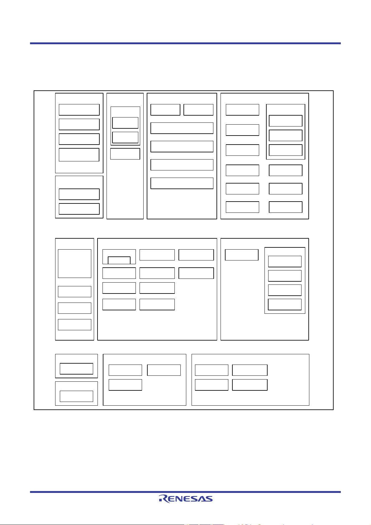
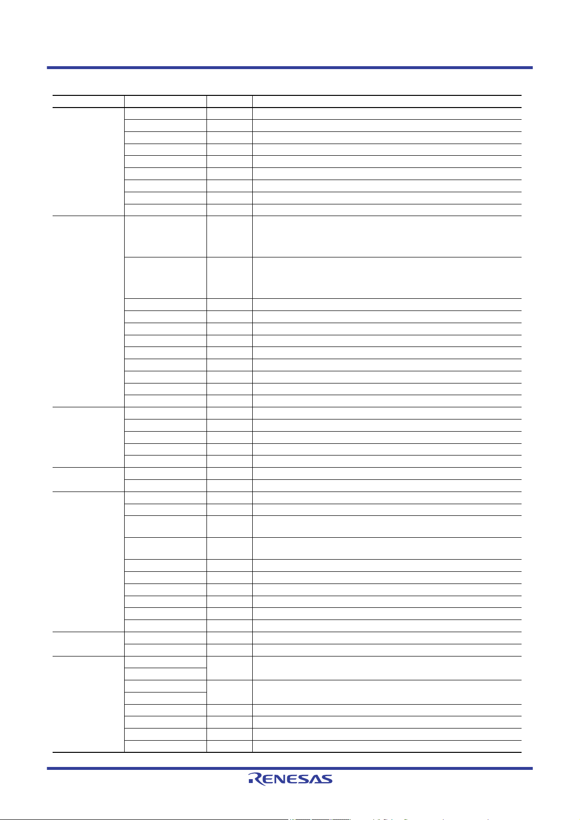
Memory
2 MB code flash
64 KB data flash
640 KB SRAM
DMA
DMAC × 8
System
Mode cont rol
Power cont rol
Register writ e
protection
MOSC/SOSC
Clocks
(H/M/L) OCO
PLL/USBP LL
Battery backup
GPT32 EH x 4
GPT32 E x 4
GPT32 x 6
Timers
AGT × 2
RTC
CTSU
Arm Cortex-M4
DSP FPU
MPU
NVIC
System timer
Test and DBG interf ace
DTC
WDT/IWDT
CAC
POR/LVD
Reset
Human machine interfaces
GLCDC
Graphics
DRW
JPEG codec
PDC
ELC
Event link
SCE7
Security
Analog
CRC
Data processing
DOC
SRC
Communication interfaces
QSPI USBHS
IIC × 3 SDHI × 2
ETHERC
with IEEE 158 8
SPI × 2 CAN × 2
SSIE × 2 USBFS
SCI × 10
IrDA × 1
TSN
DAC12 ACMPHS × 6
ADC12 with
PGA × 2
8 KB St andb y
SRAM
Bus
MPU
CSC
External
SDRAM
KINT
ICU
1.2 Block Diagram
Figure 1.1 shows a block diagram of the MCU superset, some individual devices within the group have a subset of the
features.
Figure 1.1 Block diagram
R01DS0303EU0130 Rev.1.30 Page 10 of 116
Aug 30, 2019
Page 11
S5D9 Datasheet 1. Overview
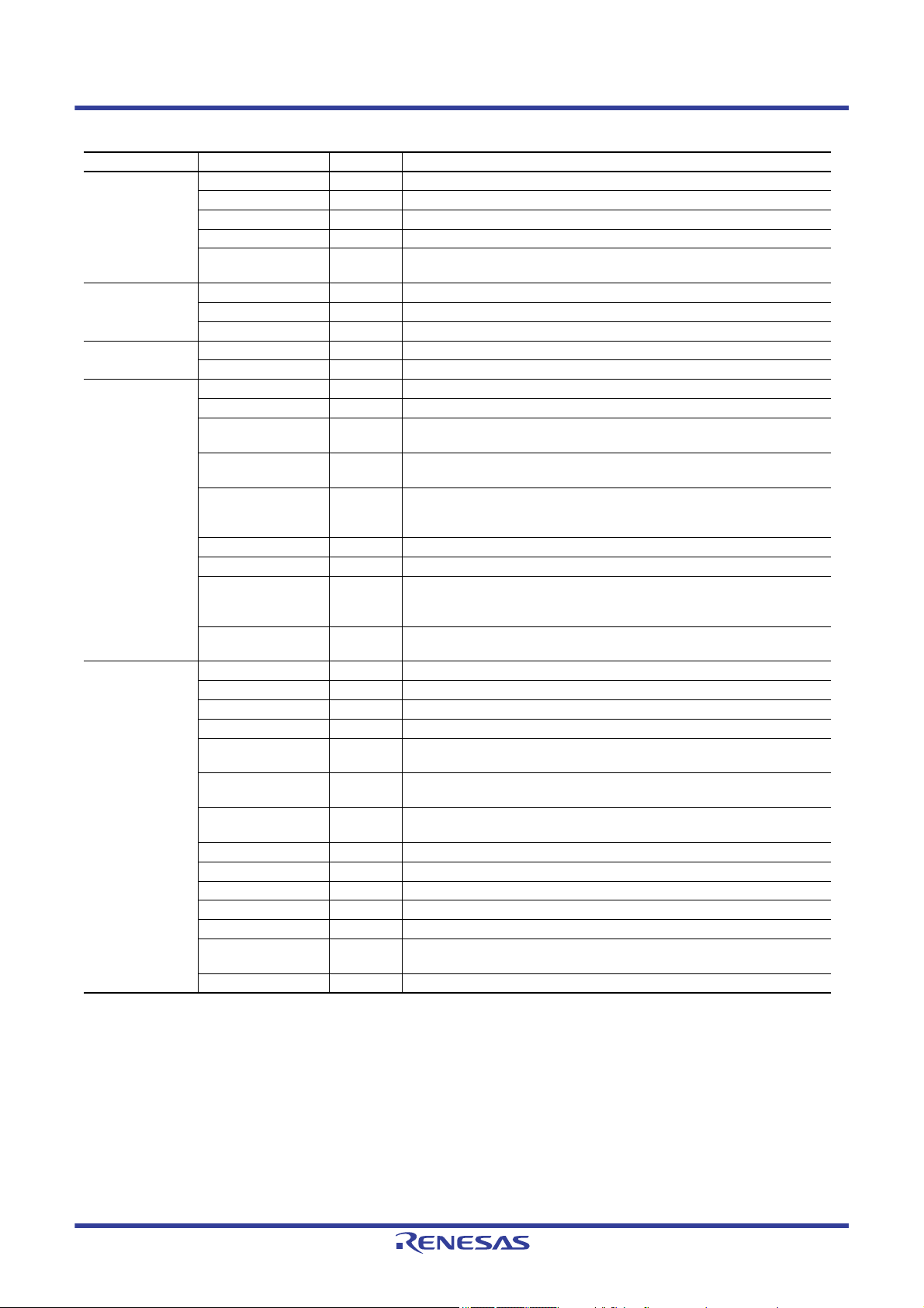
R 7 F S 5 D 9 7
Package type
BG: BGA 176 pins
FC: LQFP 176 pins
FB: LQFP 144 pins
FP: LQFP 100 pins
LK: LGA 145 pins
Quality ID
Software ID
Operating temperature
2: -40
°
C to 85°C
3: -40
°
C to 105°C
Code flash memory size
C: 1 MB
E: 2 MB
Feature set
7: Superset
Group name
D9: S5D9 Group, Arm Cortex-M4, 120 MHz
Series name
5: High integration
Renesas Synergy family
Flash memory
Renesas microcontroller
Renesas
E 2 A 0 1 C B G
# A C
0
Packaging, Terminal material (Pb-free)
#AA: T ray/Sn ( Tin) only
#AC: Tray/others
Production identification code
1.3 Part Numbering
Figure 1.2 Part numbering scheme
Table 1.14 Product list
Product part number Orderable part number Package code
R7FS5D97E2A01CBG R7FS5D97E2A01CBG#AC0 PLBG0176GE-A 2 MB 64 KB 640 KB -40 to +85°C
R7FS5D97E3A01CFC R7FS5D97E3A01CFC#AA0 PLQP0176KB-A -40 to +105°C
R7FS5D97E2A01CLK R7FS5D97E2A01CLK#AC0 PTLG0145KA-A -40 to +85°C
R7FS5D97E3A01CFB R7FS5D97E3A01CFB#AA0 PLQP0144KA-B -40 to +105°C
R7FS5D97E3A01CFP R7FS5D97E3A01CFP#AA0 PLQP0100KB-B -40 to +105°C
R7FS5D97C2A01CBG R7FS5D97C2A01CBG#AC0 PLBG0176GE-A 1 MB -40 to +85°C
R7FS5D97C3A01CFC R7FS5D97C3A01CFC#AA0 PLQP0176KB-A -40 to +105°C
R7FS5D97C2A01CLK R7FS5D97C2A01CLK#AC0 PTLG0145KA-A -40 to +85°C
R7FS5D97C3A01CFB R7FS5D97C3A01CFB#AA0 PLQP0144KA-B -40 to +105°C
R7FS5D97C3A01CFP R7FS5D97C3A01CFP#AA0 PLQP0100KB-B -40 to +105°C
Code
flash
Data
flash SRAM
Operating
temperature
R01DS0303EU0130 Rev.1.30 Page 11 of 116
Aug 30, 2019
Page 12
S5D9 Datasheet 1. Overview
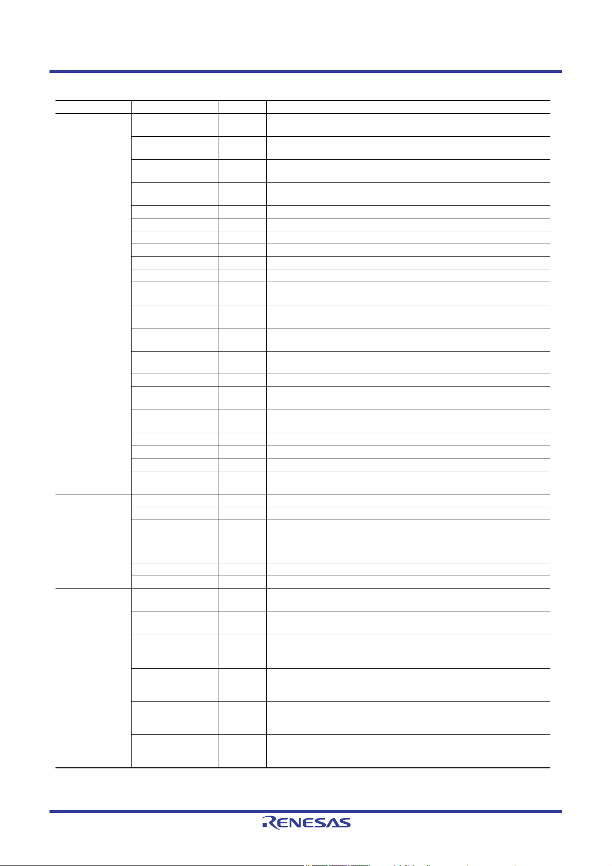
1.4 Function Comparison
Table 1.15 Functional comparison (Graphics)
Part numbers
Function
Pin count 176 176 145 144 100
Package BGA LQFP LGA LQFP LQFP
Code flash memory 2/1 MB
Data flash memory 64 KB
SRAM 640 KB
Parity 608 KB
ECC 32 KB
Standby SRAM 8 KB
System CPU clock 120 MHz
Backup
registers
ICU Yes
KINT 8
Event link ELC Yes
DMA DTC Yes
DMAC 8
BUS External bus 16-bit bus 8-bit bus
SDRAM Yes No
Timers GPT32EH 4 4 4 4 4
GPT32E44444
GPT32 6 6 6 6 5
AGT 2 2 2 2 2
RTC Yes
WDT/IWDT Yes
Communication SCI 10
IIC 3 2
SPI 2
SSIE 2 1
QSPI 1
SDHI 2
CAN 2
USBFS Yes
USBHS Yes No
ETHERC 1
Analog ADC12 24 22 19
DAC12 2
ACMPHS 6
TSN Yes
HMI CTSU 13 18 12
Graphics GLCDC RGB888
DRW Yes
JPEG Yes
PDC Yes
Data processing CRC Yes
DOC Yes
SRC Yes
Security SCE7
R7FS5D97E2XXXCBG/
R7FS5D97C2XXXCBG
R7FS5D97E3XXXCFC/
R7FS5D97C3XXXCFC
R7FS5D97E2XXXCLK/
R7FS5D97C2XXXCLK
512 B
R7FS5D97E3XXXCFB/
R7FS5D97C3XXXCFB
R7FS5D97E3XXXCFP/
R7FS5D97C3XXXCFP
R01DS0303EU0130 Rev.1.30 Page 12 of 116
Aug 30, 2019
Page 13
S5D9 Datasheet 1. Overview
1.5 Pin Functions
Table 1.16 Pin functions (1 of 5)
Function Signal I/O Description
Power supply VCC Input Digital voltage supply pin. This is used as the digital power supply for the
respective modules and internal voltage regulator, and used to monitor the
voltage of the POR/LVD. Connect to the system power supply. Connect to
VSS through a 0.1-μF smoothing capacitor close to each VCC pin.
VCL0 - Connect to VSS through a 0.1-μF smoothing capacitor close to each VCL
VCL -
VSS Input Ground pin. Connect to the system power supply (0 V).
VBATT Input Backup power pin
Clock XTAL Output Pins for a crystal resonator. An external clock signal can be input through the
EXTAL Input
XCIN Input Input/output pins for the sub-clock oscillator. Connect a crystal resonator
XCOUT Output
EBCLK Output Outputs the external bus clock for external devices
SDCLK Output Outputs the SDRAM-dedicated clock
CLKOUT Output Clock output pin
Operating mode
control
System control RES Input Reset signal input pin. The MCU enters the reset state when this signal goes
CAC CACREF Input Measurement reference clock input pin
Interrupt NMI Input Non-maskable interrupt request pin
KINT KR00 to KR07 Input A key interrupt can be generated by inputting a falling edge to the key
On-chip emulator TMS I/O On-chip emulator or boundary scan pins
External bus
interface
MD Input Pin for setting the operating mode. The signal level on this pin must not be
IRQ0 to IRQ15 Input Maskable interrupt request pins
TDI Input
TCK Input
TDO Output
TCLK Output This pin outputs the clock for synchronization with the trace data
TDATA0 to TDATA3 Output Trace data output
SWDIO I/O Serial wire debug data input/output pin
SWCLK Input Serial wire clock pin
SWO Output Serial wire trace output pin
RD Output Strobe signal indicating that reading from the external bus interface space is
WR Output Strobe signal indicating that writing to the external bus interface space is in
WR0 to WR1 Output Strobe signals indicating that either group of data bus pins (D07 to D00 or
BC0 to BC1 Output Strobe signals indicating that either group of data bus pins (D07 to D00 or
ALE Output Address latch signal when address/data multiplexed bus is selected
WAIT Input Input pin for wait request signals in access to the external space, active low
CS0 to CS7 Output Select signals for CS areas, active low
A00 to A23 Output Address bus
D00 to D15 I/O Data bus
A00/D00 to A15/D15 I/O Address/data multiplexed bus
pin. Stabilize the internal power supply.
EXTAL pin.
between XCOUT and XCIN.
changed during operation mode transition on release from the reset state.
low.
interrupt input pins
in progress, active low
progress, in 1-write strobe mode, active low
D15 to D08) is valid in writing to the external bus interface space, in byte
strobe mode, active low
D15 to D08) is valid in access to the external bus interface space, in 1-write
strobe mode, active low
R01DS0303EU0130 Rev.1.30 Page 13 of 116
Aug 30, 2019
Page 14
S5D9 Datasheet 1. Overview
Table 1.16 Pin functions (2 of 5)
Function Signal I/O Description
SDRAM interface CKE Output SDRAM clock enable signal
SDCS Output SDRAM chip select signal, active low
RAS Output SDRAM low address strobe signal, active low
CAS Output SDRAM column address strobe signal, active low
WE Output SDRAM write enable signal, active low
DQM0 Output SDRAM I/O data mask enable signal for DQ07 to DQ00
DQM1 Output SDRAM I/O data mask enable signal for DQ15 to DQ08
A00 to A15 Output Address bus
DQ00 to DQ15 I/O Data bus
GPT GTETRGA,
GTETRGB,
GTETRGC,
GTETRGD
GTIOC0A to
GTIOC13A,
GTIOC0B to
GTIOC13B
GTIU Input Hall sensor input pin U
GTIV Input Hall sensor input pin V
GTIW Input Hall sensor input pin W
GTOUUP Output 3-phase PWM output for BLDC motor control (positive U phase)
GTOULO Output 3-phase PWM output for BLDC motor control (negative U phase)
GTOVUP Output 3-phase PWM output for BLDC motor control (positive V phase)
GTOVLO Output 3-phase PWM output for BLDC motor control (negative V phase)
GTOWUP Output 3-phase PWM output for BLDC motor control (positive W phase)
GTOWLO Output 3-phase PWM output for BLDC motor control (negative W phase)
AGT AGTEE0, AGTEE1 Input External event input enable signals
AGTIO0, AGTIO1 I/O External event input and pulse output pins
AGTO0, AGTO1 Output Pulse output pins
AGTOA0, AGTOA1 Output Output compare match A output pins
AGTOB0, AGTOB1 Output Output compare match B output pins
RTC RTCOUT Output Output pin for 1-Hz or 64-Hz clock
RTCIC0 to RTCIC2 Input Time capture event input pins
SCI SCK0 to SCK9 I/O Input/output pins for the clock (clock synchronous mode)
RXD0 to RXD9 Input Input pins for received data (asynchronous mode/clock synchronous mode)
TXD0 to TXD9 Output Output pins for transmitted data (asynchronous mode/clock synchronous
CTS0_RTS0 to
CTS9_RTS9
SCL0 to SCL9 I/O Input/output pins for the I
SDA0 to SDA9 I/O Input/output pins for the I
SCK0 to SCK9 I/O Input/output pins for the clock (simple SPI mode)
MISO0 to MISO9 I/O Input/output pins for slave transmission of data (simple SPI mode)
MOSI0 to MOSI9 I/O Input/output pins for master transmission of data (simple SPI mode)
SS0 to SS9 Input Chip-select input pins (simple SPI mode), active low
IIC SCL0 to SCL2 I/O Input/output pins for the clock
SDA0 to SDA2 I/O Input/output pins for data
SSIE SSIBCK0 I/O SSIE serial bit clock pins
SSIBCK1
SSILRCK0/SSIFS0 I/O LR clock/frame synchronization pins
SSILRCK1/SSIFS1
SSITXD0 Output Serial data output pins
SSIRXD0 Input Serial data input pins
SSIDATA1 I/O Serial data input/output pins
AUDIO_CLK Input External clock pin for audio (input oversampling clock)
Input External trigger input pins
I/O Input capture, output compare, or PWM output pins
mode)
I/O Input/output pins for controlling the start of transmission and reception
(asynchronous mode/clock synchronous mode), active low
2
C clock (simple IIC mode)
2
C data (simple IIC mode)
R01DS0303EU0130 Rev.1.30 Page 14 of 116
Aug 30, 2019
Page 15
S5D9 Datasheet 1. Overview
Table 1.16 Pin functions (3 of 5)
Function Signal I/O Description
SPI RSPCKA, RSPCKB I/O Clock input/output pin
MOSIA, MOSIB I/O Input or output pins for data output from the master
MISOA, MISOB I/O Input or output pins for data output from the slave
SSLA0, SSLB0 I/O Input or output pin for slave selection
SSLA1 to SSLA3,
SSLB1 to SSLB3
QSPI QSPCLK Output QSPI clock output pin
QSSL Output QSPI slave output pin
QIO0 to QIO3 I/O Data0 to Data3
CAN CRX0, CRX1 Input Receive data
CTX0, CTX1 Output Transmit data
USBFS VCC_USB Input Power supply pins
VSS_USB Input Ground pins
USB_DP I/O D+ I/O pin of the USB on-chip transceiver. Connect this pin to the D+ pin of
USB_DM I/O D- I/O pin of the USB on-chip transceiver. Connect this pin to the D- pin of
USB_VBUS Input USB cable connection monitor pin. Connect this pin to VBUS of the USB
USB_EXICEN Output Low-power control signal for external power supply (OTG) chip
USB_VBUSEN Output VBUS (5 V) supply enable signal for external power supply chip
USB_OVRCURA,
USB_OVRCURB
USB_ID Input Connect the MicroAB connector ID input signal to this pin during operation in
USBHS VCC_USBHS Input Power supply pin
VSS1_USBHS Input Ground pin
VSS2_USBHS Input Ground pin
AVCC_USBHS Input Analog power supply pin for the USBHS
AVSS_USBHS Input Analog ground pin for the USBHS. Must be shorted to the PVSS_USBHS
PVSS_USBHS Input PLL circuit ground pin for the USBHS. Must be shorted to the AVSS_USBHS
USBHS_RREF I/O USBHS reference current source pin. Connect this pin to the AVSS_USBHS
USBHS_DP I/O USB bus D+ data pin
USBHS_DM I/O USB bus D- data pin
USBHS_EXICEN Output Connect this pin to the OTG power supply IC
USBHS_ID Input Connect this pin to the OTG power supply IC
USBHS_VBUSEN Output VBUS power enable signal for USB
USBHS_OVRCURA,
USBHS_OVRCURB
USBHS_VBUS Input USB cable connection monitor input pin
Output Output pins for slave selection
the USB bus
the USB bus
bus. The VBUS pin status (connected or disconnected) can be detected
when the USB module is operating as a function controller.
Input Connect the external overcurrent detection signals to these pins. Connect
the VBUS comparator signals to these pins when the OTG power supply
chip is connected.
OTG mode
pin
pin
pin through a 2.2-kΩ resistor (1%)
Input Overcurrent pin for USB
R01DS0303EU0130 Rev.1.30 Page 15 of 116
Aug 30, 2019
Page 16
S5D9 Datasheet 1. Overview
Table 1.16 Pin functions (4 of 5)
Function Signal I/O Description
ETHERC REF50CK0 Input 50-MHz reference clock. This pin inputs reference signal for
transmission/reception timing in RMII mode.
RMII0_CRS_DV Input Indicates carrier detection signals and valid receive data on RMII0_RXD1
RMII0_TXD0,
RMII0_TXD1
RMII0_RXD0,
RMII0_RXD1
RMII0_TXD_EN Output Output pin for data transmit enable signal in RMII mode
RMII0_RX_ER Input Indicates an error occurred during reception of data in RMII mode
ET0_CRS Input Carrier detection/data reception enable signal
ET0_RX_DV Input Indicates valid receive data on ET0_ERXD3 to ET0_ERXD0
ET0_EXOUT Output General-purpose external output pin
ET0_LINKSTA Input Input link status from the PHY-LSI
ET0_ETXD0 to
ET0_ETXD3
ET0_ERXD0 to
ET0_ERXD3
ET0_TX_EN Output Transmit enable signal. Functions as signal indicating that transmit data is
ET0_TX_ER Output Transmit error pin. Functions as signal notifying the PHY_LSI of an error
ET0_RX_ER Input Receive error pin. Functions as signal to recognize an error during reception
ET0_TX_CLK Input Transmit clock pin. This pin inputs reference signal for output timing from
ET0_RX_CLK Input Receive clock pin. This pin inputs reference signal for input timing to
ET0_COL Input Input collision detection signal
ET0_WOL Output Receive Magic packets
ET0_MDC Output Output reference clock signal for information transfer through ET0_MDIO.
ET0_MDIO I/O Input or output bidirectional signal for exchange of management data with
SDHI SD0CLK, SD1CLK Output SD clock output pins
SD0CMD, SD1CMD I/O Command output pin and response input signal pins
SD0DAT0 to
SD0DAT7,
SD1DAT0 to
SD1DAT7
SD0CD, SD1CD Input SD card detection pins
SD0WP, SD1WP Input SD write-protect signals
Analog power
supply
AVCC0 Input Analog voltage supply pin. This is used as the analog power supply for the
AVSS0 Input Analog ground pin. This is used as the analog ground for the respective
VREFH0 Input Analog reference voltage supply pin for the ADC12 (unit 0). Connect this pin
VREFL0 Input Analog reference ground pin for the ADC12. Connect this pin to VSS when
VREFH Input Analog reference voltage supply pin for the ADC12 (unit 1) and D/A
VREFL Input Analog reference ground pin for the ADC12 and D/A Converter. Connect this
Output 2-bit transmit data in RMII mode
Input 2-bit receive data in RMII mode
Output 4 bits of MII transmit data
Input 4 bits of MII receive data
I/O SD and MMC data bus pins
and RMII0_RXD0 in RMII mode
ready on ET0_ETXD3 to ET0_ETXD0
during transmission
ET0_TX_EN, ET0_ETXD3 to ET0_ETXD0, and ET0_TX_ER
ET0_RX_DV, ET0_ERXD3 to ET0_ERXD0, and ET0_RX_ER
PHY-LSI
respective modules. Supply this pin with the same voltage as the VCC pin.
modules. Supply this pin with the same voltage as the VSS pin.
to VCC when not using the ADC12 (unit 0) and sample-and-hold circuit for
AN000 to AN002.
not using the ADC12 (unit 0) and sample-and-hold circuit for AN000 to
AN002
Converter. Connect this pin to VCC when not using the ADC12 (unit 1),
sample-and-hold circuit for AN100 to AN102, and D/A Converter.
pin to VSS when not using the ADC12 (unit 1), sample-and-hold circuit for
AN100 to AN102, and D/A Converter.
R01DS0303EU0130 Rev.1.30 Page 16 of 116
Aug 30, 2019
Page 17
S5D9 Datasheet 1. Overview
Table 1.16 Pin functions (5 of 5)
Function Signal I/O Description
ADC12 AN000 to AN007,
AN016 to AN020
AN100 to AN103,
AN105 to AN107,
AN116 to AN119
ADTRG0 Input Input pins for the external trigger signals that start the A/D conversion
ADTRG1 Input
PGAVSS000/PGAVS
S100
DAC12 DA0, DA1 Output Output pins for the analog signals processed by the D/A converter
ACMPHS VCOUT Output Comparator output pin
IVREF0 to IVREF3 Input Reference voltage input pins for comparator
IVCMP0 to IVCMP2 Input Analog voltage input pins for comparator
CTSU TS00 to TS17 Input Capacitive touch detection pins (touch pins)
TSCAP - Secondary power supply pin for the touch driver
I/O ports P000 to P007 Input General-purpose input pins
P008 to P010,
P014, P015
P100 to P115 I/O General-purpose input/output pins
P200 Input General-purpose input pin
P201 to P214 I/O General-purpose input/output pins
P300 to P315 I/O General-purpose input/output pins
P400 to P415 I/O General-purpose input/output pins
P500 to P508,
P511 to P513
P600 to P615 I/O General-purpose input/output pins
P700 to P713 I/O General-purpose input/output pins
P800 to P806 I/O General-purpose input/output pins
P900, P901,
P905 to P908
PA00, PA01,
PA08 to PA10
PB00, PB01 I/O General-purpose input/output pins
GLCDC LCD_DATA23 to
LCD_DATA00
LCD_TCON3 to
LCD_TCON0
LCD_CLK Output Panel clock output pin
LCD_EXTCLK Input Panel clock source input pin
PDC PIXCLK Input Image transfer clock pin
VSYNC Input Vertical synchronization signal pin
HSYNC Input Horizontal synchronization signal pin
PIXD0 to PIXD7 Input 8-bit image data pins
PCKO Output Output pin for dot clock
Input Input pins for the analog signals to be processed by the ADC12
Input
Input Differential input pins
I/O General-purpose input/output pins
I/O General-purpose input/output pins
I/O General-purpose input/output pins
I/O General-purpose input/output pins
Output Data output pins for panel
Output Output pins for panel timing adjustment
R01DS0303EU0130 Rev.1.30 Page 17 of 116
Aug 30, 2019
Page 18
S5D9 Datasheet 1. Overview
P201/MD
N P RK L MG H JD E FA B C
N P RK L MG H JD E FA B C
P401
P512
P805
P000
P002
P005
VREFH0
VREFH
P014
P508
P506
P502
P500
P803
P801
P405
P402
P511
P806
P004
P008
VREFL0
VREFL
P015
P505
P504
P501
P804
P802
P100
P700
P406
P400
P513
P001
P006
AVSS0
AVCC0
VSS
P507
P503
VCC
P800
P101
P103
P703
P701
P404
P403
VCC
VSS
P009
P010
VCC
P007
P003
VSS
P102
P104
P106
P707
P706
P704
P702
VSS
P105
P107
P600
VCL0
VBATT
PB01
P705
VCC
P603
P601
P602
XCIN
XCOUT
VSS
PB00
P607
P604
P605
P606
P212
/EXTAL
P213
/XTAL
AVCC_
USB HS
VCC
PA00
VSS
PA01
VCL
PVSS_
USB HS
AVSS_
USB HS
USBHS_
RREF
VSS2_
USB HS
PA09
VCC
PA10
PA08
USBHS_
DM
USBHS_
DP
VCC_
USBHS
VSS1_
USBHS
P613
P610
P614
P615
P708
P415
P413
P205
VSS
VCC
P611
P612
P414
P412
P408
P206
P203
VSS
VCC
P908
P907
P311
VCC
P111
P110/TDI
P608
P609
P411
P410
VSS_
USB
P207
P314
P901
RES
P200
P312
P307
VSS
P300/TCK
/SWCLK
P108/TM S
SWDIO
P114
P115
P409
USB_DM
VCC_
USB
P202
P315
P211
P209
P905
P309
P305
P304
P302
P112
P113
P407
USB_DP
P204
P313
P900
P214
P210
P208
P906
P310
P308
P306
P303
P301
P109/TDO
15
14
13
12
11
10
9
8
7
6
5
4
3
2
1
15
14
13
12
11
10
9
8
7
6
5
4
3
2
1
R7FS5D9XX2XXXCBG
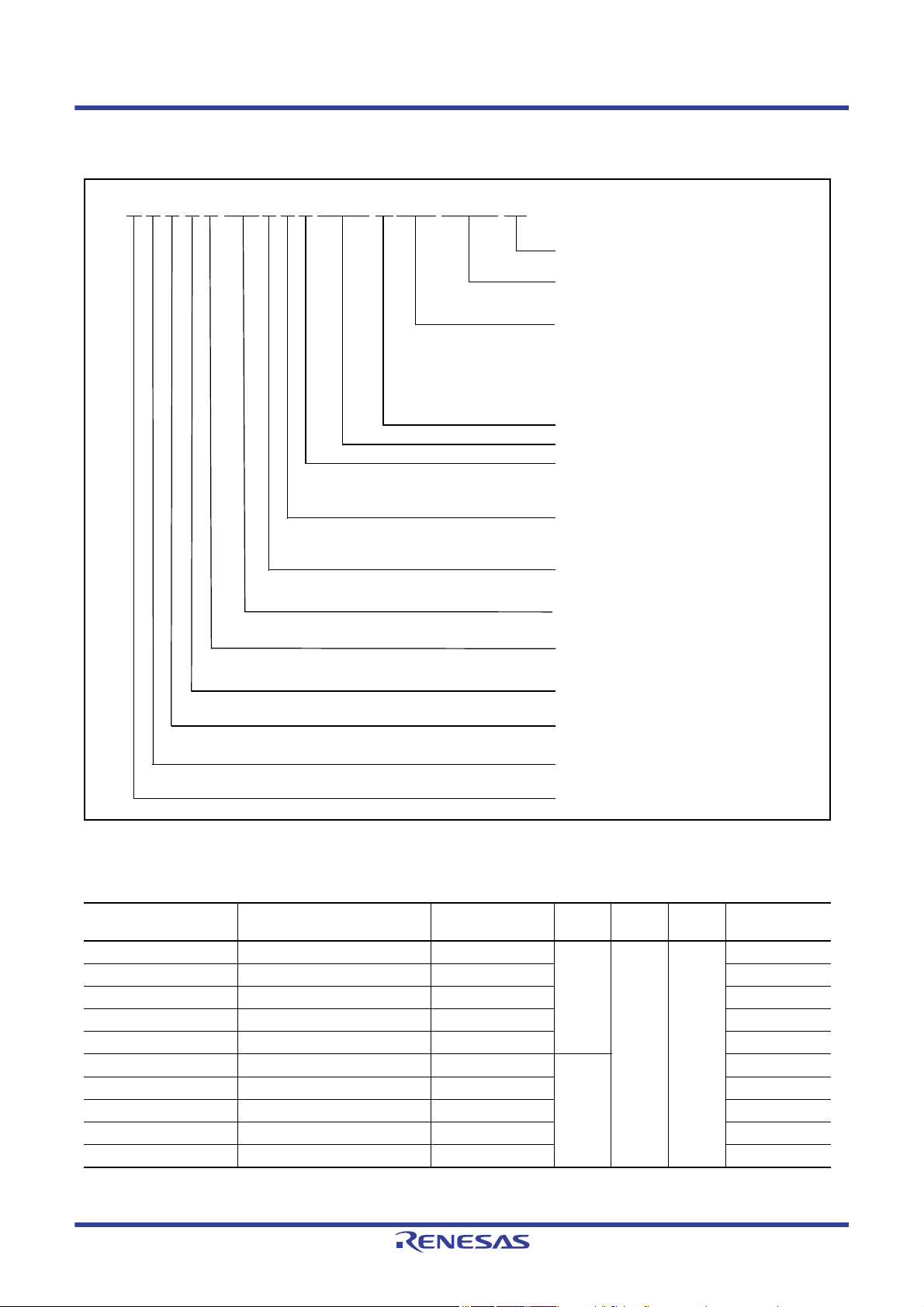
1.6 Pin Assignments
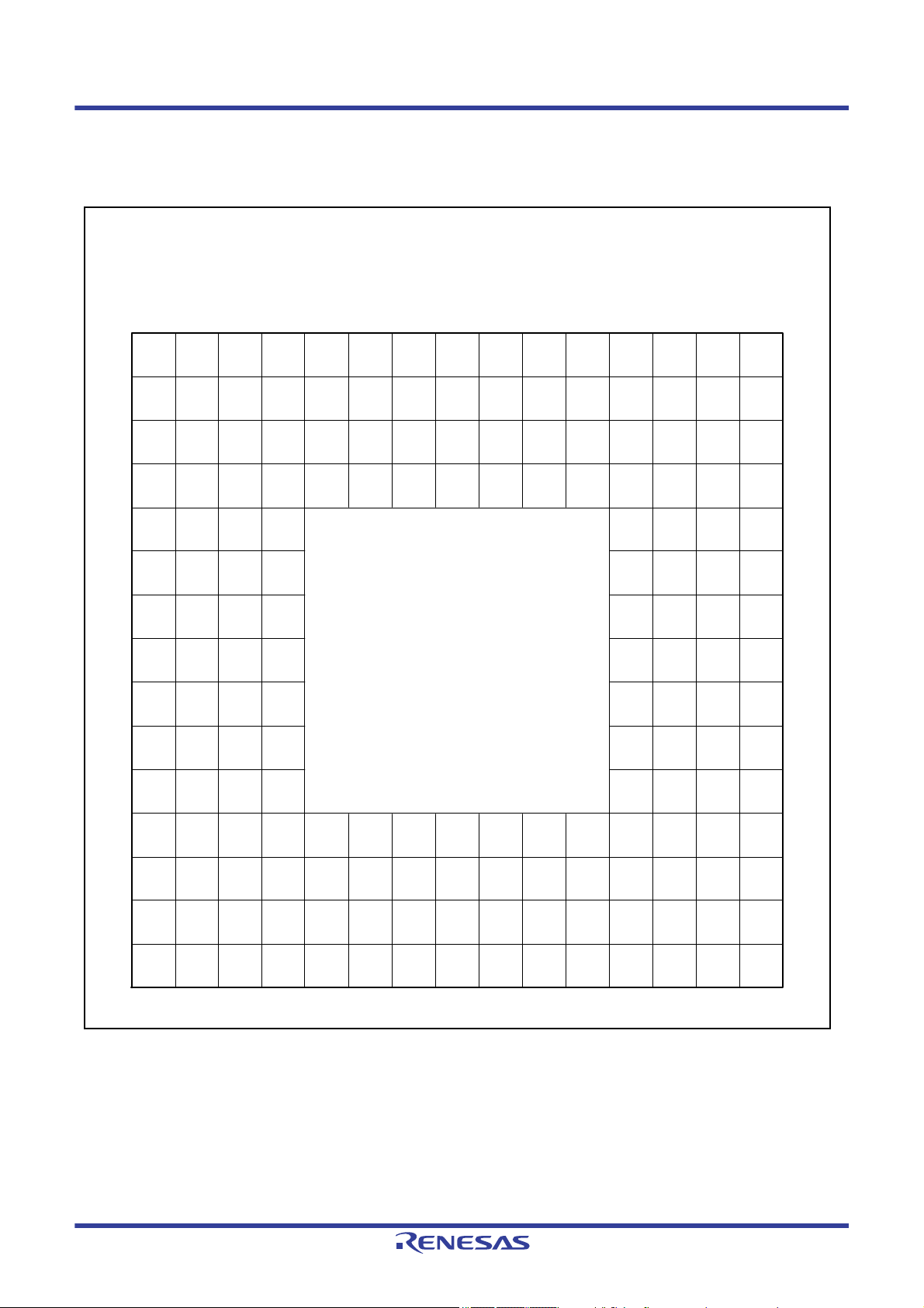
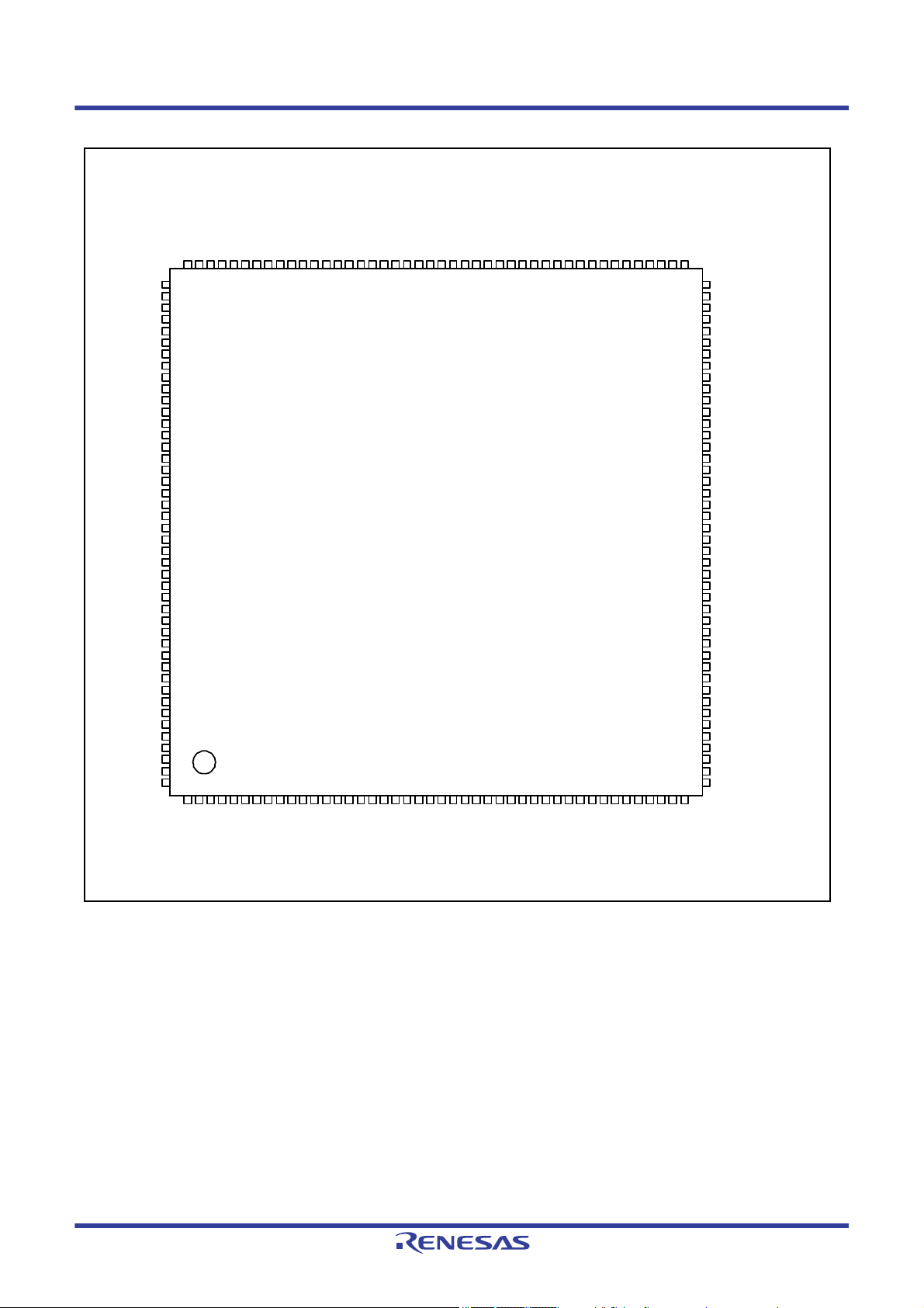
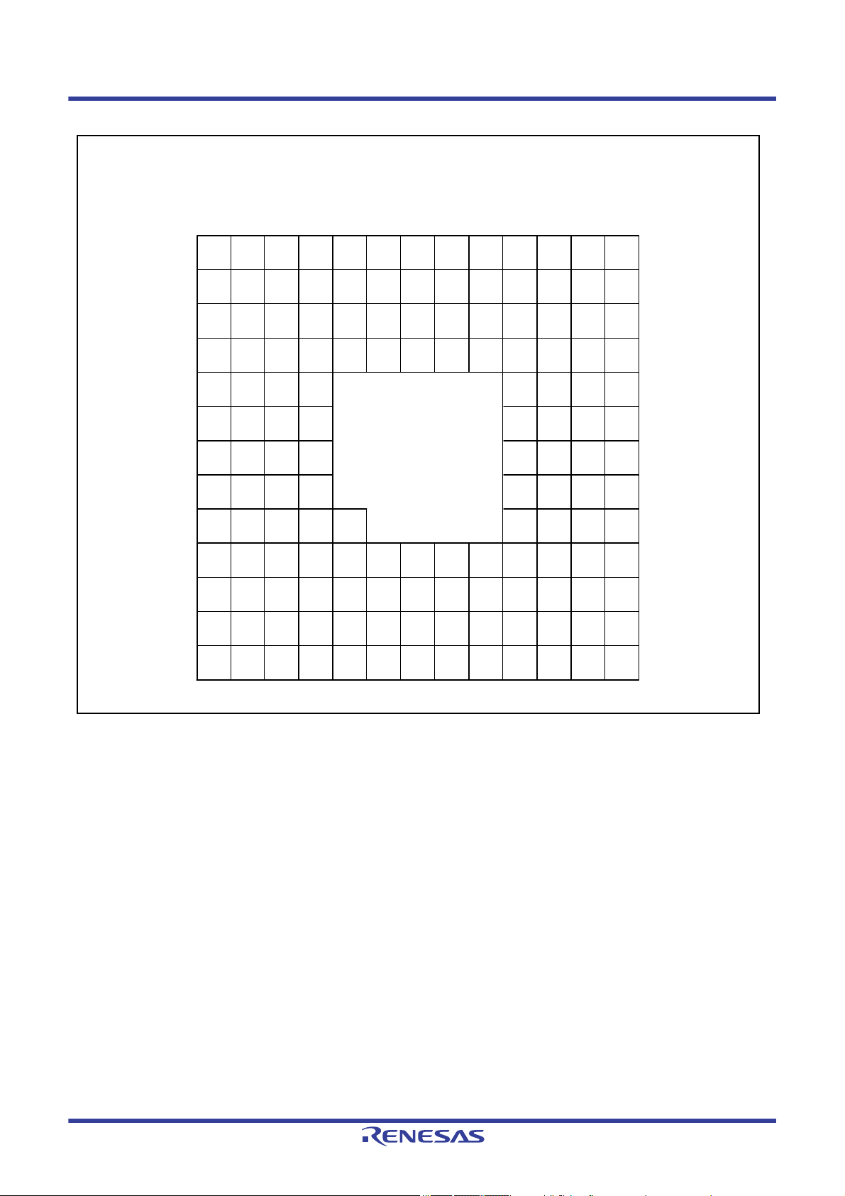
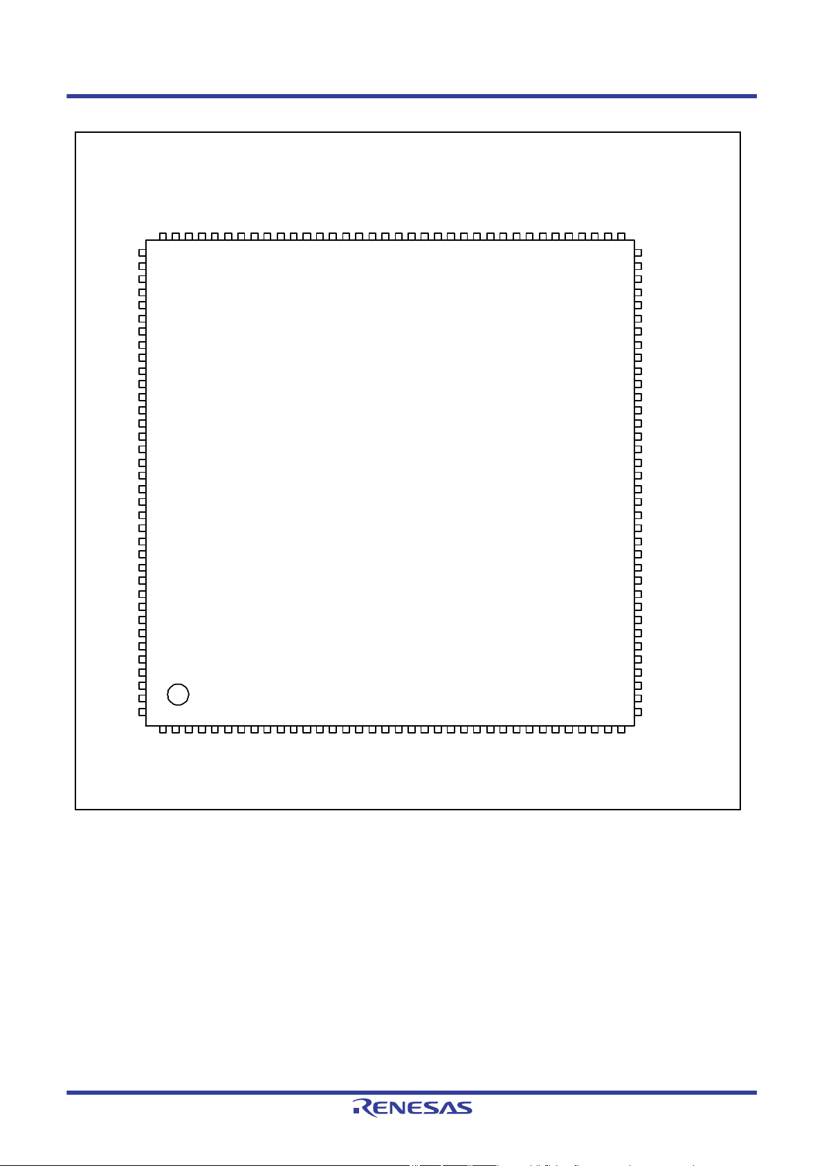
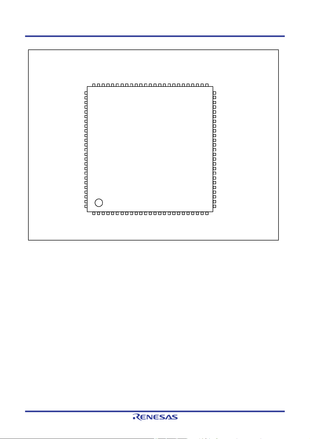
Figure 1.3 to Figure 1.7 show the pin assignments.
Figure 1.3 Pin assignment for 176-pin BGA (top view)
R01DS0303EU0130 Rev.1.30 Page 18 of 116
Aug 30, 2019
Page 19
S5D9 Datasheet 1. Overview
12345678910111213141516171819202122232425262728293031323334353637383940414243
44
132
131
130
129
128
127
126
125
124
123
122
121
120
119
118
117
116
115
114
113
112
111
110
109
108
107
106
105
104
103
102
101
100
9998979695949392919089
88
87
86
85
84
83
82
81
80
79
78
77
76
75
74
73
72
71
70
69
68
67
66
65
64
63
62
61
60
59
58
57
56
55
54
53
52
51
50
49
48
47
46
45
133
134
135
136
137
138
139
140
141
142
143
144
145
146
147
148
149
150
151
152
153
154
155
156
157
158
159
160
161
162
163
164
165
166
167
168
169
170
171
172
173
174
175
176
P802
P803
P804
VCC
VSS
P500
P501
P502
P503
P504
P505
P506
P508
VCC
VSS
P015
P014
VREFL
VREFH
AVCC0
AVSS0
VREFL0
VREFH0
P010
P008
P006
P004
P002
P000
VCC
P805
P511
P801
P507
P512
VSS_USB
P100
P102
P103
P104
P105
P106
P107
VSS
VCC
P600
P601
P602
P603
P605
P606
P607
PA00
PA01
VCL
VSS
VCC
PA10
PA09
PA08
P615
P613
P612
P609
P608
VCC
P114
P112
P108/TMS/SWDIO
P101
P604
P109/TDO
P400
P402
P403
P404
P405
P406
P700
P701
P702
P703
P704
P705
P706
PB00
PB01
VBATT
VCL0
XCIN
XCOUT
VSS
P213/XTAL
VCC
USBHS_RREF
US BHS_D M
VSS1_USBHS
P708
P414
P412
P410
P409
P407
P212/EXTAL
P401
P707
PVSS_USBH S
P800
AVCC_USBHS
AVSS_USBH S
VSS2_USBHS
USBHS_DP
VCC_USBHS
P415
P413
P411
P408
USB_DM
USB_DP
VCC_USB
P207
P206
P205
P204
P203
P202
P313
P314
P315
P900
P901
VSS
VCC
P214
P210
P209
P312
P310
P309
P308
P307
P306
P305
P304
VSS
VCC
P211
P208
RES
P201/MD
P200
P908
P907
P906
P905
P311
P303
P302
P301
P300/TCK/SWCLK
P614
P611
P610
VSS
P115
P113
P110/TDI
P111
P009
P007
P005
P003
P001
VSS
P513
P806
R7FS5D9XX3XXXCFC
Figure 1.4 Pin assignment for 176-pin LQFP (top view)
R01DS0303EU0130 Rev.1.30 Page 19 of 116
Aug 30, 2019
Page 20
S5D9 Datasheet 1. Overview
P400
VCC
VSS
P001
P008
VREFH0
VREFH
P014
VCC
P508
VCC
P801
P100
P402
P511
P512
P002
P009
VREFL0
VREFL
P015
VSS
P501
VSS
P101
P102
P405
P404
P401
P000
P006
AVSS0
AVCC0
P506
P504
P502
P104
P800
P103
P702
P701
P403
P003
P004
P005
P007
P505
P503
P500
P106
VCC
VSS
VCL0
VBATT
P703
P406
P105
P107
P601
P602
XCIN
XCOUT
P704
P700
P600
P603
P605
VCL
P212
/EXTAL
P213
/XTAL
P705
P713
P604
P614
VSS
VCC
VCC
VSS
P712
P709
P608
P610
P612
P613
P711
P710
P415
P413
P114
P115
P609
P611
P708
P414
P411
P408
VSS
VCC
P310
P305
P303
P109/TDO
P112
VCC
VSS
P412
P410
P207
P204
P202
P200
RES
P312
P308
P304
P301
P111
P113
P409
USB_DP
VSS_
USB
P206
P313
P211
P209
P201/ MD
P311
P306
VCC
P300/TCK
/SWCLK
P110/TDI
P407
USB_D M
VCC_
USB
P205
P203
P214
P210
P208
P309
P307
VSS
P302
P108/TM S
/SWDIO
R7FS5D9XX2XXXCLK
13
12
11
10
9
8
7
6
5
4
3
2
1
13
12
11
10
9
8
7
6
5
4
3
2
1
N K L MG H JD E FA B C
N K L MG H JD E FA B C
NC
Figure 1.5 Pin assignment for 145-pin LGA (top view)
R01DS0303EU0130 Rev.1.30 Page 20 of 116
Aug 30, 2019
Page 21
S5D9 Datasheet 1. Overview
1234567891011121314151617181920212223242526272829303132333435
36
108
107
106
105
104
103
102
101
100
999897969594939291908988878685848382818079787776757473
72
71
70
69
68
67
66
65
64
63
62
61
60
59
58
57
56
55
54
53
52
51
50
49
48
47
46
45
44
43
42
41
40
39
38
37
109
110
111
112
113
114
115
116
117
118
119
120
121
122
123
124
125
126
127
128
129
130
131
132
133
134
135
136
137
138
139
140
141
142
143
144
VCC
VSS
P500
P501
P502
P503
P504
P505
P506
P508
VCC
VSS
P014
VREFL
VREFH
AVCC0
AVSS0
VREFL0
VREFH0
P009
P008
P007
P006
P005
P004
P003
P002
P001
P000
VSS
VCC
P511
P801
P015
P512
P300/TCK/SWCLK
P302
P303
VCC
VSS
P304
P305
P306
P307
P308
P309
P310
P311
P200
P201/MD
RES
P208
P209
P210
P211
P214
VCC
VSS
P313
P202
P203
P204
P205
P206
P207
VCC_USB
USB_DP
VSS_USB
P301
P312
USB_DM
P100
P102
P103
P104
P105
P106
P107
VSS
VCC
P600
P601
P602
P603
P605
VCL
VSS
VCC
P614
P613
P612
P611
P610
P609
P608
VSS
VCC
P115
P114
P113
P112
P111
P110/T DI
P108/TMS/SWDIO
P101
P604
P109/T DO
P400
P402
P403
P404
P405
P406
P700
P701
P702
P703
P704
P705
VBATT
XCIN
XCOUT
VSS
P213/XTAL
P212 /EXTAL
VCC
P713
P712
P711
P710
P708
P415
P414
P413
P412
P411
P410
P409
P407
P401
VCL0
P408
P709
P800
R7F5D9XX3XXXCFB
Figure 1.6 Pin assignment for 144-pin LQFP (top view)
R01DS0303EU0130 Rev.1.30 Page 21 of 116
Aug 30, 2019
Page 22
S5D9 Datasheet 1. Overview
12345678910111213141516171819202122232425
75747372717069686766656463626160595857565554535251
50
49
48
47
46
45
44
43
42
41
40
39
38
37
36
35
34
33
32
31
30
29
28
27
26
76
77
78
79
80
81
82
83
84
85
86
87
88
89
90
91
92
93
94
95
96
97
98
99
100
P502
P503
P504
P508
VCC
VSS
P015
P014
VREFL
VREFH
AVCC0
AVSS0
VREFH0
P008
P007
P006
P005
P004
P003
P002
P001
P501
VREFL0
P300/TCK/SWCLK
P302
P303
VCC
VSS
P304
P305
P306
P307
P200
P201/ MD
RES
P208
P210
P211
P214
P205
P206
P207
VCC_USB
USB_DP
USB_DM
VSS_USB
P301
P209
P100
P102
P103
P104
P105
P106
P107
P600
P601
P602
VCL
VSS
VCC
P609
P608
P115
P114
P113
P112
P111
P110/ TDI
P109/ TDO
P108/TMS/SWDIO
P101
P610
P40 0
P40 2
P40 3
P40 4
P40 5
P40 6
VBATT
VCL0
XCIN
XCOUT
VSS
P213/XTAL
VCC
P70 8
P41 5
P41 4
P41 3
P41 2
P41 1
P41 0
P40 9
P40 7
P40 1
P212/ EXTAL
P500
P000
P40 8
R7FS5D9XX3XXXCFP
Figure 1.7 Pin assignment for 100-pin LQFP (top view)
R01DS0303EU0130 Rev.1.30 Page 22 of 116
Aug 30, 2019
Page 23
S5D9 Datasheet 1. Overview
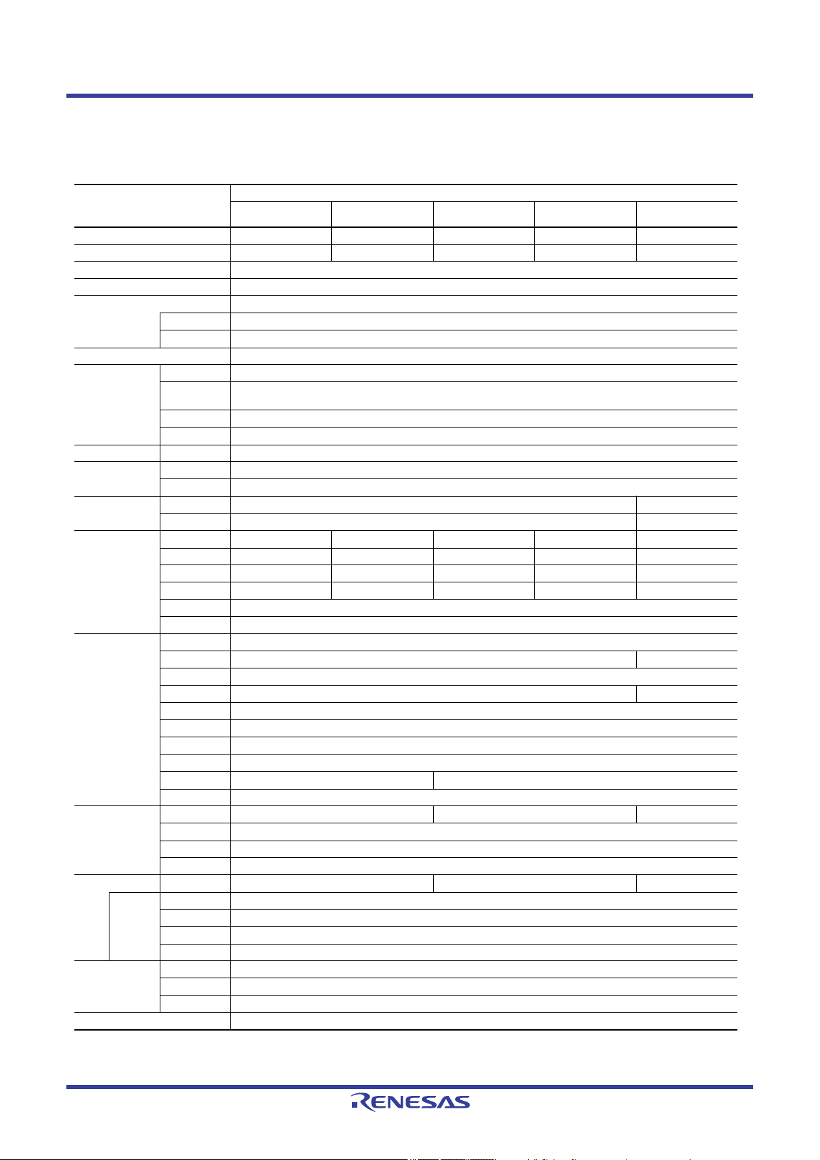
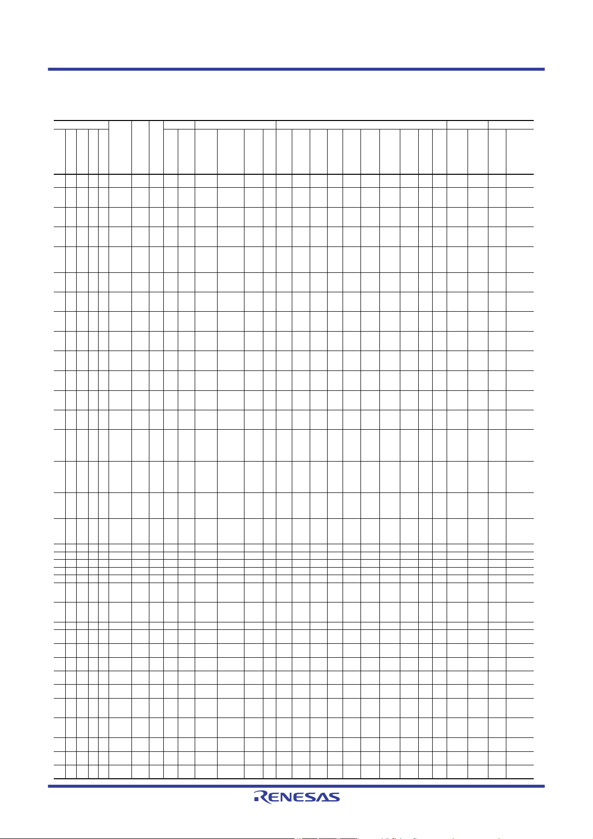
1.7 Pin Lists
Pin number
Power, System,
Clock, Debug,
BGA176
LQFP176
LGA145
N13 1 N13 1 1 - IRQ0 P400 - - AGTIO1 - GTIOC6A- - SCK4 SCK7 SCL0_A-AUDIO
R152L1122- IRQ5-DSP401 - - - GTE TRGA GTIOC6B- CTX0 CTS4_
P14 3 M13 3 3 CACREF IRQ4-DSP402 - - AGTIO0/
M124K1144- - P403- - AGTIO0/
M13 5 L12 5 5 - - P404 - - - - GTIOC3BRTC
P15 6 L13 6 6 - - P40 5 - - - - GTIOC1A-- - - - - SSITX
N147J1077- - P406- - - - GTIOC1B- - - - - SSL B3_CSSIRX
N15 8 H10 8 - - - P700 - - - - GTIOC5A-- - - - MISOB
M14 9 K12 9 - - - P701 - - - - GTIOC5B-- - - - MOSIB_C-ET0_ET
L12 10 K13 10 - - - P702 - - - - GTIOC6A-- - - - RSPC
M1 5 11 J11 11 - - - P 70 3 - - - - GT IOC6B- - - - - SSL B0_C-ET0_ER
L13 12 H11 12 - - - P704 - - AGTO0 - - - CTX0 - - - SSLB1_C-ET0_RX
K12 13 G11 13 - - - P705 - - AGTIO0 - - - CRX0 - - - SSLB2_C-ET0_CRSRMII0_
L14 14 - - - - IRQ7 P706 - - - - - - - - RXD3/
L1515- --- IRQ8P707- - - - - - - - TXD3/
J12 16 - - - - - PB00 - - - - - - - - SCK3 - - - - - USB
K13 17 - - - - - PB01 - - - - - - - - CTS3_
K14 18 J12 14 8 VBATT - - - - - - - - - - - - - - - - - - - - - -
K15 19 J13 15 9 VCL0 - - - - - - - - - - - - - - - - - - - - - -
J15 20 H13 16 10 XCIN - - - - - - - - - - - - - - - - - - - - - -
J14 21 H12 17 11 XCOUT - - - - - - - - - - - - - - - - - - - - - -
J13 22 F12 18 12 VSS - - - - - - - - - - - - - - - - - - - - - -
H14 23 G12 19 13 XTAL IRQ2 P213 - - - GTE TRGC GTIO C0A-- - TXD1/
H15 24 G13 20 14 EXTAL IRQ3 P212 - - AGTEE1 GTETRGD GT IOC0B-- - RXD1/
H12 25 F13 21 15 VCC - - - - - - - - - - - - - - - - - - - - - -
H13 26 - - - AVCC_U
G1327- --USBHS_
G14 28 - - - AVSS_U
G1529- --PVSS_U
G1230- --VSS2_U
F1531- --- - - - - - - - - - - - - - - - - USB
F1432- --- - - - - - - - - - - - - - - - - USB
F1233- --VSS1_U
F13 34 - - - VCC_US
- - G10 22 - - - P713 - - AGTOA0 - GTI OC2A-- - - - - - - - - - - - TS17-
LQFP144
CAC
LQFP100
----- - - ------ - - ---- - --
SBHS
----- - - ------ - - ---- - --
RREF
----- - - ------ - - ---- - --
SBHS
----- - - ------ - - ---- - --
SBHS
----- - - ------ - - ---- - --
SBHS
----- - - ------ - - ---- - --
SBHS
----- - - ------ - - ---- - --
BHS
Extbus Timers Communication interfaces Analog HMI
Interrupt
I/O port
External bus
SDRAM
AGT
GPT
GPT
RTC
USBFS,
CAN
SCI0,2,4,6,8
(30 MHz)
SCI1,3,5,7,9
(30 MHz)
IIC
SPI, QSPI
SSIE
ETHERC (MII)
(25 MHz)
ETHERC (RMII)
(50 MHz)
USBHS
SDHI
--ADTRG1---
--- - - VSYNC
-SD1
---PIXD7
DAT7
_B
-SD1
---PIXD6
DAT6
_B
-SD1
---PIXD5
DAT5
_B
-SD1
---PIXD4
DAT4
_B
-SD1
---PIXD3
DAT3
_B
-SD1
---PIXD2
DAT2
_B
-SD1
---PIXD1
DAT1
_B
-SD1
- VCOUT - PIXD0
DAT0
_B
-SD1
---HSYNC
CLK_
B
-SD1
---PIXCLK
CMD
_B
SD1
---CD_
HS_
B
OVR
CUR
B
SD1
---WP_
HS_
B
OVR
CUR
A
-- - - -
HS_
VBU
SEN
-- - - -
HS_
VBU
S
-- - - -
HS_
DM
-- - - -
HS_
DP
--RTC
AGTIO1
-GTIOC
AGTIO1
3A
TXD7/
RTS4/
SS4
CRX0 - RXD7/
IC0
RTC
-- CTS7_
IC1
-- - -- SSILR
IC2
SDA0_A--ET0_MDCET0_MDC--- - - MOSI7
/SDA7
-- AUDIO
MISO7
/SCL7
-- SSIBC
RTS7/
SS7
_C
KB_C
-- - - - USB
MISO3
/SCL3
-- - - - USB
MOSI3
/SDA3
-- - - - USB
RTS3/
SS3
-- - - - --ADTRG1--MOSI1
/SDA1
-- - - - --- - - MISO1
/SCL1
ET0_WOLET0_
_CLK
_CLK
K0_A
CK0/S
SIFS0_
A
D0_A
D0_A
-ET0_ET
-ET0_ER
ET0_M
DIO
ET0_LI
NKSTA
ET0_EX
OUT
ET0_TX
_EN
ET0_RX
_ER
XD1
XD0
XD1
XD0
_CLK
WOL
ET0_M
DIO
ET0_LI
NKST
A
ET0_E
XOUT
RMII0_
TXD_E
N_B
RMII0_
TXD1_
B
RMII0_
TXD0_
B
REF50
CK0_B
RMII0_
RXD0_
B
RMII0_
RXD1_
B
RMII0_
RX_E
R_B
CRS_
DV_B
ADC12
DAC12,
ACMPHS
CTSU
GLCDC, PDC
R01DS0303EU0130 Rev.1.30 Page 23 of 116
Aug 30, 2019
Page 24
S5D9 Datasheet 1. Overview
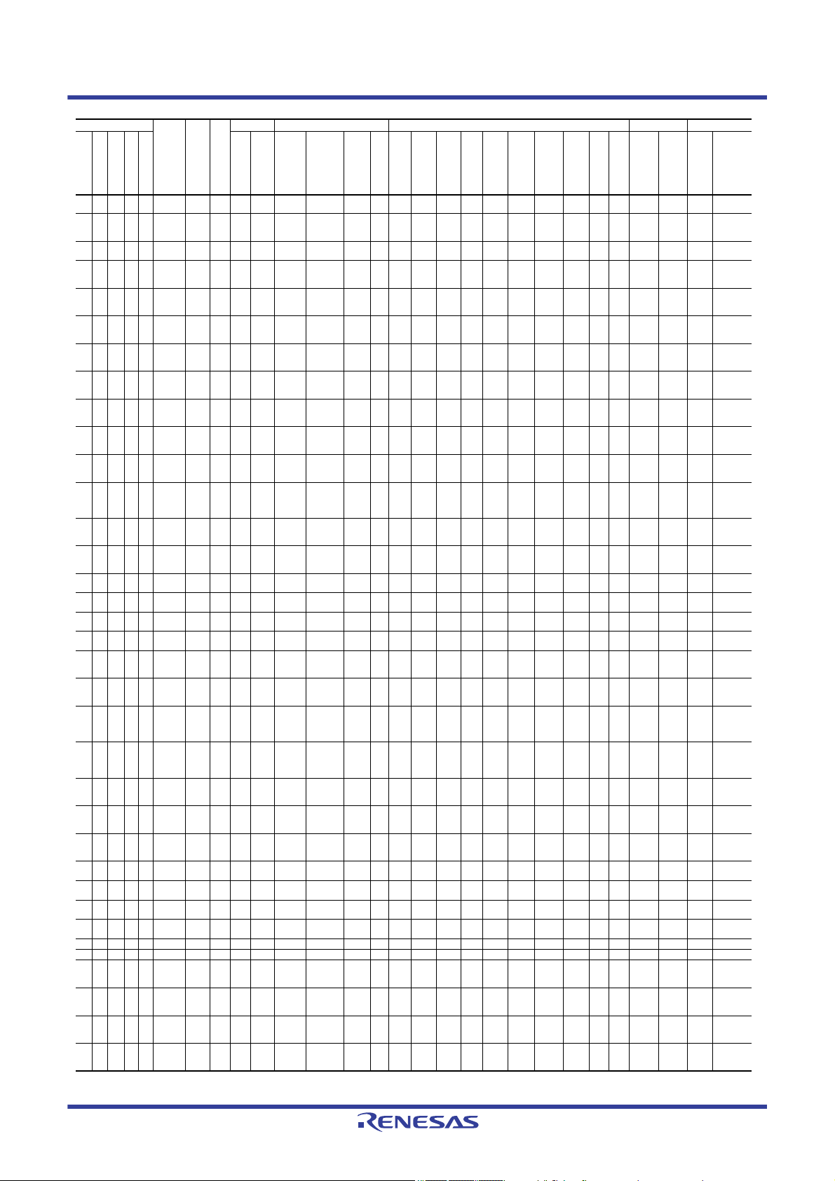
Pin number
Power, System,
Clock, Debug,
BGA176
LQFP176
LGA145
- - F11 23 - - - P71 2 - - AGTOB0 - GTIOC2B-- - - - - - - - - - - - TS16-
- - E13 24 - - - P711 - - AGTEE0 - - - - - CTS1_
- - E12 25 - - - P710 - - - - - - - - SCK1 - - - ET0_TX
- - F10 26 - - IRQ10 P709 - - - - - - - - TXD1/
E15 35 D13 27 16 CACREF IRQ11 P708 - - - - - - - - RXD1/
E14 36 E11 28 17 - IRQ8 P415 - - - - GTIOC0A-USB_
D15 37 D12 29 18 - IRQ9 P414 - - - - GTIOC0B- - - - - SSL A1_B-ET0_RX
E13 38 E10 30 19 - - P413 - - - GTOUUP - - - CTS 0_
D14 39 C13 31 20 - - P412 - - AGTEE1 GTOULO - - - S CK0 - - RSPC
C15 40 D11 32 21 - IRQ4 P411 - - AGTOA1 GTOVUP GTIOC9A-- TXD0/
C14 41 C12 33 22 - IRQ5 P410 - - AGTOB1 GTOVLO GTIOC9B- - RXD0/
B15 42 B13 34 23 - IRQ6 P409 - - - GTOWUP GT IOC
D13 43 D10 35 24 - IRQ7 P408 - - - GTOWLO GTIOC
A15 44 A13 36 25 - - P40 7 - - AGTIO0 - - RTC
C13 45 B11 37 26 VSS_USB----- - - ------ - - ---- - --
B14 46 A12 38 27 - - - - - - - - - USB_DM----- - ---- - --
A14 47 B12 39 28 - - - - - - - - - USB_
B13 48 A11 40 29 VCC_USB----- - - ------ - - ---- - --
C12 49 C11 41 30 - - P207 A17 - - - - - - - - - SSLB2
D12 50 B10 42 31 - IRQ0-DSP206 WAIT - - GTIU - - USB_
E12 51 A10 43 32 CLKOUT IRQ1-DSP205 A16 - AGTO1 G TIV GTIOC4A-USB_
A13 52 C10 44 - CACREF - P204 A18 - AGTIO1 GTIW GTIOC4B-USB_
D11 53 A9 45 - - IRQ2-DSP203 A19 - - - GTIOC5A- CTX0 CTS2_
B12 54 C9 46 - - IRQ3-DSP202 WR1/
A12 55 B9 4 7 - - - P313 A20 - - - - - - - - - - - ET0_ER
C11 56 - - - - - P314 A21 - - - - - - - - - - - - - - - ADTRG0- - LCD_TCO
B11 57 - - - - - P315 A22 - - - - - - RXD4 - - - - - - - - - - - LCD_TCO
A11 58 - - - - - P900 A23 - - - - - - TXD4 - - - - - - - - - - - LCD_CLK_
C10 59 - - - - - P901 - - AGTIO1 - - - - SCK4 - - - - - - - - - - - LCD_DATA
D10 60 D9 48 - VSS - - - - - - - - - - - - - - - - - - - - - -
D9 61 D8 49 - VCC - - - - - - - - - - - - - - - - - - - - - -
A10 62 A8 50 33 TRCLK - P214 - - - GTIU - - - - - - QSPCLK-ET0_MDCET0_MDC-SD0
B10 63 B8 51 34 TRDATA0- P211 - - - GTIV - - - - - - QIO0 - ET0_M
A9 64 A7 52 35 TRDATA1- P210 - - - GTIW - - - - - - QIO1 - ET0_WOLET0_
B9 65 B7 53 36 TRDATA2- P209 - - - GTOVUP - - - - - - QIO2 - ET0_EX
LQFP144
CAC
LQFP100
Extbus Timers Communication interfaces Analog HMI
Interrupt
I/O port
External bus
SDRAM
AGT
GPT
GPT
RTC
USBFS,
CAN
SCI0,2,4,6,8
(30 MHz)
SCI1,3,5,7,9
(30 MHz)
IIC
SPI, QSPI
SSIE
ETHERC (MII)
(25 MHz)
ETHERC (RMII)
(50 MHz)
USBHS
SDHI
VBUS
EN
-USB_
10A
10B
-- - GTIOC5B- CRX0 SCK2 RXD9/
BC1
EXIC
EN
-USB_ID-RXD3/
USB_
OUT
VBUS
DP
VBUS
EN
OVR
CUR
A-DS
OVR
CUR
B-DS
-- - ET0_TX
RTS1/
SS1
-- - ET0_ET
MOSI1
/SDA1
- SSLA3_BAUDIO
MISO1
/SCL1
- - - SSL A2_B-ET0_TX
--SSLA0_B-ET0_ET
RTS0/
SS0
CTS3_
MOSI0
/SDA0
MISO0
/SCL0
-TXD3/
CTS4_
RTS4/
SS4
----- - ---- - --
RXD4/
MISO4
/SCL4
TXD4/
MOSI4
/SDA4
SCK4 SCK9 SCL0_BRSPC
RTS2/
SS2
-MOSIA_B-ET0_ER
RTS3/
SS3
SCK3 - M ISOA_B-ET0_ER
-- - ET0_RX
MOSI3
/SDA3
SCL0_B--ET0_CRSRMII0_
MISO3
/SCL3
-SDA0_BSSLB3_A-ET0_EX
-SDA1_ASSLB1_ASSIDA
CTS9_
SCL1_ASSLB0_ASSILR
RTS9/
SS9
TXD9/
-MOSIB_A-ET0_COL--SD0
MOSI9
/SDA9
-MISOB_AET0_ER
MISO9
/SCL9
_CLK
-ET0_ET
KA_B
- - - - - - - TS 02 LCD_DATA
_A/QS
SL
TA1_ A
CK1/S
SIFS1_
A
SSIBC
KB_A
K1_A
---- - TS15-
_CLK
---- - TS14-
_ER
---- - TS13-
XD2
ET0_ET
---- - TS12PCKO
XD3
RMII0_
-SD0
_EN
TXD_E
N_A
RMII0_
_ER
TXD1_
A
RMII0_
XD1
TXD0_
A
REF50
XD0
CK0_A
RMII0_
XD1
RXD0_
A
RMII0_
XD0
RXD1_
A
RMII0_
_CLK
RX_E
R_A
CRS_
DV_A
ET0_E
OUT
XOUT
ET0_LI
ET0_LI
NKSTA
NKST
A
ET0_WOLET0_
WOL
ET0_RX
--SD0
_DV
--SD0
XD2
--SD0
XD3
ET0_M
DIO
DIO
WOL
ET0_E
OUT
XOUT
--TS11PIXD5
CD_
A
-SD0
--TS10PIXD4
WP_
A
-SD0
--TS09PIXD3
CLK_
A
-SD0
--TS08PIX02
CMD
_A
-SD0
--TS07PIX01
DAT0
_A
-SD0
--TS06PIXD0
DAT1
_A
-- - TS05HSYNC
USB
HS_
EXIC
EN
USB
-- - TS04PIXCLK
HS_I
D
--ADTRG0-TS03-
-SD0
--TS01DAT2
_A
-SD0
--TSCA
DAT3
_A
--TS00DAT4
_A
--TSCAPDAT5
_A
- - - LCD_TCO
DAT6
_A
- - - LCD_TCO
DAT7
_A
- - - LCD_DATA
CLK_
B
-SD0
- - - LCD_DATA
CMD
_B
-SD0
- - - LCD_DATA
CD_
B
-SD0
- - - LCD_DATA
WP_
B
ADC12
DAC12,
ACMPHS
CTSU
23_B
-
P
N3_B
N2_B
N1_B
N0_B
B
15_B
22_B
21_B
20_B
19_B
GLCDC, PDC
R01DS0303EU0130 Rev.1.30 Page 24 of 116
Aug 30, 2019
Page 25
S5D9 Datasheet 1. Overview
Pin number
Power, System,
Clock, Debug,
BGA176
LQFP176
LGA145
A8 66 A6 54 37 TRDATA3- P208 - - - GTOVLO - - - - - - QIO3 - ET0_LI
C9 67 C7 55 38 RES - - - - - - - - - - - - - - - - - - - - - -
B8 68 B6 56 39 MD - P20 1 - - - - - - - - - - - - - - - - - - - -
C8 69 C8 57 40 - NMI P200 - - - - - - - - - - - - - - - - - - - -
D8 70 - - - - - P908 CS7 - - - GTIOC2A- - - - - - - - - - - - - - LCD_DATA
D7 71 - - - - - P907 CS6 - - - GTIOC2B- - - - - - - - - - - - - - LCD_DATA
A7 72 - - - - - P906 CS5 - - - GTIOC3A- - - - - - - - - - - - - - LCD_DATA
B7 73 - - - - - P905 CS4 - - - GTIOC3B- - - - - - - - - - - - - - LCD_DATA
C7 74 C6 58 - - - P31 2 CS3 CAS AGTOA1 - - - - - CTS3_
D6 75 B5 5 9 - - - P311 CS2 RAS AGTOB1 - - - - - SCK3 - - - - - - - - - - LCD_DATA
A6 76 D7 6 0 - - - P310 A15 A15 AGTEE1 - - - - - TXD3 - QIO3 - - - - - - - - LCD_DATA
B6 77 A5 61 - - - P309 A14 A14 - - - - - - RXD3 - QIO2 - - - - - - - - LCD_DATA
A5 78 C5 6 2 - - - P308 A13 A1 3 - - - - - - - - QIO1 - - - - - - - - LCD_DATA
C6 79 A4 6 3 41 - - P307 A12 A12 - GTOUUP - - - CTS6 - - QIO0 - - - - - - - - LCD_DATA
A4 80 B4 64 42 - - P306 A11 A11 - GTOULO - - - SCK6 - - QSSL - - - - - - - - LCD_DATA
B5 81 D6 6 5 43 - IRQ8 P305 A10 A10 - GTOWUP - - - TXD6/
B4 82 C4 6 6 44 - IRQ9 P304 A09 A09 - GTOWLO GTIOC7A- - RXD6/
C5 83 A3 6 7 45 VSS - - - - - - - - - - - - - - - - - - - - - -
D5 84 B3 6 8 46 VCC - - - - - - - - - - - - - - - - - - - - - -
A3 85 D5 6 9 47 - - P303 A08 A08 - - GTIOC7B- - - - - - - - - - - - - - LCD_DATA
B3 86 A2 70 48 - IRQ5 P302 A07 A07 - GTOUUP GTIOC4A-- TXD2/
A2 87 C3 7 1 49 - IRQ6 P301 A06 A06 AGTIO0 GTOULO GTIOC4B- - RXD2/
C4 88 B2 7 2 50 TCK/SW
C3 89 A1 7 3 51 TMS/SW
A1 90 D4 7 4 52 CLKOUT
D3 91 B1 7 5 53 TDI IRQ3 P110 - - - GTOVLO GTIOC
D4 92 C2 76 54 - IRQ4 P111 A0 5 A05 - - GTIOC
B2 93 D3 77 55 - - P112 A04 A04 - - GTIOC
B1 94 C1 78 56 - - P113 A03 A03 - - GTIOC2A- - RXD2/
C2 95 E4 79 57 - - P114 A02 A02 - - GTIOC2B-- - - - - SSIRX
C1 96 E3 80 58 - - P115 A01 A01 - - GTIOC4A-- - - - - SSITX
E3 97 D2 8 1 - VCC - - - - - - - - - - - - - - - - - - - - - -
E4 98 D1 82 - VSS - - - - - - - - - - - - - - - - - - - - - -
D2 99 F4 83 59 - - P608 A00/
D1 100 E2 8 4 60 - - P609 CS1 CKE - - GTIOC5A- CTX1 - - - - - - - - - - - - LCD_DATA
F3 101 F3 85 61 - - P610 CS0 WE - - GTIOC5B- CRX1 - - - - - - - - - - - - LCD_DATA
E2 102 E1 86 - C LKOUT
E1 103 F2 87 - - - P612 D08[
F4 104 F1 88 - - - P61 3 D09[
F2 105 G3 89 - - - P614 D10[
F1 106 - - - - - P615 - - - - - - - - - - - - - - - - - - - LCD_DATA
G1 107 - - - - - PA08 - - - - - - - - - - - - - - - - - - - LCD_DATA
LQFP144
CAC
LQFP100
- P300 - - - GTOUUP GTIOC
CLK
- P108 - - - GTOULO GTIOC
DIO
- P109 - - - GTOVUP GTIOC
/TDO/S
WO
- P611 - SDCS - - - - - - CTS7_
/CACRE
F
Extbus Timers Communication interfaces Analog HMI
Interrupt
I/O port
External bus
SDRAM
AGT
GPT
GPT
RTC
USBFS,
CAN
SCI0,2,4,6,8
(30 MHz)
SCI1,3,5,7,9
(30 MHz)
IIC
SPI, QSPI
SSIE
ETHERC (MII)
(25 MHz)
ETHERC (RMII)
(50 MHz)
USBHS
ET0_LI
NKSTA
NKST
A
-- - - - --- - - RTS3/
SS3
--QSPCLK- - - - - - - - LCD_DATA
MOSI6
/SDA6
- - - - - - - - - - - LCD_DATA
MISO6
/SCL6
--SSLB3_B- - - - - - - - LCD_DATA
MOSI2
/SDA2
CTS9_
MISO2
/SCL2
- - - - - SSL B1_B-- ---- - --
0A_A
-- - CTS9_
0B_A
-CTX1- TXD9/
1A_A
- CRX1 CTS2_
1B_A
3A_A
3B_A
A00/D
BC0
A08/
D08]
A09/
D09]
A10/
D10]
-- GTIOC4B- - - - - - - - - - - - - - LCD_DATA
QM1
DQ08- - ----SCK7---- ---- - --
DQ09 - - - - - - TXD7 - - - - - - - - - - -
DQ10 - - - - - - RXD7 - - - - - - - - - - -
RTS2/
SS2
- - SCK2 SCK9 - RSPC
-- TXD2/
MOSI2
/SDA2
MISO2
/SCL2
- SSLB2_B- - - - - - - - LCD_DATA
RTS9/
SS9
- SSLB0_B-- ---- - -RTS9/
SS9
-MOSIB_B-- ---- - -MOSI9
/SDA9
RXD9/
-MISOB_B-- ---- VCOUT-MISO9
/SCL9
SCK1 - SSL B0_BSSIBC
--- SSILR
-- - - - --- - - RTS7/
SS7
- - - - - - - - LCD_DATA
KB_B
- - - - - - - LCD_DATA
K0_B
- - - - - - - LCD_DATA
CK0/S
SIFS0_
B
- - - - - - - LCD_DATA
D0_B
- - - - - - - LCD_DATA
D0_B
SDHI
-SD0
- - - LCD_DATA
DAT0
_B
ADC12
DAC12,
ACMPHS
CTSU
18_B
14_B
13_B
12_B
11_B
23_A
22_A
21_A
20_A
19_A
18_A
17_A
16_A
15_A
14_A
13_A
12_A
11_A
10_A
09_A
08_A
07_A
06_A
05_A
10_B
09_B
GLCDC, PDC
R01DS0303EU0130 Rev.1.30 Page 25 of 116
Aug 30, 2019
Page 26
S5D9 Datasheet 1. Overview
Pin number
Power, System,
Clock, Debug,
BGA176
LQFP176
LGA145
G4 108 - - - - - PA09 - - - - - - - - - - - - - - - - - - - LCD_DATA
G2 109 - - - - - PA10 - - - - - - - - - - - - - - - - - - - LCD_DATA
G3 110 G1 90 62 VCC - - - - - - - - - - - - - - - - - - - - - -
H3 111 G 2 9 1 63 V SS - - - - - - - - - - - - - - - - - - - - - -
H1 112 H1 92 64 VCL - - - - - - - - - - - - - - - - - - - - - -
H2 113 - - - - - PA01 - - - - - - - SCK8 - - - - - - - - - - - LCD_DATA
H4 114 - - - - - PA00 - - - - - - - TXD8 - - - - - - - - - - - LCD_DATA
J4 115 - - - - - P607 - - - - - - - RX D8 - - - - - - - - - - - LCD_DATA
J1116- --- - P606- - - - - RTC
J2 117 H2 93 - - - P605 D11[
J3 118 G4 94 - - - P604 D12[
K3 119 H3 95 - - - P60 3 D13[
K1 120 J1 9 6 65 - - P602 EBCLKSDCLK-- GTIOC7B- - - TXD9 - - - - - - - - - - LCD_DATA
K2 121 J2 97 66 - - P601 WR/
L1 122 H4 98 67 CLKOU T
K4 123 K2 99 - VCC - - - - - - - - - - - - - - - - - - - - - -
L4 124 K 1 100 - VSS - - - - - - - - - - - - - - - - - - - - - -
L2 125 J 3 101 68 - KR07 P10 7 D07[
M1 126 K3 102 69 - KR06 P106 D06[
L3 127 J4 103 70 - IRQ0/
M2 128 L3 104 71 - IRQ1/
N1 129 L1 105 72 - KR03 P103 D03[
M3 130 M1 106 73 - KR02 P102 D02[
N2 131 M2 107 74 - IRQ1/
P1 132 N1 108 75 - IRQ2/
N3 133 L2 109 - - - P800 D14[
R1 134 N2 110 - - - P80 1 D15[
P2 135 - - - - - P802 - - - - - - - - - - - - - - - SD1
R2 136 - - - - - P803 - - - - - - - - - - - - - - - SD1
P3 137 - - - - P804 - - - - - - - - - - - - - - - SD1
N4 138 N3 111 - VCC - - - - - - - - - - - - - - - - - - - - - -
M4 139 M3 112 - VSS - - - - - - - - - - - - - - - - - - - - - -
R3 140 K4 113 76 - - P500 - - AGTOA0 GTIU GTIOC
P4 141 M4 114 77 - IRQ11 P501 - - AGTOB0 GTIV GTIOC
R4 142 L4 115 78 - IRQ12 P50 2 - - - GTIW GTIOC
N5 143 K5 116 79 - - P503 - - - GTETRGC GTIOC
P5 144 L5 117 80 - - P504 ALE - - GTETRGD GTIOC
P6 145 K6 118 - - IRQ14 P505 - - - - GTIOC
LQFP144
CAC
LQFP100
-P600RD-- - GTIOC6B- - - SCK9 - - - - - - - - - - LCD_DATA
/CACRE
F
KR05
KR04
KR01
KR00
Extbus Timers Communication interfaces Analog HMI
Interrupt
I/O port
External bus
SDRAM
AGT
GPT
GPT
RTC
USBFS,
CAN
SCI0,2,4,6,8
(30 MHz)
SCI1,3,5,7,9
(30 MHz)
IIC
SPI, QSPI
SSIE
ETHERC (MII)
(25 MHz)
ETHERC (RMII)
(50 MHz)
USBHS
SDHI
-CTS8_
OUT
DQ11 - - GTIOC8A-- - - - - - - - - - - - - A11/
D11]
DQ12 - - GTIOC8B-- - - - - - - - - - - - - A12/
D12]
DQ13 - - GTIOC7A-- - CTS9_
A13/
D13]
DQM0 - - GTIOC6A- - - RXD9 - - - - - - - - - - LCD_DATA
WR0
DQ07 AGTOA0 - GTIOC8A-- CTS8_
A07/
D07]
DQ06 AGTOB0 - GTIOC8B- - SCK8 - - SSLA3_A- - - - - - - - LCD_DATA
A06/
D06]
P105 D05[
DQ05 - GTETRGA GTIOC1A-- TXD8/
A05/
D05]
P104 D04[
DQ04 - GTETRGB GTIOC1B- - RXD8/
A04/
D04]
DQ03 - GTOWUP GTIOC
A03/
D03]
DQ02 AG TO0 GTO WLO GTIOC
A02/
D02]
P101 D01[
DQ01 AGTEE0 GTETRGB GTIOC5A-- TXD0/
A01/
D01]
P100 D00[
DQ00 AGTIO0 GTETRGA GTIOC5B- - RXD0/
A00/
D00]
DQ14 - - - - - - - - - - - - - - - - - A14/
D14]
DQ15 - - - - - - - - - - - - - SD1
A15/
D15]
- CTX0 CTS0_
2A_A
- CRX0 SCK0 - - RSPC
2B_A
-USB_
11A
11B
12A
12B
13A
13B
VBUS
EN
-USB_
OVR
CUR
A
-USB_
OVR
CUR
B
-USB_
EXIC
EN
-USB_IDSCK6 CTS5_
- - RXD6/
- - - - - - - - - - - LCD_DATA
RTS8/
SS8
-- - - - --- - - RTS9/
SS9
- - - - - - - - - - - LCD_DATA
RTS8/
SS8
--SSLA2_A- - - - - - - - LCD_TCO
MOSI8
/SDA8
--SSLA1_A- - - - - - - - LCD_TCO
MISO8
/SCL8
--SSLA0_A- - - - - - - - LCD_TCO
RTS0/
SS0
CTS1_
MOSI0
/SDA0
MISO0
/SCL0
---QSPCLK-- --SD1
-TXD5/
-RXD5/
CTS6_
RTS6/
SS6
MISO6
/SCL6
SDA1_BMOSIA_A- - - - - - - - LCD_CLK_
RTS1/
SS1
SCK1 SCL 1_BMISOA_A- - - - - - - - LCD_EXT
-QSSL- - - -SD1
MOSI5
/SDA5
-QIO0- - - -SD1
MISO5
/SCL5
SCK5 - QIO1 - - - - SD1
-QIO2- - - -SD1
RTS5/
SS5
- - QIO3 - - - - SD1
-- ---ADTRG0- - LCD_TCO
KA_A
---DAT4
_A
- - - LCD_DATA
DAT5
_A
- - - LCD_DATA
DAT6
_A
- - - LCD_DATA
DAT7
_A
AN016 IV REF0 - CLK_
A
AN116 IVREF1 - CMD
_A
AN017 IV CMP0 - DAT0
_A
AN117 - - DAT1
_A
AN018 - - DAT2
_A
AN118 - - DAT3
_A
ADC12
DAC12,
ACMPHS
CTSU
08_B
07_B
06_B
05_B
04_B
03_B
04_A
03_A
02_A
01_A
00_A
N3_A
N2_A
N1_A
N0_A
A
CLK_A
02_B
01_B
00_B
GLCDC, PDC
R01DS0303EU0130 Rev.1.30 Page 26 of 116
Aug 30, 2019
Page 27
S5D9 Datasheet 1. Overview
Pin number
Power, System,
Clock, Debug,
BGA176
LQFP176
LGA145
R5 146 L6 119 - - IRQ15 P50 6 - - - - - - - TXD6/
N6 147 - - - - - P507 - - - - - - - - CTS5_
R6 148 N4 120 81 - - P508 - - - - - - - SCK6 SCK5 - - - - - - - AN020 - - -
M7 149 N5 121 82 VCC - - - - - - - - - - - - - - - - - - - - - -
N7 150 M5 122 83 VSS - - - - - - - - - - - - - - - - - - - - - -
P7 151 M6 1 23 84 - IRQ13 P015 - - - - - - - - - - - - - - - - AN006/
R7 152 N6 124 85 - - P014 - - - - - - - - - - - - - - - - AN005/
P8 153 M7 125 86 VREFL - - - - - - - - - - - - - - - - - - - - - -
R8 154 N7 126 87 VREFH - - - - - - - - - - - - - - - - - - - - - -
N8 155 L7 127 88 AVCC0 - - - - - - - - - - - - - - - - - - - - - -
N9 156 L8 128 89 AVSS0 - - - - - - - - - - - - - - - - - - - - - -
P9 157 M8 129 90 VREFL0 - - - - - - - - - - - - - - - - - - - - - -
R9 158 N8 130 91 VREFH0 - - - - - - - - - - - - - - - - - - - - - -
M8 159 - - - - IRQ14
M9 160 M9 131 - - IRQ1 3
P10 161 N9 132 92 - IRQ12
M6 162 K7 133 93 - - P007 - - - - - - - - - - - - - - - - PGAVS
N10 163 L9 134 94 - IRQ11-DSP006 - - - - - - - - - - - - - - - - AN102 IVCMP2 - -
R10 164 K8 135 95 - IRQ10
P11 165 K9 136 96 - IRQ9-DSP004 - - - - - - - - - - - - - - - - AN100 IVCMP2 - -
M5 166 K10 137 97 - - P003 - - - - - - - - - - - - - - - - PGAVS
R11 167 M10 138 98 - IRQ8-DSP002 - - - - - - - - - - - - - - - - AN002 IVCMP2 - -
N11 168 N10 139 99 - IRQ7-DSP001 - - - - - - - - - - - - - - - - AN001 IVCMP2 - -
R12 169 L10 140 100 - IRQ6-DSP000 - - - - - - - - - - - - - - - - AN000 IVCMP2 - -
M10 170 N11 141 - VSS - - - - - - - - - - - - - - - - - - - - - -
M11 171 N12 142 - VCC - - - - - - - - - - - - - - - - - - - - - -
P12 172 - - - - - P806 - - - - - - - - - - - - - - - - - - - LCD_EXT
R13 173 - - - - - P805 - - - - - - - - TXD5 - - - - - - - - - - LCD_DATA
N12 174 - - - - - P513 - - - - - - - - RXD5 - - - - - - - - - - LCD_DATA
R14 175 M11 143 - - IRQ14 P512 - - - - GTIOC0A-CTX1TXD4/
P13 176 M12 144 - - IRQ15 P511 - - - - GTIOC0B- CRX1 RXD4/
LQFP144
CAC
LQFP100
-DS
-DS
-DS
-DS
Extbus Timers Communication interfaces Analog HMI
Interrupt
I/O port
External bus
SDRAM
AGT
GPT
GPT
RTC
USBFS,
CAN
SCI0,2,4,6,8
(30 MHz)
SCI1,3,5,7,9
(30 MHz)
IIC
SPI, QSPI
SSIE
ETHERC (MII)
(25 MHz)
ETHERC (RMII)
(50 MHz)
USBHS
SDHI
ADC12
DAC12,
--- - - - -SD1
MOSI6
/SDA6
P010 - - - - - - - - - - - - - - - - AN103 - - -
P009 - - - - - - - - - - - - - - - - AN004 - - -
P008 - - - - - - - - - - - - - - - - AN003 - - -
P005 - - - - - - - - - - - - - - - - AN101 IVCMP2 - -
MOSI4
/SDA4
MISO4
/SCL4
-- - - - -SD1
RTS5/
SS5
- SCL2 - - - - - - - - - VSYNC
-SDA2- - - - --- - -PCKO
AN019 - - CD_
A
AN119 - - WP_
A
AN106
AN105
S100/A
N107
S000/A
N007
ACMPHS
DA1/
--
IVCMP1
DA0/
--
IVREF3
---
---
CTSU
CLK_B
17_B
16_B
Note: Some pin names have the added suffix of _A, _B, and _C. When assigning the GPT, IIC, SPI, SSIE, ETHERC (RMII), SDHI,
and GLCDC functionality, select the functional pins with the same suffix.
GLCDC, PDC
R01DS0303EU0130 Rev.1.30 Page 27 of 116
Aug 30, 2019
Page 28
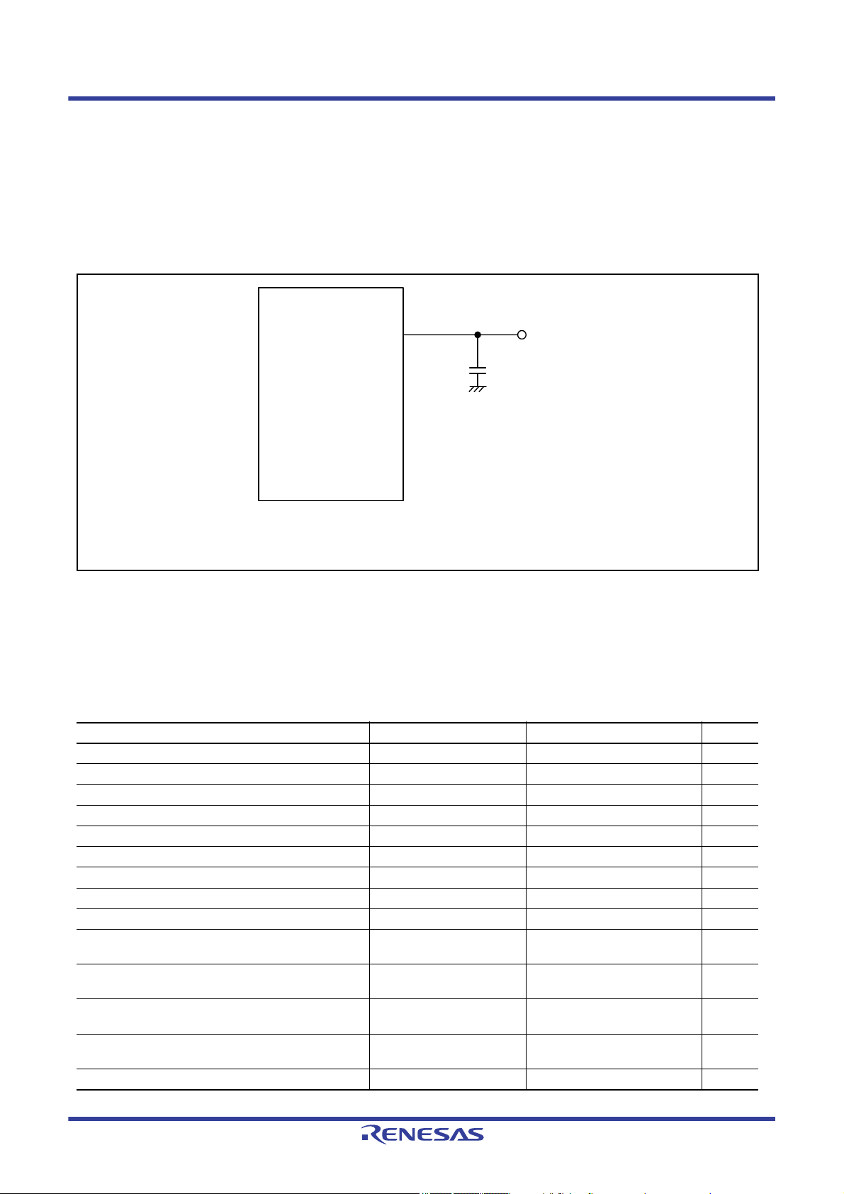
S5D9 Datasheet 2. Electrical Characteristics
For example P100
C
VOH = VCC × 0.7, VOL = VCC × 0.3
V
IH
= VCC × 0.7, VIL = VCC × 0.3
Load capacitance C = 30pF
2. Electrical Characteristics
Unless otherwise specified, the electrical characteristics of the MCU are defined under the following conditions:
VCC = AVCC0 = VCC_USB = VBATT = 2.7 to 3.6 V, 2.7 ≤ VREFH0/VREFH ≤ AVCC0, VCC_USBHS =
AVCC_USBHS = 3.0 to 3.6 V, VSS = AVSS0 = VREFL0/VREFL = VSS_USB = VSS1_USBHS = VSS2_USBHS =
PVSS_USBHS = AVSS_USBHS = 0 V, Ta = Topr.
Figure 2.1 shows the timing conditions.
Figure 2.1 Input or output timing measurement conditions
The measurement conditions of timing specification in each peripherals are recommended for the best peripheral
operation, however make sure to adjust driving abilities of each pins to meet your conditions.
2.1 Absolute Maximum Ratings
Table 2.1 Absolute maximum ratings
Parameter Symbol Value Unit
Power supply voltage VCC, VCC_USB *
VBATT power supply voltage VBATT -0.3 to +4.0 V
1
Input voltage (except for 5V-tolerant ports*
1
Input voltage (5V-tolerant ports*
Reference power supply voltage VREFH/VREFH0 -0.3 to AVCC0 + 0.3 V
Analog power supply voltage AVCC0 *
USBHS power supply voltage VCC_USBHS -0.3 to +4.0 V
USBHS analog power supply voltage AVCC_USBHS -0.3 to +4.0 V
Analog input voltage (except for P000 to P007) V
Analog input voltage (P000 to P007) when PGA
differential input is disabled
Analog input voltage (P000 to P002, P004 to P006)
when PGA differential input is enabled
Analog input voltage (P003, P007) when PGA
differential input is enabled
Operating temperature*
Storage temperature T
3,*4,*5
)Vin-0.3 to + VCC + 4.0 (max 5.8) V
)V
in
2
AN
V
AN
V
AN
V
AN
T
opr
stg
2
-0.3 to +4.0 V
-0.3 to VCC + 0.3 V
-0.3 to +4.0 V
-0.3 to AVCC0 + 0.3 V
-0.3 to AVCC0 + 0.3 V
-1.3 to AVCC0 + 0.3 V
-0.8 to AVCC0 + 0.3 V
-40 to +85
-40 to +105
-55 to +125 °C
°C
R01DS0303EU0130 Rev.1.30 Page 28 of 116
Aug 30, 2019
Page 29
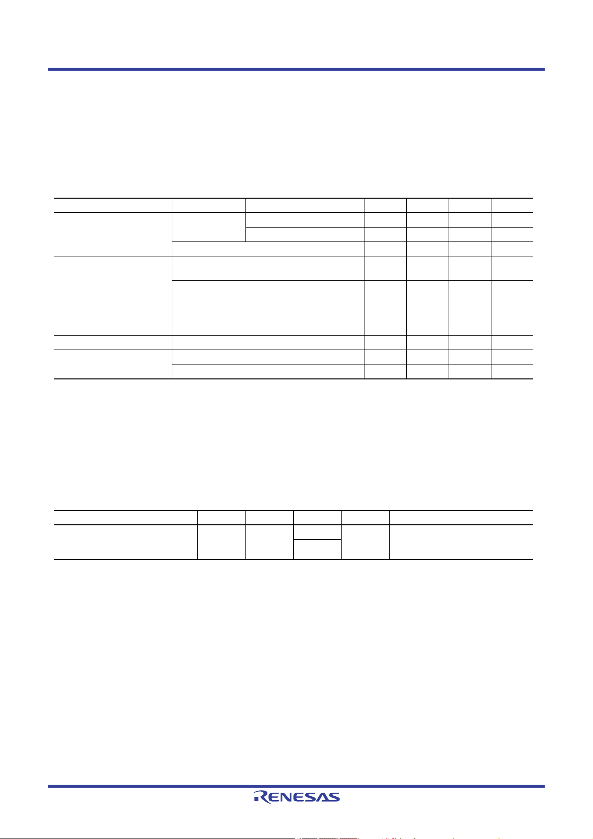
S5D9 Datasheet 2. Electrical Characteristics
Caution: Permanent damage to the MCU might result if absolute maximum ratings are exceeded.
Note 1. Ports P205, P206, P400, P401, P407 to P415, P511, P512, P708 to P713, and PB01 are 5V-tolerant.
Note 2. Connect AVCC0 and VCC_USB to VCC.
Note 3. See section 2.2.1, T
Note 4. Contact a Renesas Electronics sales office for information on derating operation when T
systematic reduction of load for improved reliability.
Note 5. The upper limit of operating temperature is 85°C or 105°C, depending on the product. For details, see section 1.3, Part
Numbering.
Table 2.2 Recommended operating conditions
Parameter Symbol Value Min Typ Max Unit
Power supply voltages VCC When USB/SDRAM is not used 2.7 - 3.6 V
USB power supply voltages VCC_USB,
VBATT power supply voltage VBATT 1.8 - 3.6 V
Analog power supply voltages AVCC0*
Definition.
j/Ta
When USB/SDRAM is used 3.0 - 3.6 V
VSS -0-V
VCC_USBHS
VSS_USB,
AVSS_USBHS,
PVSS_USBHS,
VSS1_USBHS,
VSS2_USBHS
1
AVSS0 - 0 - V
-VCC-V
-0-V
-VCC-V
= +85°C to +105°C. Derating is the
a
Note 1. Connect AVCC0 to VCC. When neither the A/D converter nor the D/A converter nor the comparator is in use, do not leave the
AVCC0, VREFH/VREFH0, AVSS0, and VREFL/VREFL0 pins open. Connect the AVCC0 and VREFH/VREFH0 pins to VCC,
and the AVSS0 and VREFL/VREFL0 pins to VSS, respectively.
2.2 DC Characteristics
2.2.1 Tj/Ta Definition
Table 2.3 DC characteristics
Conditions: Products with operating temperature (Ta) -40 to +105°C
Parameter Symbol Typ Max Unit Test conditions
Permissible junction temperature T
Note: Make sure that Tj = Ta + θja × total power consumption (W), where total power consumption = (VCC - VOH) × ΣIOH + VOL × ΣIOL
max × VCC.
+ I
Note 1. The upper limit of operating temperature is 85°C or 105°C, depending on the product. For details, see section 1.3, Part
CC
Numbering. If the part number shows the operation temperature to 85°C, then Tj max is 105°C, otherwise, 125°C.
j
- 125 °C High-speed mode
1
105*
Low-speed mode
Subosc-speed mode
R01DS0303EU0130 Rev.1.30 Page 29 of 116
Aug 30, 2019
Page 30
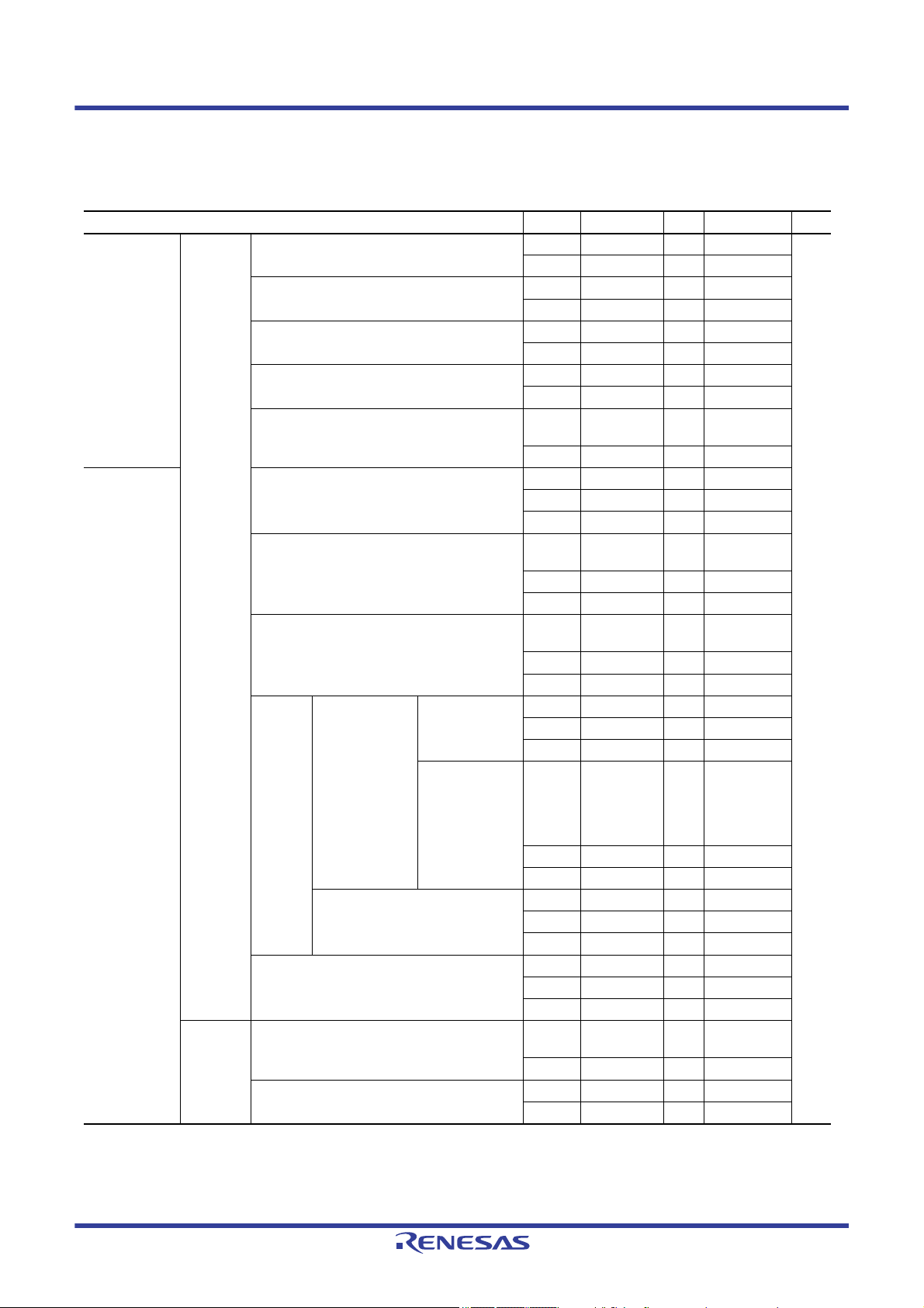
S5D9 Datasheet 2. Electrical Characteristics
2.2.2 I/O VIH, V
Table 2.4 I/O VIH, V
IL
IL
Parameter Symbol Min Typ Max Unit
Input voltage
(except for
Schmitt trigger
input pins)
Schmitt trigger
input voltage
Peripheral
function
pin
EXTAL(external clock input), WAIT, SPI (except
RSPCK)
D00 to D15,
DQ00 to DQ15
ETHERC V
IIC (SMBus)*
IIC (SMBus)*
IIC (except for SMBus)*
IIC (except for SMBus)*
5V-tolerant ports*
1
2
1
2
3, *7
V
V
V
V
V
V
V
V
V
V
V
ΔV
V
V
ΔV
V
IH
IL
IH
IL
IH
IL
IH
IL
IH
IL
IH
IL
IH
IL
IH
VCC × 0.8 - - V
- - VCC × 0.2
VCC × 0.7 - -
- - VCC × 0.3
2.3 - -
- - VCC × 0.2
2.1 - -
--0.8
2.1 - VCC + 3.6
(max 5.8)
--0.8
VCC × 0.7 - -
- - VCC × 0.3
VCC × 0.05 - -
T
VCC × 0.7 - VCC + 3.6
(max 5.8)
- - VCC × 0.3
VCC × 0.05 - -
T
VCC × 0.8 - VCC + 3.6
(max 5.8)
RTCIC0,
RTCIC1,
RTCIC2
When using the
Battery Backup
Function
When VBATT
power supply is
selected
When VCC
power supply is
selected
V
ΔV
V
V
ΔV
V
IL
IH
IL
IH
- - VCC × 0.2
VCC × 0.05 - -
T
V
× 0.8 - V
BATT
--V
V
T
× 0.05 - -
BATT
VCC × 0.8 - Higher
+ 0.3
BATT
× 0.2
BATT
voltage either
VCC + 0.3 V
or
V
+ 0.3 V
BATT
When not using the Battery Backup
Function
Other input pins*
Ports 5V-tolerant ports*
Other input pins*
4
5, *7
6
V
ΔV
V
V
ΔV
V
V
ΔV
V
V
V
V
IL
IH
IL
IH
IL
IH
IL
IH
IL
- - VCC × 0.2
VCC × 0.05 - -
T
VCC × 0.8 - VCC + 0.3
- - VCC × 0.2
VCC × 0.05 - -
T
VCC × 0.8 - -
- - VCC × 0.2
VCC × 0.05 - -
T
VCC × 0.8 - VCC + 3.6
- - VCC × 0.2
VCC × 0.8 - -
- - VCC × 0.2
(max 5.8)
Note 1. SCL0_B (P204), SCL1_B, SDA1_B (total 3 pins).
Note 2. SCL0_A, SDA0_A, SCL0_B (P408), SDA0_B, SCL1_A, SDA1_A, SCL2, SDA2 (total 8 pins).
Note 3. RES and peripheral function pins associated with P205, P206, P400, P401, P407 to P415, P511, P512, P708 to P713, PB01
(total 23 pins).
R01DS0303EU0130 Rev.1.30 Page 30 of 116
Aug 30, 2019
Page 31

S5D9 Datasheet 2. Electrical Characteristics
Note 4. All input pins except for the peripheral function pins already described in the table.
Note 5. P205, P206, P400, P401, P407 to P415, P511, P512, P708 to P713, PB01 (total 22 pins).
Note 6. All input pins except for the ports already described in the table.
Note 7. When VCC is less than 2.7 V, the input voltage of 5 V-tolerant ports should be less than 3.6 V, otherwise breakdown might
occur because the 5 V-tolerant ports are electrically controlled to not violate the breakdown voltage.
2.2.3 I/O IOH, I
Table 2.5 I/O IOH, I
OL
OL
Parameter Symbol Min Typ Max Unit
Permissible output current
(average value per pin)
Permissible output current
(max value per pin)
Permissible output current
(max value total pins)
Ports P008 to P010, P201 - I
Ports P014, P015 - I
Ports P205, P206, P407 to P415,
P602, P708 to P713, PB01 (total
19 pins)
Other output pins
Ports P008 to P010, P201 - I
Ports P014, P015 - I
Ports P205, P206, P407 to P415,
P602, P708 to P713, PB01
(total 19 pins)
Other output pins
Maximum of all output pins ΣI
4
*
4
*
Low drive
Middle drive
High drive
Low drive*
Middle drive
High drive
Low drive
Middle drive
High drive
Low drive*
Middle drive
High drive
1
*
2
*
3
*
1
2
*
3
*
1
*
2
*
3
*
1
2
*
3
*
OH
I
OL
OH
I
OL
I
OH
I
OL
I
OH
I
OL
I
OH
I
OL
I
OH
I
OL
I
OH
I
OL
I
OH
I
OL
OH
I
OL
OH
I
OL
I
OH
I
OL
I
OH
I
OL
I
OH
I
OL
I
OH
I
OL
I
OH
I
OL
I
OH
I
OL
OH (max)
ΣI
OL (max)
----2.0mA
--2.0mA
---4.0mA
--4.0mA
---2.0mA
--2.0mA
---4.0mA
--4.0mA
---20mA
--20mA
---2.0mA
--2.0mA
---4.0mA
--4.0mA
---16mA
--16mA
---4.0mA
--4.0mA
---8.0mA
--8.0mA
---4.0mA
--4.0mA
---8.0mA
--8.0mA
---40mA
--40mA
---4.0mA
--4.0mA
---8.0mA
--8.0mA
---32mA
--32mA
---80mA
--80mA
Caution: To protect the reliability of the MCU, the output current values should not exceed the values in this
table. The average output current indicates the average value of current measured during 100 μs.
Note 1. This is the value when low driving ability is selected in the port drive capability bit in the PmnPFS register. The selected driving
ability is retained in Deep Software Standby mode.
Note 2. This is the value when middle driving ability is selected in the port drive capability bit in the PmnPFS register. The selected
driving ability is retained in Deep Software Standby mode.
Note 3. This is the value when high driving ability is selected in the port drive capability bit in the PmnPFS register. The selected driving
ability is retained in Deep Software Standby mode.
R01DS0303EU0130 Rev.1.30 Page 31 of 116
Aug 30, 2019
Page 32

S5D9 Datasheet 2. Electrical Characteristics
Note 4. Except for P000 to P007, P200, which are input ports.
2.2.4 I/O VOH, VOL, and Other Characteristics
Table 2.6 I/O VOH, VOL, and other characteristics
ParameterParameter Symbol Min Typ Max Unit Test conditions
Output voltage IIC V
1
IIC
*
ETHERC V
Ports P205, P206, P407 to P415,
P602, P708 to P713, PB01 (total 19
2
*
pins)
Other output pins V
Input leakage current RES |I
Ports P000 to P002, P004 to P006,
P200
Ports P003, P007 Before
Three-state leakage
current (off state)
Input pull-up MOS current Ports P0 to PB (except for ports
Input capacitance USB_DP, USB_DM, and ports
5V-tolerant ports |I
Other ports (except for ports P000
to P007, P200)
P000 to P007)
P003, P007, P014, P015, P400,
P401, P511, P512
Other input pins - - 8
initialization*
After
initialization*
3
4
OL
V
OL
V
OL
V
OL
OH
V
OL
V
OH
V
OL
OH
V
OL
|- -5.0μAV
in
|- -5.0μAV
TSI
I
p
C
in
--0.4VI
--0.6 I
--0.4 I
-0.4- I
VCC - 0.5 - - IOH = -1.0 mA
--0.4 I
VCC - 1.0 - - IOH = -20 mA
--1.0 I
VCC - 0.5 - - IOH = -1.0 mA
--0.5 I
--1.0 V
--45.0 V
--1.0 V
--1.0 V
-300 - -10 μA VCC = 2.7 to 3.6 V
- - 16 pF Vbias = 0V
= 3.0 mA
OL
= 6.0 mA
OL
= 15.0 mA
OL
(ICFER.FMPE = 1)
= 20.0 mA
OL
(ICFER.FMPE = 1)
= 1.0 mA
OL
VCC = 3.3 V
= 20 mA
OL
VCC = 3.3 V
= 1.0 mA
OL
= 0 V
in
= 5.5 V
V
in
= 0 V
in
= VCC
V
in
= 0 V
in
= VCC
V
in
= 0 V
in
= VCC
V
in
= 0 V
in
= 5.5 V
V
in
= 0 V
in
V
= VCC
in
= 0 V
V
in
Vam p = 20m V
f = 1 MHz
= 25°C
T
a
Note 1. SCL0_A, SDA0_A (total 2 pins).
Note 2. This is the value when high driving ability is selected in the port drive capability bit in the PmnPFS register.
The selected driving ability is retained in Deep Software Standby mode.
Note 3. P0nPFS.ASEL (n = 3 or 7) = 1.
Note 4. P0nPFS.ASEL (n = 3 or 7) = 0.
R01DS0303EU0130 Rev.1.30 Page 32 of 116
Aug 30, 2019
Page 33

S5D9 Datasheet 2. Electrical Characteristics
2.2.5 Operating and Standby Current
Table 2.7 Operating and standby current (1 of 2)
Parameter Symbol Min Typ Max Unit Test conditions
Supply
1
current
*
Analog
power
supply
current
Reference
power
supply
current
(VREFH0)
Reference
power
supply
current
(VREFH)
Maximum*
CoreMark®
Normal mode All peripheral clocks enabled,
Sleep mode
Increase during BGO
operation
High-speed mode
Low-speed mode
Subosc-speed mode
Software Standby mode - 1.8 18 Ta
Power supplied to Standby SRAM and USB resume
detecting unit
Power not supplied to
SRAM or USB resume
detecting unit
Increase when the RTC
and AGT are operating
Deep Software Standby mode
RTC operating while VCC is off (with
the battery backup function, only the
RTC and sub-clock oscillator
operate)
During 12-bit A/D conversion AI
During 12-bit A/D conversion with S/H amp - 2.3 3.3 mA -
PGA (1ch) - 1 3 mA -
ACMPHS (1unit) - 100 150 µA -
Temperature sensor - 0.1 0.2 mA -
During D/A conversion (per unit) Without AMP output - 0.1 0.2 mA -
Waiting for A/D, D/A conversion (all units) - 0.9 1.6 mA -
ADC12, DAC12 in standby modes (all units)*
During 12-bit A/D conversion (unit 0) AI
Waiting for 12-bit A/D conversion (unit 0) - 0.07 0.5 μA -
ADC12 in standby modes (unit 0) - 0.07 0.5 µA -
During 12-bit A/D conversion (unit 1) AI
During D/A conversion
(per unit)
Waiting for 12-bit A/D (unit 1), D/A (all units) conversion - 0.070.8 µA -
ADC12 unit 1 in standby modes - 0.07 0.8 µA -
2
5
*
while (1) code executing from
4
flash
*
All peripheral clocks disabled,
while (1) code executing from
5, *6
flash
*
5, *6
*
Data flash P/E - 6 -
Code flash P/E - 8 -
5
*
5
*
Power-on reset circuit lowpower function disabled
Power-on reset circuit lowpower function enabled
When the low-speed on-chip
oscillator (LOCO) is in use
When a crystal oscillator for
low clock loads is in use
When a crystal oscillator for
standard clock loads is in use
When a crystal
oscillator for low clock
loads is in use
When a crystal
oscillator for standard
clock loads is in use
With AMP output - 0.6 1.1 mA -
8
Without AMP output - 0.1 0.4 mA -
With AMP ouput - 0.1 0.4 mA -
I
CC
3
*
CC
REFH0
REFH
--
-21-
-34-
-14-
-1246
-2.4- ICLK = 1 MHz
- 2 - ICLK = 32.768 kHz
2
mA ICLK = 120 MHz
137
*
PCLKA = 120 MHz*
PCLKB = 60 MHz
PCLKC = 60 MHz
PCLKD = 120 MHz
FCLK = 60 MHz
BCLK = 120 MHz
≤ 85°C
-1.828 Ta
-3079μATa ≤ 85°C
-30113μATa
-1333μATa
-1340 Ta
-6.328 Ta
-6.334 Ta
-5- -
-1.0- -
-1.5- -
-0.9- V
-1.3- V
-1.1- V
-1.8- V
-0.81.1mA-
-28µA-
- 70 120 μA -
- 70 120 µA -
≤ 105°C
≤ 105°C
≤ 85°C
≤ 105°C
≤ 85°C
≤ 105°C
= 1.8 V,
BATT
VCC = 0 V
= 3.3 V,
BATT
VCC = 0 V
= 1.8 V,
BATT
VCC = 0 V
= 3.3 V,
BATT
VCC = 0 V
7
R01DS0303EU0130 Rev.1.30 Page 33 of 116
Aug 30, 2019
Page 34

S5D9 Datasheet 2. Electrical Characteristics
Table 2.7 Operating and standby current (2 of 2)
Parameter Symbol Min Typ Max Unit Test conditions
USB
operating
current
Note 1. Supply current values are with all output pins unloaded and all input pull-up MOS transistors in the off state.
Note 2. Measured with clocks supplied to the peripheral functions. This does not include the BGO operation.
Note 3. ICC depends on f (ICLK) as follows. (ICLK:PCLKA:PCLKB:PCLKC:PCLKD:BCK:EBCLK = 2:2:1:1:2:1:1)
Note 4. This does not include the BGO operation.
Note 5. Supply of the clock signal to peripherals is stopped in this state. This does not include the BGO operation.
Note 6. FCLK, BCLK, PCLKA, PCLKB, PCLKC, and PCLKD are set to divided by 64 (3.75 MHz).
Note 7. When using ETHERC, GLCDC, DRW, and JPEG, PCLKA frequency is such that PCLKA = ICLK.
Note 8. When the MCU is in Software Standby mode or the MSTPCRD.MSTPD16 (ADC120 Module Stop bit) and
Low speed USB I
USBHS - 10.5 13.5 mA VCC_USBHS =
USBHS - 2.8 3.6 mA VCC_USBHS =
Full speed USB I
USBHS - 14 22 mA VCC_USBHS =
USBHS - 6.5 13.0 mA VCC_USBHS =
High speed USBHS I
Standby mode (direct power down) USBHS I
CCUSBLS
CCUSBFS
CCUSBHS
CCUSBSBY
- 3.5 6.5 mA VCC_USB
AVCC_USBHS
(PHYSET.HSEB = 0)
AVCC_USBHS
(PHYSET.HSEB = 1)
- 4.0 10.0 mA VCC_USB
AVCC_USBHS
(PHYSET.HSEB = 0)
AVCC_USBHS
(PHYSET.HSEB = 1)
- 50 65 mA VCC_USBHS =
- 0.5 4.5 μA VCC_USBHS =
AVCC_USBHS
AVCC_USBHS
ICC Max. = 0.84 × f + 37 (max. operation in High-speed mode)
ICC Typ. = 0.09 × f + 3.7 (normal operation in High-speed mode)
ICC Typ. = 0.6 × f + 1.8 (Low-speed mode 1)
ICC Max. = 0.08 × f + 37 (Sleep mode).
MSTPCRD.MSTPD15 (ADC121 Module Stop bit) are in the module-stop state. See section 47.6.8, Available Functions and
Register Settings of AN000 to AN002, AN007, AN100 to AN102, and AN107 in User’s Manual.
R01DS0303EU0130 Rev.1.30 Page 34 of 116
Aug 30, 2019
Page 35

S5D9 Datasheet 2. Electrical Characteristics
1
10
100
-40 -20 0 20 40 60 80 100
ICC (mA)
Ta (Ԩ)
Average value of the tested middle samples during product evaluation.
Average value of the tested upper -limit samples during product eval uation.
1
10
100
1000
-40-20 0 20406080100
ICC (uA)
Ta (Ԩ)
Average value of the tested middle samples during product evaluatio n.
Average value of the tested upper-limit samples during product e valuation.
Figure 2.2 Temperature dependency in Software Standby mode (reference data)
Figure 2.3 Temperature dependency in Deep Software Standby mode, power supplied to standby SRAM and
USB resume detecting unit (reference data)
R01DS0303EU0130 Rev.1.30 Page 35 of 116
Aug 30, 2019
Page 36

S5D9 Datasheet 2. Electrical Characteristics
1
10
100
-40-20 0 20406080100
ICC (uA)
Ta (Ԩ)
Average value of the tested middle samples during product evaluation.
Average value of the tested upper-limit samples during product evaluation.
1
10
100
-40-20 0 20406080100
ICC (uA)
Ta (Ԩ)
Average value of the tested middle samples during product evaluation.
Average value of the tested upper-limit samples during product evaluation.
Figure 2.4 Temperature dependency in Deep Software Standby mode, power not supplied to SRAM or USB
resume detecting unit, power-on reset circuit low-power function disabled (reference data)
Figure 2.5 Temperature dependency in Deep Software Standby mode, power not supplied to SRAM or USB
R01DS0303EU0130 Rev.1.30 Page 36 of 116
Aug 30, 2019
resume detecting unit, power-on reset circuit low-power function enabled (reference data)
Page 37

S5D9 Datasheet 2. Electrical Characteristics
V
r(VCC)
VCC
1/f
r(VCC)
2.2.6 VCC Rise and Fall Gradient and Ripple Frequency
Table 2.8 Rise and fall gradient characteristics
Parameter Symbol Min Typ Max Unit Test conditions
VCC rising gradient Voltage monitor 0 reset disabled at startup SrVCC 0.0084 - 20 ms/V -
Voltage monitor 0 reset enabled at startup 0.0084 - - -
1
SfVCC 0.0084 - - ms/V -
VCC falling gradient*
SCI/USB boot mode*
2
Note 1. At boot mode, the reset from voltage monitor 0 is disabled regardless of the value of OFS1.LVDAS bit.
Note 2. This applies when VBATT is used.
Table 2.9 Rise and fall gradient and ripple frequency characteristics
The ripple voltage must meet the allowable ripple frequency f
(2.7 V). When the VCC change exceeds VCC ±10%, the allowable voltage change rising and falling gradient dt/dVCC must be met.
Parameter Symbol Min Typ Max Unit Test conditions
Allowable ripple frequency f
r (VCC)
--10kHzFigure 2.6
--1MHzFigure 2.6
--10MHzFigure 2.6
Allowable voltage change rising
dt/dVCC 1.0 - - ms/V When VCC change exceeds VCC ±10%
and falling gradient
within the range between the VCC upper limit (3.6 V) and lower limit
r(VCC)
0.0084 - 20 -
V
≤ VCC × 0.2
r (VCC)
V
≤ VCC × 0.08
r (VCC)
V
≤ VCC × 0.06
r (VCC)
Figure 2.6 Ripple waveform
2.3 AC Characteristics
2.3.1 Frequency
Table 2.10 Operation frequency value in high-speed mode
Parameter Symbol Min Typ Max Unit
Operation frequency System clock (ICLK*
Peripheral module clock (PCLKA)*
Peripheral module clock (PCLKB)*
Peripheral module clock (PCLKC)*
Peripheral module clock (PCLKD)*
Flash interface clock (FCLK)*
External bus clock (BCLK)*
EBCLK pin output - - 60
SDCLK pin output VCC ≥ 3.0 V - - 120
R01DS0303EU0130 Rev.1.30 Page 37 of 116
Aug 30, 2019
2
) f - - 120 MHz
2
2
2
2
2
2
- - 120
--60
3
-*
-60
- - 120
1
-*
-60
- - 120
Page 38

S5D9 Datasheet 2. Electrical Characteristics
Note 1. FCLK must run at a frequency of at least 4 MHz when programming or erasing the flash memory.
Note 2. See section 9, Clock Generation Circuit in User’s Manual for the relationship between the ICLK, PCLKA, PCLKB, PCLKC,
PCLKD, FCLK, and BCLK frequencies.
Note 3. When the ADC12 is used, the PCLKC frequency must be at least 1 MHz.
Table 2.11 Operation frequency value in low-speed mode
Parameter Symbol Min Typ Max Unit
Operation frequency System clock (ICLK)*
Peripheral module clock (PCLKA)*
Peripheral module clock (PCLKB)*
Peripheral module clock (PCLKC)*
Peripheral module clock (PCLKD)*
Flash interface clock (FCLK)*
External bus clock (BCLK) - - 1
EBCLK pin output - - 1
Note 1. Programming or erasing the flash memory is disabled in low-speed mode.
Note 2. See section 9, Clock Generation Circuit in User’s Manual for the relationship between the ICLK, PCLKA, PCLKB, PCLKC,
PCLKD, FCLK, and BCLK frequencies.
Note 3. When the ADC12 is used, the PCLKC frequency must be set to at least 1 MHz.
2
2
2
2,*3
2
1, *2
f--1MHz
--1
--1
3
-*
-1
--1
--1
Table 2.12 Operation frequency value in Subosc-speed mode
Parameter Symbol Min Typ Max Unit
Operation frequency System clock (ICLK)*
Peripheral module clock (PCLKA)*
Peripheral module clock (PCLKB)*
Peripheral module clock (PCLKC)*
Peripheral module clock (PCLKD)*
Flash interface clock (FCLK)*
External bus clock (BCLK)*
2
2
2
2,*3
2
1, *2
2
f 27.8 - 37.7 kHz
- - 37.7
- - 37.7
- - 37.7
- - 37.7
27.8 - 37.7
- - 37.7
EBCLK pin output - - 37.7
Note 1. Programming or erasing the flash memory is disable in Subosc-speed mode.
Note 2. See section 9, Clock Generation Circuit in User’s Manual for the relationship between the ICLK, PCLKA, PCLKB, PCLKC,
PCLKD, FCLK, and BCLK frequencies.
Note 3. The ADC12 cannot be used.
2.3.2 Clock Timing
Table 2.13 Clock timing except for sub-clock oscillator (1 of 2)
Parameter Symbol Min Typ Max Unit Test conditions
EBCLK pin output cycle time t
EBCLK pin output high pulse width t
EBCLK pin output low pulse width t
EBCLK pin output rise time t
EBCLK pin output fall time t
SDCLK pin output cycle time t
SDCLK pin output high pulse width t
SDCLK pin output low pulse width t
SDCLK pin output rise time t
SDCLK pin output fall time t
Bcyc
CH
CL
Cr
Cf
SDcyc
CH
CL
Cr
Cf
16.6 - - ns Figure 2.7
3.3 - - ns
3.3 - - ns
--5.0ns
--5.0ns
8.33 - - ns
1.0 - - ns
1.0 - - ns
--3.0ns
--3.0ns
R01DS0303EU0130 Rev.1.30 Page 38 of 116
Aug 30, 2019
Page 39

S5D9 Datasheet 2. Electrical Characteristics
Table 2.13 Clock timing except for sub-clock oscillator (2 of 2)
Parameter Symbol Min Typ Max Unit Test conditions
EXTAL external clock input cycle time t
EXTAL external clock input high pulse width t
EXTAL external clock input low pulse width t
EXTAL external clock rise time t
EXTAL external clock fall time t
Main clock oscillator frequency f
Main clock oscillation stabilization wait time
(crystal) *
1
LOCO clock oscillation frequency f
LOCO clock oscillation stabilization wait time t
ILOCO clock oscillation frequency f
MOCO clock oscillation frequency F
MOCO clock oscillation stabilization wait time t
HOCO clock oscillator
Without FLL f
oscillation frequency
With FLL f
HOCO clock oscillation stabilization wait time*
2
FLL stabilization wait time t
PLL clock frequency f
PLL clock oscillation stabilization wait time t
EXcyc
EXH
EXL
EXr
EXf
MAIN
t
MAINOSCWT
LOCO
LOCOWT
ILOCO
MOCO
MOCOWT
HOCO16
f
HOCO18
f
HOCO20
f
HOCO16
f
HOCO18
f
HOCO20
HOCO16
f
HOCO18
f
HOCO20
t
HOCOWT
FLLWT
PLL
PLLWT
41.66 - - ns Figure 2.8
15.83 - - ns
15.83 - - ns
--5.0ns
--5.0ns
8-24MHz-
---*1ms Figure 2.9
27.8528 32.768 37.6832 kHz -
- - 60.4 μs Figure 2.10
12.75 15 17.25 kHz -
6.8 8 9.2 MHz -
- - 15.0 μs-
15.78 16 16.22 MHz -20 ≤ Ta ≤ 105°C
17.75 18 18.25
19.72 20 20.28
15.71 16 16.29 -40 ≤ Ta ≤ -20°C
17.68 18 18.32
19.64 20 20.36
15.955 16 16.045 -40 ≤ Ta ≤ 105°C
17.949 18 18.051
19.944 20 20.056
Sub-clock
frequency accuracy
is ±50 ppm.
- - 64.7 μs-
--1.8ms-
120 - 240 MHz -
- - 174.9 μs Figure 2.11
Note 1. When setting up the main clock oscillator, ask the oscillator manufacturer for an oscillation evaluation and use the results as the
recommended oscillation stabilization time. Set the MOSCWTCR register to a value equal to or greater than the recommended
value.
After changing the setting in the MOSCCR.MOSTP bit to start main clock operation, read the OSCSF.MOSCSF flag to confirm
that it is 1, and then start using the main clock oscillator.
Note 2. This is the time from release from reset state until the HOCO oscillation frequency (fHOCO) reaches the range for guaranteed
operation.
Table 2.14 Clock timing for the sub-clock oscillator
Parameter Symbol Min Typ Max Unit Test conditions
Sub-clock frequency f
Sub-clock oscillation stabilization wait time t
SUB
SUBOSCWT
Note 1. When setting up the sub-clock oscillator, ask the oscillator manufacturer for an oscillation evaluation and use the results as the
recommended oscillation stabilization time.
After changing the setting in the SOSCCR.SOSTP bit to start sub-clock operation, only start using the sub-clock oscillator after
the sub-clock oscillation stabilization time elapses with an adequate margin. Two times the value shown is recommended.
- 32.768 - kHz -
--*1s Figure 2.12
R01DS0303EU0130 Rev.1.30 Page 39 of 116
Aug 30, 2019
Page 40

S5D9 Datasheet 2. Electrical Characteristics
t
Cf
t
CH
t
Bcyc
, t
SDcyc
t
Cr
t
CL
EBCLK pin output, SDCLK pin output
t
EXH
t
EXcyc
EXTAL external clock input
VCC × 0.5
t
EXL
t
EXr
t
EXf
Main clock oscillator output
MOSCCR.MOSTP
Main clock
t
MAINOSCWT
LOCO clock
LOCOCR.LCSTP
t
LOCOWT
On-chip oscillator output
Figure 2.7 EBCLK and SDCLK output timing
Figure 2.8 EXTAL external clock input timing
Figure 2.9 Main clock oscillation start timing
Figure 2.10 LOCO clock oscillation start timing
R01DS0303EU0130 Rev.1.30 Page 40 of 116
Aug 30, 2019
Page 41

S5D9 Datasheet 2. Electrical Characteristics
PLLCR.PLLSTP
OSCSF.PLLSF
PLL clock
t
PLLWT
PLL circuit output
Sub-clock oscillator output
SOSCCR.SOSTP
t
S UBO SC
Sub-clock
Figure 2.11 PLL clock oscillation start timing
Note: Only operate the PLL is operated after main clock oscillation has stabilized.
Figure 2.12 Sub-clock oscillation start timing
2.3.3 Reset Timing
Table 2.15 Reset timing
Parameter Symbol Min Typ Max Unit
RES pulse width Power-on t
Deep Software Standby mode t
Software Standby mode, Subosc-speed
mode
All other t
Wait time after RES cancellation t
Wait time after internal reset cancellation
(IWDT reset, WDT reset, software reset, SRAM parity error
reset, SRAM ECC error reset, bus master MPU error reset, bus
slave MPU error reset, stack pointer error reset)
RESWP
RESWD
t
RESWS
RESW
RESWT
t
RESW2
1- - msFigure 2.13
0.6 - - ms Figure 2.14
0.3 - - ms
200 - - μs
-2933μsFigure 2.13
- 320 408 μs -
Test
conditions
R01DS0303EU0130 Rev.1.30 Page 41 of 116
Aug 30, 2019
Page 42

S5D9 Datasheet 2. Electrical Characteristics
VCC
RES
Internal reset signal
(low is valid)
t
RESWP
t
RESWT
RES
Internal reset signal
(low is valid)
t
RESWD
, t
RESWS
, t
RESW
t
RESWT
Figure 2.13 Power-on reset timing
Figure 2.14 Reset input timing
2.3.4 Wakeup Timing
Table 2.16 Timing of recovery from low power modes
Parameter Symbol Min Typ Max Unit
Recovery time
from Software
Standby mode*
1
Crystal
resonator
connected
to main
clock
System clock source is main
clock oscillator*
System clock source is PLL
with main clock oscillator*
2
3
oscillator
External
clock input
to main
clock
oscillator
System clock source is main
clock oscillator*
4
System clock source is PLL
with main clock oscillator*
5
System clock source is sub-clock
oscillator*
System clock source is LOCO*
System clock source is HOCO clock
oscillator*
System clock source is MOCO clock
oscillator*
8
8
6
7
Recovery time from Deep Software Standby mode t
Wait time after cancellation of Deep Software Standby mode t
Recovery time
from Software
Standby mode to
Snooze mode
High-speed mode when system clock
source is HOCO (20 MHz)
High-speed mode when system clock
source is MOCO (8 MHz)
t
SBYMC
t
SBYPC
t
SBYEX
t
SBYPE
t
SBYSC
t
SBYLO
t
SBYHO
t
SBYMO
DSBY
DSBYWT
t
SNZ
t
SNZ
- 2.4*
- 2.7*
- 230*
- 570*
9
9
9
9
-1.2*91.3*
-1.2*91.4*
- 240*9, *10310
- 220*
9
- 0.65 1.0 ms Figure 2.16
34 - 35 t
- 35*9, *
10
-11*914*9 μs
9
2.8*
9
3.2*
280*9μs
700*9μs
9
9
9, *10
*
9
300*
71
9, *10
*
Test
conditions
ms Figure 2.15
The division
ms
ratio of all
oscillators is
1.
ms
ms
µs
µs
cyc
μs Figure 2.17
R01DS0303EU0130 Rev.1.30 Page 42 of 116
Aug 30, 2019
Page 43

S5D9 Datasheet 2. Electrical Characteristics
Note 1. The recovery time is determined by the system clock source. When multiple oscillators are active, the recovery time can be
determined with the following equation:
Total recovery time = recovery time for an oscillator as the system clock source + the longest oscillation stabilization time of any
oscillators requiring longer stabilization times than the system clock source + 2 LOCO cycles (when LOCO is operating) + 3
SOSC cycles (when Subosc is oscillating and MSTPC0 = 0 (CAC module stop)).
Note 2. When the frequency of the crystal is 24 MHz (Main Clock Oscillator Wait Control Register (MOSCWTCR) is set to 05h). For
other settings (MOSCWTCR is set to Xh), the recovery time can be determined with the following equation:
t
(MOSCWTCR = Xh) = t
SBYMC
(MOSCWTCR = 05h) + (t
SBYMC
MAINOSCWT
(MOSCWTCR = Xh) - t
MAINOSCWT
(MOSCWTCR =
05h))
Note 3. When the frequency of PLL is 240 MHz (Main Clock Oscillator Wait Control Register (MOSCWTCR) is set to 05h). For other
settings (MOSCWTCR is set to Xh), the recovery time can be determined with the following equation:
t
(MOSCWTCR = Xh) = t
SBYMC
(MOSCWTCR = 05h) + (t
SBYMC
MAINOSCWT
(MOSCWTCR = Xh) - t
MAINOSCWT
(MOSCWTCR =
05h))
Note 4. When the frequency of the external clock is 24 MHz (Main Clock Oscillator Wait Control Register (MOSCWTCR) is set to 00h).
For other settings (MOSCWTCR is set to Xh), the recovery time can be determined with the following equation:
t
(MOSCWTCR = Xh) = t
SBYMC
(MOSCWTCR = 00h) + (t
SBYMC
MAINOSCWT
(MOSCWTCR = Xh) - t
MAINOSCWT
(MOSCWTCR =
00h))
Note 5. When the frequency of PLL is 240 MHz (Main Clock Oscillator Wait Control Register (MOSCWTCR) is set to 00h). For other
settings (MOSCWTCR is set to Xh), the recovery time can be determined with the following equation:
t
(MOSCWTCR = Xh) = t
SBYMC
(MOSCWTCR = 00h) + (t
SBYMC
MAINOSCWT
(MOSCWTCR = Xh) - t
MAINOSCWT
(MOSCWTCR =
00h))
Note 6. The HOCO frequency is 20 MHz.
Note 7. The MOCO frequency is 8 MHz.
Note 8. In Subosc-speed mode, the sub-clock oscillator or LOCO continues oscillating in Software Standby mode.
Note 9. When the SNZCR.RXDREQEN bit is set to 0, the following time is added as the power supply recovery time:
STCONR.STCON[1:0] = 00b:16 µs (typical), 34 µs (maximum)
STCONR.STCON[1:0] = 11b:16 µs (typical), 104 µs (maximum).
Note 10. When the SNZCR.RXDREQEN bit is set to 0, 16 μs (typical) or 18 μs (maximum) is added as the HOCO wait time.
R01DS0303EU0130 Rev.1.30 Page 43 of 116
Aug 30, 2019
Page 44

S5D9 Datasheet 2. Electrical Characteristics
Oscillator
(syste m clock)
ICLK
IRQ
Software Standby mode
t
SBYMC, tSBYEX, tSBYPC, tSBYPE,
t
SBYPH, tSBYSC, tSBYHO, tSBYLO
Oscillator
(not the system clock)
t
SBYOSCWTtSBYSEQ
Oscillator
(system clock)
ICLK
IRQ
Software Standby mode
t
SBYMC, tSBYEX, tSBYPC, tSBYPE,
t
SBYPH, tSBYSC, tSBYHO, tSBYLO
t
SBYOSCWT
t
SBYOSCWT
When stabilization of the system clock oscillator is slower
t
SBYSEQ
Oscillator
(not the system clock)
When stabilization of an oscillator other than the system clock is slower
Figure 2.15 Software Standby mode cancellation timing
R01DS0303EU0130 Rev.1.30 Page 44 of 116
Aug 30, 2019
Page 45

S5D9 Datasheet 2. Electrical Characteristics
Oscillator
IRQ
Internal reset
(low is valid)
Reset exception handling start
Deep Software Standby mode
Deep Software Standby
reset
(low is valid)
t
DSBY
t
DSBYWT
t
SNZ
IRQ
ICLK(to DTC, SRAM)
*1
PCLK
ICLK(except DTC, SRAM)
Oscillator
Software Standby mode Snooze mode
Note 1. When SNZCR.SNZDTCEN is set to 1, ICLK is supplied to DTC and SRAM.
Figure 2.16 Deep Software Standby mode cancellation timing
Figure 2.17 Recovery timing from Software Standby mode to Snooze mode
2.3.5 NMI and IRQ Noise Filter
Table 2.17 NMI and IRQ noise filter
Parameter Symbol Min Typ Max Unit Test conditions
NMI pulse width t
IRQ pulse width t
Note: 200 ns minimum in Software Standby mode.
Note: If the clock source is switched, add 4 clock cycles of the switched source.
R01DS0303EU0130 Rev.1.30 Page 45 of 116
Aug 30, 2019
NMIW
200 - - ns NMI digital filter disabled t
1
t
Pcyc
× 2*
-- t
200 - - NMI digital filter enabled t
2
IRQW
× 3.5*
t
NMICK
200 - - ns IRQ digital filter disabled t
1
× 2*
t
Pcyc
-- t
-- t
200 - - IRQ digital filter enabled t
3
× 3.5*
t
IRQCK
-- t
× 2 ≤ 200 ns
Pcyc
× 2 > 200 ns
Pcyc
× 3 ≤ 200 ns
NMICK
× 3 > 200 ns
NMICK
× 2 ≤ 200 ns
Pcyc
× 2 > 200 ns
Pcyc
× 3 ≤ 200 ns
IRQCK
× 3 > 200 ns
IRQCK
Page 46

S5D9 Datasheet 2. Electrical Characteristics
t
NMIW
NMI
t
IRQW
IRQ
Note 1. t
Note 2. t
Note 3. t
indicates the PCLKB cycle.
Pcyc
indicates the cycle of the NMI digital filter sampling clock.
NMICK
indicates the cycle of the IRQi digital filter sampling clock.
IRQCK
Figure 2.18 NMI interrupt input timing
Figure 2.19 IRQ interrupt input timing
2.3.6 Bus Timing
Table 2.18 Bus timing (1 of 2)
Condition 1: When using the CS area controller (CSC).
BCLK = 8 to 120 MHz, EBCLK = 8 to 60 MHz
VCC = AVCC0 = VCC_USB = VBATT = 2.7 to 3.6 V, VREFH/VREFH0 = 2.7 V to AVCC0,
VCC_USBHS = AVCC_USBHS = 3.0 to 3.6 V
Output load conditions: VOH = VCC × 0.5, VOL = VCC × 0.5, C = 30 pF
EBCLK: High drive output is selected in the port drive capability bit in the PmnPFS register.
Others: Middle drive output is selected in the port drive capability bit in the PmnPFS register.
Condition 2: When using the SDRAM area controller (SDRAMC).
BCLK = SDCLK = 8 to 120 MHz
VCC = AVCC0 = VCC_USB = VBATT = 3.0 to 3.6 V, VREFH/VREFH0 = 3.0 V to AVCC0,
VCC_USBHS = AVCC_USBHS = 3.0 to 3.6 V
Output load conditions: VOH = VCC × 0.5, VOL = VCC × 0.5, C = 15 pF
High drive output is selected in the port drive capability bit in the PmnPFS register.
Condition 3: When using the SDRAM area controller (SDRAMC) and CS area controller (CSC) simultaneously.
BCLK = SDCLK = 8 to 60 MHz
VCC = AVCC0 = VCC_USB = VBATT = 3.0 to 3.6 V, VREFH/VREFH0 = 3.0 V to AVCC0,
VCC_USBHS = AVCC_USBHS = 3.0 to 3.6 V
Output load conditions: VOH = VCC × 0.5, VOL = VCC × 0.5, C = 15 pF
High drive output is selected in the port drive capability bit in the PmnPFS register.
Parameter Symbol Min Max Unit Test conditions
Address delay t
Byte control delay t
CS delay t
ALE delay time t
RD delay t
Read data setup time t
Read data hold time t
WR/WRn delay t
Write data delay t
Write data hold time t
WAIT setup time t
WAIT hold time t
AD
BCD
CSD
ALED
RSD
RDS
RDH
WRD
WDD
WDH
WTS
WTH
- 12.5 ns Figure 2.20 to
- 12.5 ns
Figure 2.25
- 12.5 ns
- 12.5 ns
- 12.5 ns
12.5 - ns
0- ns
- 12.5 ns
- 12.5 ns
0- ns
12.5 - ns Figure 2.26
0- ns
R01DS0303EU0130 Rev.1.30 Page 46 of 116
Aug 30, 2019
Page 47

S5D9 Datasheet 2. Electrical Characteristics
Table 2.18 Bus timing (2 of 2)
Condition 1: When using the CS area controller (CSC).
BCLK = 8 to 120 MHz, EBCLK = 8 to 60 MHz
VCC = AVCC0 = VCC_USB = VBATT = 2.7 to 3.6 V, VREFH/VREFH0 = 2.7 V to AVCC0,
VCC_USBHS = AVCC_USBHS = 3.0 to 3.6 V
Output load conditions: VOH = VCC × 0.5, VOL = VCC × 0.5, C = 30 pF
EBCLK: High drive output is selected in the port drive capability bit in the PmnPFS register.
Others: Middle drive output is selected in the port drive capability bit in the PmnPFS register.
Condition 2: When using the SDRAM area controller (SDRAMC).
BCLK = SDCLK = 8 to 120 MHz
VCC = AVCC0 = VCC_USB = VBATT = 3.0 to 3.6 V, VREFH/VREFH0 = 3.0 V to AVCC0,
VCC_USBHS = AVCC_USBHS = 3.0 to 3.6 V
Output load conditions: VOH = VCC × 0.5, VOL = VCC × 0.5, C = 15 pF
High drive output is selected in the port drive capability bit in the PmnPFS register.
Condition 3: When using the SDRAM area controller (SDRAMC) and CS area controller (CSC) simultaneously.
BCLK = SDCLK = 8 to 60 MHz
VCC = AVCC0 = VCC_USB = VBATT = 3.0 to 3.6 V, VREFH/VREFH0 = 3.0 V to AVCC0,
VCC_USBHS = AVCC_USBHS = 3.0 to 3.6 V
Output load conditions: VOH = VCC × 0.5, VOL = VCC × 0.5, C = 15 pF
High drive output is selected in the port drive capability bit in the PmnPFS register.
Parameter Symbol Min Max Unit Test conditions
Address delay 2 (SDRAM) t
CS delay 2 (SDRAM) t
DQM delay (SDRAM) t
CKE delay (SDRAM) t
Read data setup time 2 (SDRAM) t
Read data hold time 2 (SDRAM) t
Write data delay 2 (SDRAM) t
Write data hold time 2 (SDRAM) t
WE delay (SDRAM) t
RAS delay (SDRAM) t
CAS delay (SDRAM) t
AD2
CSD2
DQMD
CKED
RDS2
RDH2
WDD2
WDH2
WED
RASD
CASD
0.8 6.8 ns Figure 2.27 to
0.8 6.8 ns
Figure 2.33
0.8 6.8 ns
0.8 6.8 ns
2.9 - ns
1.5 - ns
- 6.8 ns
0.8 - ns
0.8 6.8 ns
0.8 6.8 ns
0.8 6.8 ns
R01DS0303EU0130 Rev.1.30 Page 47 of 116
Aug 30, 2019
Page 48

S5D9 Datasheet 2. Electrical Characteristics
Address bus/
data bus
Data read
(RD)
t
AD
EBCLK
Address bus
Address latch
(ALE)
Chip select
(CSn)
t
ALED
T
W1
T
W2
T
n1
t
AD
t
AD
t
RDS
T
n2
t
RSD
t
RSD
T
W3
T
W4
T
W5
T
end
T
a1
T
a1
T
an
Address cycle Data cycle
t
RDH
t
ALED
t
CSD
t
CSD
Address bus/
data bus
Data write
(WRm)
t
AD
EBCLK
Address bus
Address latch
(ALE)
Chip select
(CSn)
t
ALED
T
W1
T
W2
T
n1
t
AD
t
AD
T
n2
t
WRD
t
WRD
T
W3
T
W4
T
W5
T
end
T
a1
T
a1
T
an
Address cycle
Data cycle
t
ALED
t
CSD
t
CSD
t
WDD
t
WDH
T
n3
Figure 2.20 Address/data multiplexed bus read access timing
Figure 2.21 Address/data multiplexed bus write access timing
R01DS0303EU0130 Rev.1.30 Page 48 of 116
Aug 30, 2019
Page 49

S5D9 Datasheet 2. Electrical Characteristics
A23 to A01
CS7 to CS0
t
AD
EBCLK
A2 3 to A00
D15 to D00 (read)
Byte strobe mode
1-write strobe mode
BC1, BC0
Common to both byte strobe mode
and 1-write strobe mode
t
BCD
t
CSD
t
CSD
RD (read)
t
RSD
t
RSD
t
AD
t
RDH
t
RDS
t
AD
t
AD
t
BCD
T
W1
T
W2
T
end
T
n1
T
n2
RDON:1
CSRWAIT: 2
CSROFF: 2
CSON: 0
Figure 2.22 External bus timing for normal read cycle with bus clock synchronized
R01DS0303EU0130 Rev.1.30 Page 49 of 116
Aug 30, 2019
Page 50

S5D9 Datasheet 2. Electrical Characteristics
Note 1. Always specify WDON and WDOFF as at least one EBCLK cycle.
A23 to A01
CS7 to CS0
t
AD
EBCLK
A23 to A00
Byte strobe mode
1-write strobe mode
BC1, BC0
Common to both byte strobe mode
and 1-write strobe mode
t
BCD
t
CSD
t
CSD
t
AD
t
AD
t
AD
t
BCD
D15 to D00 (write)
WR1, WR0, WR (write )
t
WRD
t
WRD
t
WDH
t
WDD
T
W1
T
W2
T
end
T
n1
T
n2
WRON: 1
WDON: 1 *
1
CSWWAIT: 2
WDOFF: 1 *
1
CSON:0
CSWOFF: 2
Figure 2.23 External bus timing for normal write cycle with bus clock synchronized
R01DS0303EU0130 Rev.1.30 Page 50 of 116
Aug 30, 2019
Page 51

S5D9 Datasheet 2. Electrical Characteristics
A23 t o A01
CS7 to CS0
t
AD
EBCLK
A23 t o A00
D15 to D00 (Read)
Byte strobe mode
1-write strobe mode
BC1, BC0
Common to both byte strobe mode
and 1-write strobe mod e
t
BCD
t
CSD
t
CSD
RD (Read)
t
RSD
t
RSD
t
RDH
t
RDS
t
AD
t
BCD
T
W1TW2
T
endTpw1
T
pw2
t
AD
t
AD
t
RSD
t
RSD
t
RDH
t
RDS
t
RSD
t
RSD
t
RDH
t
RDS
T
end
T
pw1
T
pw2
T
end
T
n1
T
n2
t
AD
t
AD
t
AD
t
AD
RDON:1
CSRWAIT:2
CSROFF:2
t
RSD
t
RSD
t
RDH
t
RDS
t
AD
t
AD
CSPRWAIT:2
T
pw1
T
pw2
T
end
RDON:1
CSPRWAIT:2
RDON:1
CSPRWAIT: 2
RDON:1
CSON:0
Note 1. Always specify WDON and WDOFF as at least one EBCLK cycle.
A23 to A01
CS7 to CS0
t
AD
EBCLK
A23 to A0 0
Byte s trobe mode
1-wri te strobe mode
BC1, BC0
Comm on to both byte strobe m ode
and 1-w rite strobe m ode
t
BCD
t
CSD
t
CSD
t
AD
t
BCD
T
W1
D15 to D00 (wr ite)
WR1, WR0, W R (write)
t
WRD
t
WRD
t
WDH
t
WDD
T
W2
T
end
T
pw1
T
pw2
t
AD
t
AD
t
WRD
t
WRD
t
WDH
t
WDD
t
WRD
t
WRD
t
WDH
t
WDD
T
dw1 T
end
T
pw1
T
pw2 T
end
T
n1
T
n2
T
dw1
t
AD
t
AD
t
AD
t
AD
WRON:1
WDON:1*
1
CSWW AIT:2
CSPW WAIT:2
WDOFF:1*
1
CSPW WAIT:2
WDOFF:1*
1
WDOFF:1*
1
CSON:0
WRON:1
WDON:1*
1
WRON:1
WDON:1*
1
CSWOFF:2
Figure 2.24 External bus timing for page read cycle with bus clock synchronized
Figure 2.25 External bus timing for page write cycle with bus clock synchronized
R01DS0303EU0130 Rev.1.30 Page 51 of 116
Aug 30, 2019
Page 52

S5D9 Datasheet 2. Electrical Characteristics
t
WTStWTH
t
WTStWTH
CSRWAIT:3
CSWWA IT:3
EBCLK
A23 to A00
CS7 to CS0
RD (read)
WR (write)
WAIT
T
W1
T
W2
(T
end
)T
end
T
W3
T
n1
T
n2
External wait
Figure 2.26 External bus timing for external wait control
R01DS0303EU0130 Rev.1.30 Page 52 of 116
Aug 30, 2019
Page 53

S5D9 Datasheet 2. Electrical Characteristics
Note 1. Address pins are for output of the precharge-select command (Precharge-sel) for the SDRAM.
t
AD2
SDCLK
A15 to A00
SDCS
AP*
1
DQMn
DQ15 to DQ00
RAS
CAS
WE
CKE
t
DQMD
(High)
Row
address
Column address
SDRAM command ACT RD PRA
t
AD2
t
CSD2
t
RASD
t
AD2
t
AD2
t
CSD2
t
RASD
t
AD2
t
AD2
t
CSD2
t
RASD
t
AD2
t
AD2
t
CSD2
t
RASD
t
WED
t
WED
t
CSD2
t
CSD2
t
CASD
t
CASD
t
RDS2tRDH2
PRA
command
Figure 2.27 SDRAM single read timing
R01DS0303EU0130 Rev.1.30 Page 53 of 116
Aug 30, 2019
Page 54

S5D9 Datasheet 2. Electrical Characteristics
Note 1. Address pins are for output of the precharge-select command (Precharge-sel) for the SDRAM.
t
AD2
SDCLK
A15 to A00
SDCS
AP*
1
DQMn
DQ15 to DQ00
RAS
CAS
WE
CKE
t
DQMD
(High)
Row
address
Column address
SDRAM command ACT WR PRA
t
AD2
t
CSD2
t
RASD
t
WED
t
CASD
t
WDD2
t
AD2
t
AD2
t
CSD2
t
RASD
t
AD2
t
AD2
t
CSD2
t
RASD
t
AD2
t
AD2
t
CSD2
t
RASD
t
CSD2
t
CSD2
t
CASD
t
WED
t
WED
t
WED
t
WDH2
PRA
comma nd
Figure 2.28 SDRAM single write timing
R01DS0303EU0130 Rev.1.30 Page 54 of 116
Aug 30, 2019
Page 55

S5D9 Datasheet 2. Electrical Characteristics
Note 1. Address pins are for output of the precharge-select command (Precharge-sel) for the SDRAM.
SDCLK
ACT RD RD RD RD PRA
A15 to A00
t
AD2tAD2
t
AD2
t
AD2tAD2tAD2tAD2
t
AD2
AP*
1
SDCS
RAS
CAS
WE
CKE
DQMn
DQ15 to DQ00
C1 C2 C3
Row
address
C0
(column addres s)
t
AD2tAD2
t
AD2tAD2
t
AD2
t
CSD2tCSD2tCSD2
t
CSD2
t
CSD2
t
RASDtRASD
t
RASDtRASD
t
RASD
t
CASD
t
CASD
t
CASD
t
WEDtWED
(High)
t
DQMD
t
DQMD
t
RDS2tRDH2
t
RDS2
t
RDH2
PRA
command
Figure 2.29 SDRAM multiple read timing
R01DS0303EU0130 Rev.1.30 Page 55 of 116
Aug 30, 2019
Page 56

S5D9 Datasheet 2. Electrical Characteristics
Note 1. Address pins are for output of the precharge-select command (Precharge-sel) for the SDRAM.
ACT
WR
PRAWR WR WR
SDCLK
A15 to A00
AP*
1
SDCS
RAS
CAS
WE
CKE
DQMn
DQ15 to DQ00
t
AD2tAD2
t
AD2tAD2tAD2
t
AD2tAD2tAD2
t
AD2
t
AD2
t
AD2tAD2
t
AD2
t
CSD2tCSD2tCSD2
t
CSD2tCSD2
t
RASDtRASD
t
RASDtRASDtRASD
t
CASD
t
CASD t
CASD
t
WED
t
WED
(High)
t
DQMD
t
DQMD
t
WDD2tWDH2
t
WDD2tWDH2
C1 C2 C3
Row
addres s
C0
(c olumn ad dres s)
PRA
command
Figure 2.30 SDRAM multiple write timing
R01DS0303EU0130 Rev.1.30 Page 56 of 116
Aug 30, 2019
Page 57

S5D9 Datasheet 2. Electrical Characteristics
Note 1. Address pins are for output of the precharge-select command (Precharge-sel) for the SDRAM.
R1
A15 to A00
SDCLK
SDCS
AP*
1
DQMn
DQ15 to DQ00
RAS
CAS
WE
CKE
SDRAM command
ACT RDRDRDRDPRA ACT RD RDRDRDPRA
t
CASD
t
RASD
t
CSD2
t
AD2
t
AD2
t
AD2
t
AD2
t
AD2
t
AD2
t
AD2
t
AD2
t
AD2
t
AD2
t
AD2
t
AD2
t
AD2 tAD2
t
AD2 tAD2
t
AD2 tAD2 tAD2 tAD2
t
AD2 tAD2
t
CSD2tCSD2
t
CSD2tCSD2tCSD2tCSD2
t
CSD2
t
RASD
t
RASDtRASDtRASDtRASD
t
CASD
t
CASD
t
RASDtRASD
t
CASD
t
DQMD
t
RDS2tRDH2
t
RDS2tRDH2
t
RDS2tRDH2
t
RDS2tRDH2
(High)
Row
addressC0(column address 0)
C1 C2 C3 C4 C5 C6 C7
PRA
command
PRA
command
t
WEDtWED
t
WEDtWED
Figure 2.31 SDRAM multiple read line stride timing
R01DS0303EU0130 Rev.1.30 Page 57 of 116
Aug 30, 2019
Page 58

S5D9 Datasheet 2. Electrical Characteristics
Note 1. Address pins are for output of the precharge-select command (Precharge-sel) for the SDRAM.
A15 to A00
SDCLK
SDCS
AP*
1
DQMn
DQ15 to DQ00
RAS
CAS
WE
CKE
SDRAM command
(Hi- Z)
(High)
t
CASD
t
RASD
t
CSD2
t
AD2
MRS
t
AD2
t
AD2
t
AD2
t
CASD
t
RASD
t
CSD2
t
WED
t
WED
Figure 2.32 SDRAM mode register set timing
R01DS0303EU0130 Rev.1.30 Page 58 of 116
Aug 30, 2019
Page 59

S5D9 Datasheet 2. Electrical Characteristics
Note 1. Address pins are for output of the precharge-select command (Precharge-sel) for the SDRAM.
A15 to A00
(RFS)
SDCLK
SDCS
AP*
1
DQMn
DQ15 to DQ00
RAS
CAS
WE
CKE
(Hi-Z)
t
CKED
(High)
t
CASD
t
CASD
t
CASD
t
RASDtRASD
t
RASD
t
CSD2
t
CSD2
t
CSD2
t
AD2
t
AD2
(RFA)Ts (RFX) (RFA)
t
AD2
t
AD2
t
CSD2
t
CSD2
t
CSD2
t
CSD2
t
RASD
t
RASDtRASDtRASD
t
CASD
t
CASDtCASDtCASD
t
CKED
SDRAM command
t
DQMD
t
DQMD
Figure 2.33 SDRAM self-refresh timing
2.3.7 I/O Ports, POEG, GPT32, AGT, KINT, and ADC12 Trigger Timing
Table 2.19 I/O ports, POEG, GPT32, AGT, KINT, and ADC12 trigger timing (1 of 2)
GPT32 Conditions:
High drive output is selected in the port drive capability bit in the PmnPFS register.
AGT Conditions:
Middle drive output is selected in the port drive capability bit in the PmnPFS register.
Parameter Symbol Min Max Unit
I/O ports Input data pulse width t
POEG POEG input trigger pulse width t
PRW
POEW
1.5 - t
3- t
Pcyc
Pcyc
Test
conditions
Figure 2.34
Figure 2.35
R01DS0303EU0130 Rev.1.30 Page 59 of 116
Aug 30, 2019
Page 60

S5D9 Datasheet 2. Electrical Characteristics
Port
t
PRW
POEG input trigger
t
POEW
Table 2.19 I/O ports, POEG, GPT32, AGT, KINT, and ADC12 trigger timing (2 of 2)
GPT32 Conditions:
High drive output is selected in the port drive capability bit in the PmnPFS register.
AGT Conditions:
Middle drive output is selected in the port drive capability bit in the PmnPFS register.
Test
Parameter Symbol Min Max Unit
GPT32 Input capture pulse width Single edge t
GTICW
1.5 - t
PDcyc
Dual edge 2.5 -
GTIOCxY output skew
(x = 0 to 7, Y= A or B)
GTIOCxY output skew
(x = 8 to 13, Y = A or B)
GTIOCxY output skew
(x = 0 to 13, Y = A or B)
OPS output skew
GTOUUP, GTOULO, GTOVUP,
Middle drive buffer t
*1-4nsFigure 2.37
GTISK
High drive buffer - 4
Middle drive buffer - 4
High drive buffer - 4
Middle drive buffer - 6
High drive buffer - 6
t
GTOSK
-5nsFigure 2.38
GTOVLO, GTOWUP, GTOWLO
GPT(PWM
Delay
GTIOCxY_Z output skew
(x = 0 to 3, Y = A or B, Z = A)
*2-2.0nsFigure 2.39
t
HRSK
Generation
Circuit)
AGT AGTIO, AGTEE input cycle t
AGTIO, AGTEE input high width, low width t
AGTIO, AGTO, AGTOA, AGTOB output cycle t
ADC12 ADC12 trigger input pulse width t
*3100 - ns Figure 2.40
ACYC
,
ACKWH
t
ACKWL
ACYC2
TRGW
40 - ns
62.5 - ns
1.5 - t
Pcyc
conditions
Figure 2.36
Figure 2.41
KINT KRn (n = 00 to 07) pulse width t
Note: t
: PCLKB cycle, t
Pcyc
: PCLKD cycle.
PDcyc
KR
250 - ns Figure 2.42
Note 1. This skew applies when the same driver I/O is used. If the I/O of the middle and high drivers is mixed, operation is not
guaranteed.
Note 2. The load is 30 pF.
Note 3. Constraints on input:
When not switching the source clock: t
When switching the source clock: t
Pcyc
× 2 < t
Pcyc
× 6 < t
should be satisfied.
ACYC
should be satisfied.
ACYC
Figure 2.34 I/O ports input timing
Figure 2.35 POEG input trigger timing
R01DS0303EU0130 Rev.1.30 Page 60 of 116
Aug 30, 2019
Page 61

S5D9 Datasheet 2. Electrical Characteristics
Inpu t capture
t
GTICW
GPT32 output
PCLKD
t
GTISK
Output delay
GPT32 output
PCLKD
t
GTOSK
Output delay
GPT32 output
(PWM delay
generation circuit)
PCLKD
t
HRSK
Output delay
Figure 2.36 GPT32 input capture timing
Figure 2.37 GPT32 output delay skew
Figure 2.38 GPT32 output delay skew for OPS
Figure 2.39 GPT32 (PWM Delay Generation Circuit) output delay skew
R01DS0303EU0130 Rev.1.30 Page 61 of 116
Aug 30, 2019
Page 62

S5D9 Datasheet 2. Electrical Characteristics
t
ACYC2
AGTIO, AGTEE
(input)
t
ACYC
t
ACKWL
t
ACKWH
AGTIO, AGTO,
AGTOA, AGTOB
(output)
ADTRG0,
ADTRG1
t
TRGW
KR00 to KR07
t
KR
Figure 2.40 AGT input/output timing
Figure 2.41 ADC12 trigger input timing
Figure 2.42 Key interrupt input timing
2.3.8 PWM Delay Generation Circuit Timing
Table 2.20 PWM Delay Generation Circuit timing
Parameter Min Typ Max Unit Test conditions
Operation frequency 80 - 120 MHz -
Resolution - 260 - ps PCLKD = 120 MHz
1
DNL*
Note 1. This value normalizes the differences between lines in 1-LSB resolution.
2.3.9 CAC Timing
Table 2.21 CAC timing
Parameter Symbol Min Typ Max Unit
CAC CACREF input pulse width t
- ±2.0 - LSB -
2
PBcyc
t
PBcyc
≤ tcac*
> tcac*
t
CACREF
2
4.5 × t
5 × t
cac
+ 6.5 × t
cac
+ 3 × t
PBcyc
PBcyc
--ns-
--ns
Test
conditions
R01DS0303EU0130 Rev.1.30 Page 62 of 116
Aug 30, 2019
Page 63

S5D9 Datasheet 2. Electrical Characteristics
t
SCKW
t
SCKr
t
SCKf
t
Scyc
SCKn
(n = 0 to 9)
Note 1. t
Note 2. t
: PCLKB cycle.
PBcyc
: CAC count clock source cycle.
cac
2.3.10 SCI Timing
Table 2.22 SCI timing (1)
Conditions: High drive output is selected in the port drive capability bit in the PmnPFS register for the following pins: SCK0 to SCK9.
For other pins, middle drive output is selected in the port drive capability bit in the PmnPFS register.
Test
*1
Parameter Symbol Min Max Unit
SCI Input clock cycle Asynchronous t
Clock
Scyc
4 - t
6-
Pcyc
synchronous
Input clock pulse width t
Input clock rise time t
Input clock fall time t
Output clock cycle Asynchronous t
Clock
SCKW
SCKr
SCKf
Scyc
0.4 0.6 t
Scyc
-5ns
-5ns
6-t
Pcyc
4-
synchronous
Output clock pulse width t
Output clock rise time t
Output clock fall time t
Transmit data delay Clock
synchronous
Receive data setup time Clock
SCKW
SCKr
SCKf
t
TXD
t
RXS
0.4 0.6 t
Scyc
-5ns
-5ns
-25nsFigure 2.44
15 - ns
synchronous
Receive data hold time Clock
t
RXH
5-ns
synchronous
conditions
Figure 2.43
Note 1. t
: PCLKA cycle.
Pcyc
Figure 2.43 SCK clock input/output timing
R01DS0303EU0130 Rev.1.30 Page 63 of 116
Aug 30, 2019
Page 64

S5D9 Datasheet 2. Electrical Characteristics
t
TXD
t
RXStRXH
TxDn
RxDn
SCKn
n = 0 to 9
Figure 2.44 SCI input/output timing in clock synchronous mode
Table 2.23 SCI timing (2)
Conditions: High drive output is selected in the port drive capability bit in the PmnPFS register for the following pins: SCK0 to SCK9.
For other pins, middle drive output is selected in the port drive capability bit in the PmnPFS register.
Test
Parameter Symbol Min Max Unit
Simple
SPI
SCK clock cycle output
(master)
t
SPcyc
4 (PCLKA ≤ 60 MHz)
8 (PCLKA > 60 MHz)
SCK clock cycle input (slave) - 6 (PCLKA ≤ 60 MHz)
65536 t
65536
Pcyc
12 (PCLKA > 60 MHz)
SCK clock high pulse width t
SCK clock low pulse width t
SCK clock rise and fall time t
Data input setup time t
Data input hold time t
SS input setup time t
SS input hold time t
Data output delay t
Data output hold time t
Data rise and fall time t
SS input rise and fall time t
Slave access time t
SPCKWH
SPCKWL
, t
SPCKr
SU
H
LEAD
LAG
OD
OH
, t
Dr
Df
, t
SSLr
SSLf
SA
SPCKf
0.4 0.6 t
0.4 0.6 t
SPcyc
SPcyc
-20ns
33.3 - ns Figure 2.46 to
33.3 - ns
1- t
1- t
SPcyc
SPcyc
- 33.3 ns
-10 - ns
- 16.6 ns
- 16.6 ns
- 4 (PCLKA ≤ 60 MHz)
t
Pcyc
8 (PCLKA > 60 MHz)
Slave output release time t
REL
- 5 (PCLKA ≤ 60 MHz)
t
Pcyc
10 (PCLKA > 60 MHz)
conditions
Figure 2.45
Figure 2.49
Figure 2.49
R01DS0303EU0130 Rev.1.30 Page 64 of 116
Aug 30, 2019
Page 65

S5D9 Datasheet 2. Electrical Characteristics
t
SPCKWH
V
OH
V
OH
V
OL
V
OL
V
OH
V
OH
t
SPCKWL
t
SPCKr
t
SPCKf
V
OL
t
SPcyc
t
SPCKWH
V
IH
V
IH
V
IL
V
IL
V
IH
V
IH
t
SPCKWL
t
SPCKr
t
SPCKf
V
IL
t
SPcyc
V
OH
= 0.7 × VCC, V
OL
= 0.3 × VCC, V
IH
= 0.7 × VCC, V
IL
= 0.3 × VCC
(n = 0 to 9)
SCKn
master select
output
SCKn
slave select input
t
Dr, tDf
t
SUtH
t
OH
t
OD
MSB IN DATA LSB IN MSB IN
MSB OUT DATA LSB OUT IDLE MSB OUT
SCKn
CKPOL = 0
output
SCKn
CKPOL = 1
output
MISOn
input
MOSIn
output
(n = 0 to 9 )
t
SUtH
t
OH
t
OD
MSB IN DATA LSB IN MSB IN
MSB OUT DATA LSB OUT I DLE MSB OUT
SCKn
CKPOL = 1
output
SCKn
CKPOL = 0
output
MISOn
input
MOSIn
output
(n = 0 to 9 )
t
Dr, tDf
Figure 2.45 SCI simple SPI mode clock timing
Figure 2.46 SCI simple SPI mode timing for master when CKPH = 1
Figure 2.47 SCI simple SPI mode timing for master when CKPH = 0
R01DS0303EU0130 Rev.1.30 Page 65 of 116
Aug 30, 2019
Page 66

S5D9 Datasheet 2. Electrical Characteristics
t
Dr, tDf
t
SUtH
t
LEAD
t
TD
t
LAG
t
SA
MSB IN DATA LSB IN MSB IN
MSB OUT DATA LSB OUT MSB IN MSB OUT
t
OH
t
OD
t
REL
SSn
input
SCKn
CKPOL = 0
input
SCKn
CKPOL = 1
input
MISOn
output
MOSIn
input
(n = 0 to 9 )
t
Dr, tDf
t
SA
t
OH
t
LEAD
t
TD
t
LAG
t
H
LSB OUT
(Last data)
DATA MSB OUT
MSB IN DATA LSB IN M SB IN
LSB OUT
t
SU
t
OD
t
REL
MSB OUT
SSn
inp ut
SCKn
CKPOL = 1
inp ut
SCKn
CKPOL = 0
inp ut
MISOn
output
MOSIn
inp ut
(n = 0 to 9 )
Figure 2.48 SCI simple SPI mode timing for slave when CKPH = 1
Figure 2.49 SCI simple SPI mode timing for slave when CKPH = 0
Table 2.24 SCI timing (3) (1 of 2)
Conditions: Middle drive output is selected in the port drive capability bit in the PmnPFS register.
Parameter Symbol Min Max Unit Test conditions
Simple IIC
(Standard mode)
SDA input rise time t
SDA input fall time t
SDA input spike pulse removal time t
Data input setup time t
Data input hold time t
SCL, SDA capacitive load C
Sr
Sf
SP
SDAS
SDAH
b*
1
- 1000 ns Figure 2.50
- 300 ns
0 4 × t
IICcyc
ns
250 - ns
0- ns
- 400 pF
R01DS0303EU0130 Rev.1.30 Page 66 of 116
Aug 30, 2019
Page 67

S5D9 Datasheet 2. Electrical Characteristics
SDAn
SCLn
V
IH
V
IL
P*
1
S*
1
t
Sf
t
Sr
t
SDAH
t
SDAS
t
SP
P*
1
Test conditi ons :
V
IH
= VCC × 0.7, VIL = VCC × 0.3
V
OL
= 0.6 V, IOL= 6 mA
Sr*
1
Note 1. S, P, and Sr indicate the following:
S: Start condition
P: Stop condition
Sr: Restart condition
(n = 0 to 9)
Table 2.24 SCI timing (3) (2 of 2)
Conditions: Middle drive output is selected in the port drive capability bit in the PmnPFS register.
Parameter Symbol Min Max Unit Test conditions
Simple IIC
(Fast mode)
SDA input rise time t
SDA input fall time t
SDA input spike pulse removal time t
Data input setup time t
Data input hold time t
SCL, SDA capacitive load C
Sr
Sf
SP
SDAS
SDAH
b*
- 300 ns Figure 2.50
- 300 ns
0 4 × t
IICcyc
ns
100 - ns
0- ns
1
- 400 pF
Note: t
: IIC internal reference clock (IICφ) cycle.
IICcyc
Note 1. Cb indicates the total capacity of the bus line.
Figure 2.50 SCI simple IIC mode timing
R01DS0303EU0130 Rev.1.30 Page 67 of 116
Aug 30, 2019
Page 68

S5D9 Datasheet 2. Electrical Characteristics
2.3.11 SPI Timing
Table 2.25 SPI timing
Conditions:
For RSPCKA and RSPCKB pins, high drive output is selected with the port drive capability bit in the PmnPFS register.
For other pins, middle drive output is selected in the port drive capability bit in the PmnPFS register.
Parameter Symbol Min Max Unit*1Test conditions*
SPI RSPCK clock cycle Master t
SPcyc
2 (PCLKA 60 MHz)
4 (PCLKA > 60 MHz)
4096 t
Figure 2.51
Pcyc
C = 30 pF
Slave 4 4096
RSPCK clock high
Master t
pulse width
Slave 2 × t
RSPCK clock low pulse
Master t
width
Slave 2 × t
RSPCK clock rise and
fall time
Master t
Slave - 1 µs
Data input setup time Master t
Slave 5 -
Data input hold time Master
(PCLKA division ratio
SPCKWH(tSPcyc
SPCKWL(tSPcyc
SPCKr,
t
SPCKf
SU
t
HF
t
SPCKf
t
SPCKf
-5ns
4-nsFigure 2.52 to
0-ns
) / 2 - 3
Pcyc
- t
) / 2 - 3
Pcyc
SPCKr
SPCKr
-
-
-ns
-
-ns
-
Figure 2.57
C = 30 pF
- t
set to 1/2)
Master
(PCLKA division ratio
t
H
t
Pcyc
-
set to a value other
than 1/2)
Slave t
SSL setup time Master t
Slave 6 x t
SSL hold time Master t
Slave 6 x t
Data output delay Master t
H
LEAD
LAG
OD
20 -
N × t
N × t
SPcyc
Pcyc
SPcyc
Pcyc
- 10*
- 10 *
3
N ×
t
SPcyc
100*
ns
+
3
-ns
4
N ×
t
SPcyc
100*
ns
+
4
-ns
-6.3ns
Slave - 20
Data output hold time Master t
OH
0-ns
Slave 0 -
t
Successive
Master t
transmission delay
Slave 6 × t
MOSI and MISO rise
and fall time
Output t
Input - 1 μs
SSL rise and fall time Output t
Input - 1 μs
Slave access time t
Slave output release time t
TD
Dr, tDf
SSLr,
t
SSLf
SA
REL
+ 2 × t
SPcyc
Pcyc
Pcyc
-5ns
-5ns
-2 x t
-2 x t
8 ×
t
SPcyc
2 × t
+ 28
+ 28
ns
+
Pcyc
ns Figure 2.56 and
Pcyc
Pcyc
Figure 2.57
C = 30
F
P
2
Note 1. t
: PCLKA cycle.
Pcyc
R01DS0303EU0130 Rev.1.30 Page 68 of 116
Aug 30, 2019
Page 69

S5D9 Datasheet 2. Electrical Characteristics
RSPCKn
master select
output
RSPCKn
slave select input
t
SPCKWH
V
OH
V
OH
V
OL
V
OL
V
OH
V
OH
t
SPCKWL
t
SPCKr
t
SPCKf
V
OL
t
SPcyc
t
SPCKWH
V
IH
V
IH
V
IL
V
IL
V
IH
V
IH
t
SPCKWL
t
SPCKr
t
SPCKf
V
IL
t
SPcyc
V
OH
= 0.7 × VCC, V
OL
= 0.3 × VCC, V
IH
= 0.7 × VCC, V
IL
= 0.3 × VCC
SPI
n = A or B
t
Dr, tDf
t
SUtH
t
LEAD
t
TD
t
LAG
t
SSLr, tSSLf
t
OH
t
OD
MSB IN DATA LSB IN MSB IN
MSB OUT DATA LSB OUT IDLE MSB OUT
SSLn0 to
SSLn3
output
RSPCKn
CPOL = 0
output
RSPCKn
CPOL = 1
output
MISOn
input
MOSIn
output
SPI
n = A or B
Note 2. Must use pins that have a letter (“_A”, “_B”) to indicate group membership appended to their name as groups. For the SPI
interface, the AC portion of the electrical characteristics is measured for each group.
Note 3. N is set to an integer from 1 to 8 by the SPCKD register.
Note 4. N is set to an integer from 1 to 8 by the SSLND register.
Figure 2.51 SPI clock timing
Figure 2.52 SPI timing for master when CPHA = 0
R01DS0303EU0130 Rev.1.30 Page 69 of 116
Aug 30, 2019
Page 70

S5D9 Datasheet 2. Electrical Characteristics
SSLn0 to
SSLn3
output
RSPCKn
CPOL = 0
output
RSPCKn
CPOL = 1
output
MISOn
input
MOSIn
output
LSB IN
t
Dr, tDf
t
SU
t
HF
t
LEAD
t
TD
t
LAG
t
SSLr, tSSLf
t
OH
t
OD
MSB IN
MSB OUT DATA LSB OUT IDLE M SB OUT
MSB IN
DATA
t
HF
SPI
n = A or B
t
SUtH
t
LEAD
t
TD
t
LAG
t
SSLr, tSSLf
t
OH
t
OD
MSB IN D ATA LSB IN MSB IN
MSB OUT DATA LSB OUT IDLE MSB OUT
SSLn0 to
SSLn3
output
RSPCKn
CPOL = 0
output
RSPCKn
CPOL = 1
output
MISOn
inp ut
MOSIn
output
SPI
t
Dr, tDf
n = A or B
Figure 2.53 SPI timing for master when CPHA = 0 and the bit rate is set to PCLKA/2
Figure 2.54 SPI timing for master when CPHA = 1
R01DS0303EU0130 Rev.1.30 Page 70 of 116
Aug 30, 2019
Page 71

S5D9 Datasheet 2. Electrical Characteristics
t
SU
t
HF
t
LEAD
t
TD
t
LAG
t
SSLr, tSSLf
t
OH
t
OD
MSB IN DATA LSB IN MSB IN
MS B OUT DA TA LS B OUT IDLE MS B OUT
SSLn0 to
SSLn3
output
RSPCKn
CPOL = 0
output
RSPCKn
CPOL = 1
output
MISOn
input
MOSIn
output
SPI
t
Dr, tDf
t
H
n = A or B
t
Dr, tDf
t
SUtH
t
LEAD
t
TD
t
LAG
t
SA
MSB IN D ATA LS B IN MSB IN
MSB OUT D ATA LSB OUT MSB IN MSB OUT
t
OH
t
OD
t
REL
SSLn0
input
RSPCKn
CPOL = 0
input
RSPCKn
CPOL = 1
input
MISOn
output
MOSIn
input
SPI
n = A or B
Figure 2.55 RSPI timing for master when CPHA = 1 and the bit rate is set to PCLKA/2
Figure 2.56 SPI timing for slave when CPHA = 0
R01DS0303EU0130 Rev.1.30 Page 71 of 116
Aug 30, 2019
Page 72

S5D9 Datasheet 2. Electrical Characteristics
SSLn0
input
RSPCKn
CPOL = 0
input
RSPCKn
CPOL = 1
input
MISOn
output
MOSIn
input
t
Dr, tDf
t
SA
t
OH
t
LEAD
t
TD
t
LAG
t
H
LSB O UT
(Last data)
DATA MSB OUT
MSB IN DATA LSB IN MSB IN
LSB OUT
t
SU
t
OD
t
REL
MSB OUT
SPI
n = A or B
t
QScyc
QSPCLK output
t
QSWH
t
QSWL
Figure 2.57 SPI timing for slave when CPHA = 1
2.3.12 QSPI Timing
Table 2.26 QSPI timing
Conditions: High drive output is selected in the port drive capability bit in the PmnPFS register.
Parameter Symbol Min Max Unit*
QSPI QSPCK clock cycle t
QSPCK clock high pulse width t
QSPCK clock low pulse width t
Data input setup time t
Data input hold time t
QSSL setup time t
QSSL hold time t
Data output delay t
Data output hold time t
Successive transmission delay t
Note 1. t
: PCLKA cycle.
Pcyc
Note 2. N is set to 0 or 1 in SFMSLD.
Note 3. N is set to 0 or 1 in SFMSHD.
QScyc
QSWH
QSWL
Su
IH
LEAD
LAG
OD
OH
TD
248t
t
× 0.4 - ns
QScyc
t
× 0.4 - ns
QScyc
8- nsFigure 2.59
0- ns
(N+0.5) x
t
- 5 *
Qscyc
(N+0.5) x
t
- 5 *
Qscyc
2
3
(N+0.5) x
t
+100 *
Qscyc
(N+0.5) x
t
+100 *
Qscyc
ns
2
ns
3
-4ns
-3.3 - ns
116t
Pcyc
QScyc
1
Test conditions
Figure 2.58
R01DS0303EU0130 Rev.1.30 Page 72 of 116
Aug 30, 2019
Figure 2.58 QSPI clock timing
Page 73

S5D9 Datasheet 2. Electrical Characteristics
t
SUtH
t
LEAD
t
TD
t
LAG
t
OH
t
OD
MSB IN DATA LSB IN
MSB OUT DATA LSB OUT IDLE
QSSL
output
QSPCLK
output
QIO0-3
input
QIO0-3
output
Figure 2.59 Transmit and receive timing
2.3.13 IIC Timing
Table 2.27 IIC timing (1) (1 of 2)
(1) Conditions: Middle drive output is selected in the port drive capability bit in the PmnPFS register for the following pins: SDA0_B,
SCL0_B, SDA1_A, SCL1_A, SDA1_B, SCL1_B.
(2) The following pins do not require setting: SCL0_A, SDA0_A, SCL2, SDA2.
(3) Use pins that have a letter appended to their names, for instance “_A” or “_B”, to indicate group membership. For the IIC interface, the
AC portion of the electrical characteristics is measured for each group.
ns
Test
conditions*
3
Parameter Symbol Min*
IIC
(Standard mode,
SMBus)
ICFER.FMPE = 0
SCL input cycle time t
SCL input high pulse width t
SCL input low pulse width t
SCL, SDA input rise time t
SCL, SDA input fall time t
SCL, SDA input spike pulse removal
SCL
SCLH
SCLL
Sr
Sf
t
SP
6 (12) × t
3 (6) × t
3 (6) × t
- 1000 ns
- 300 ns
0 1 (4) × t
time
SDA input bus free time when
t
BUF
3 (6) × t
wakeup function is disabled
SDA input bus free time when
wakeup function is enabled
START condition input hold time
t
BUF
t
STAH
3 (6) × t
+ 300
t
IICcyc
when wakeup function is disabled
START condition input hold time
when wakeup function is enabled
Repeated START condition input
t
STAH
t
STAS
1 (5) × t
300
1000 - ns
setup time
1000 - ns
0-ns
- 400 pF
STOP condition input setup time t
Data input setup time t
Data input hold time t
SCL, SDA capacitive load C
STOS
SDAStIICcyc
SDAH
b
1
+ 1300 - ns Figure 2.60
IICcyc
+ 300 - ns
IICcyc
+ 300 - ns
IICcyc
+ 300 - ns
IICcyc
+ 4 × t
IICcyc
Max Unit
IICcyc
-ns
Pcyc
+ 300 - ns
+ t
+
IICcyc
Pcyc
-ns
+ 50 - ns
R01DS0303EU0130 Rev.1.30 Page 73 of 116
Aug 30, 2019
Page 74

S5D9 Datasheet 2. Electrical Characteristics
Table 2.27 IIC timing (1) (2 of 2)
(1) Conditions: Middle drive output is selected in the port drive capability bit in the PmnPFS register for the following pins: SDA0_B,
SCL0_B, SDA1_A, SCL1_A, SDA1_B, SCL1_B.
(2) The following pins do not require setting: SCL0_A, SDA0_A, SCL2, SDA2.
(3) Use pins that have a letter appended to their names, for instance “_A” or “_B”, to indicate group membership. For the IIC interface, the
AC portion of the electrical characteristics is measured for each group.
ns
Test
conditions*
3
Parameter Symbol Min*
IIC
(Fast mode)
SCL input cycle time t
SCL input high pulse width t
SCL input low pulse width t
SCL, SDA input rise time t
SCL
SCLH
SCLL
Sr
6 (12) × t
3 (6) × t
3 (6) × t
20 × (external pullup
voltage/5.5V)*
SCL, SDA input fall time t
SCL, SDA input spike pulse removal
time
SDA input bus free time when
wakeup function is disabled
SDA input bus free time when
wakeup function is enabled
START condition input hold time
when wakeup function is disabled
START condition input hold time
when wakeup function is enabled
Repeated START condition input
setup time
STOP condition input setup time t
Data input setup time t
Data input hold time t
SCL, SDA capacitive load C
Sf
t
SP
t
BUF
t
BUF
t
STAH
t
STAH
t
STAS
STOS
SDAStIICcyc
SDAH
b
20 × (external pullup
voltage/5.5V)*
0 1 (4) × t
3 (6) × t
3 (6) × t
+ 300
t
IICcyc
1 (5) × t
300
300 - ns
300 - ns
0-ns
- 400 pF
1
+ 600 - ns Figure 2.60
IICcyc
+ 300 - ns
IICcyc
+ 300 - ns
IICcyc
2
Max Unit
300 ns
300 ns
2
IICcyc
+ 300 - ns
IICcyc
IICcyc
+ 4 × t
-ns
Pcyc
+ 300 - ns
+ t
+
IICcyc
Pcyc
-ns
+ 50 - ns
Note: t
: IIC internal reference clock (IICφ) cycle, t
IICcyc
: PCLKB cycle.
Pcyc
Note 1. Values in parentheses apply when ICMR3.NF[1:0] is set to 11b while the digital filter is enabled with ICFER.NFE set to 1.
Note 2. Only supported for SCL0_A, SDA0_A, SCL2, and SDA2.
Note 3. Must use pins that have a letter (“_A”, “_B”) to indicate group membership appended to their name as groups. For the IIC
interface, the AC portion of the electrical characteristics is measured for each group.
R01DS0303EU0130 Rev.1.30 Page 74 of 116
Aug 30, 2019
Page 75

S5D9 Datasheet 2. Electrical Characteristics
SDA0 to SDA2
SCL0 to SCL2
V
IH
V
IL
t
STAH
t
SCLH
t
SCLL
P*
1
S*
1
t
Sf
t
Sr
t
SCL
t
SDAH
t
SDAS
t
STAS
t
SP
t
STOS
P*
1
t
BUF
Test conditions:
V
IH
= V CC × 0.7 , VIL= VCC × 0.3
V
OL
= 0.6 V, IOL = 6 mA (ICFER.FMPE = 0)
V
OL
= 0.4 V, IOL = 15 mA (IC FE R.F MPE = 1)
Sr*
1
Note 1. S, P , and Sr ind icate th e fol lowing :
S: Start condi tio n
P: Stop conditi on
Sr: Restart condition
Table 2.28 IIC timing (2)
Setting of the SCL0_A, SDA0_A pins is not required with the port drive capability bit in the PmnPFS register.
Test
conditions
ns
Parameter Symbol Min*1,*
IIC
(Fast-mode+)
ICFER.FMPE = 1
SCL input cycle time t
SCL input high pulse width t
SCL input low pulse width t
SCL, SDA input rise time t
SCL, SDA input fall time t
SCL, SDA input spike pulse removal
time
SDA input bus free time when
SCL
SCLH
SCLL
Sr
Sf
t
SP
t
BUF
6 (12) × t
3 (6) × t
3 (6) × t
- 120 ns
- 120 ns
0 1 (4) × t
3 (6) × t
wakeup function is disabled
SDA input bus free time when
wakeup function is enabled
Start condition input hold time when
t
BUF
t
STAH
3 (6) × t
+ 120
t
IICcyc
wakeup function is disabled
START condition input hold time
when wakeup function is enabled
Restart condition input setup time t
Stop condition input setup time t
Data input setup time t
Data input hold time t
SCL, SDA capacitive load C
t
STAH
1 (5) × t
120
STAS
STOS
SDAStIICcyc
SDAH
b
120 - ns
120 - ns
0-ns
- 550 pF
2
+ 240 - ns Figure 2.60
IICcyc
+ 120 - ns
IICcyc
+ 120 - ns
IICcyc
+ 120 - ns
IICcyc
+ 4 × t
IICcyc
Max Unit
IICcyc
-ns
Pcyc
+ 120 - ns
+ t
+
IICcyc
Pcyc
-ns
+ 30 - ns
Note: t
: IIC internal reference clock (IICφ) cycle, t
IICcyc
: PCLKB cycle.
Pcyc
Note 1. Values in parentheses apply when ICMR3.NF[1:0] is set to 11b while the digital filter is enabled with ICFER.NFE set to 1.
Note 2. Cb indicates the total capacity of the bus line.
Figure 2.60 I2C bus interface input/output timing
R01DS0303EU0130 Rev.1.30 Page 75 of 116
Aug 30, 2019
Page 76

S5D9 Datasheet 2. Electrical Characteristics
SSIBCKn
t
HC
tO, t
I
t
LC
t
RC
t
FC
2.3.14 SSIE Timing
Table 2.29 SSIE timing
(1) High drive output is selected with the port drive capability bit in the PmnPFS register.
(2) Use pins that have a letter appended to their names, for instance “_A” or “_B” to indicate group membership. For the SSIE interface,
the AC portion of the electrical characteristics is measured for each group.
Target specification
Parameter Symbol
SSIBCK Cycle Master t
Slave t
High level/ low level Master t
O
I
HC/tLC
80 - ns Figure 2.61
80 - ns
0.35 - t
Slave 0.35 - t
Rising time/falling time Master tRC/t
-0.15t
FC
Slave - 0.15 tO / t
SSILRCK/SSIFS,
SSITXD0, SSIRXD0,
SSIDATA1
Input set up time Master t
Slave 12 - ns
Input hold time Master t
SR
HR
12 - ns Figure 2.63,
8- ns
Slave 15 - ns
Output delay time Master t
DTR
-10 5 ns
Slave 0 20 ns Figure 2.63,
Output delay time from
SSILRCK/SSIFS
Slave t
DTRW
-20nsFigure 2.65*
change
GTIOC1A,
AUDIO_CLK
Cycle t
High level/ low level t
EXcyc
EXL
t
EXH
20 - ns Figure 2.62
/
0.4 0.6 t
Note 1. For slave-mode transmission, SSIE has a path, through which the signal input from the SSILRCK/SSIFS pin is used to
generate transmit data, and the transmit data is logically output to the SSITXD0 or SSIDATA1 pin.
Unit CommentsMin. Max.
O
I
/ t
O
EXcyc
I
I
Figure 2.64
Figure 2.64
1
Figure 2.61 SSIE clock input/output timing
R01DS0303EU0130 Rev.1.30 Page 76 of 116
Aug 30, 2019
Page 77

S5D9 Datasheet 2. Electrical Characteristics
GTIOC1A,
AUDIO_CLK
(input)
t
EXH
t
EXL
t
EXr
t
EXcyc
t
EXf
1/2 VCC
t
SR
t
HR
t
DTR
SSIBCKn
(Input or Output)
SSILRCKn/SSIFSn (input),
SSIRXD0,
SSIDAT A1 (input)
SSILRCKn/SSIFSn (output),
SSITXD0,
SSIDATA1 (output)
Figure 2.62 Clock input timing
Figure 2.63 SSIE data transmit and receive timing when SSICR.BCKP = 0
R01DS0303EU0130 Rev.1.30 Page 77 of 116
Aug 30, 2019
Page 78

S5D9 Datasheet 2. Electrical Characteristics
t
SR
t
HR
t
DTR
SSIBCKn
(Input or Output)
SSILRCKn/SSIFSn (input),
SSIRXD0,
SSIDATA1 (input)
SSILRCKn/SSIFSn (output),
SSITXD0,
SSIDATA1 (output)
t
DTRW
SSILRCKn/SSIFSn(input)
SSITXD0,
SSIDATA1 (output)
MSB bit output delay after SSILRCKn/SSIFSn change for slave
transmitter when DEL = 1, SDTA = 0 or DEL = 1, SDTA = 1, SWL[2:0] = DWL[2:0] in SSICR.
Figure 2.64 SSIE data transmit and receive timing when SSICR.BCKP = 1
Figure 2.65 SSIE data output delay after SSILRCKn/SSIFSn change
2.3.15 SD/MMC Host Interface Timing
Table 2.30 SD/MMC Host Interface signal timing
Conditions: High drive output is selected in the port drive capability bit in the PmnPFS register.
Clock duty ratio is 50%.
Parameter Symbol Min Max Unit Test conditions*
SDCLK clock cycle T
SDCLK clock high pulse width T
SDCLK clock low pulse width T
SDCLK clock rise time T
SDCLK clock fall time T
SDCMD/SDDAT output data delay T
SDCMD/SDDAT input data setup T
SDCMD/SDDAT input data hold T
SDCYC
SDWH
SDWL
SDLH
SDHL
SDODLY
SDIS
SDIH
20 - ns Figure 2.66
6.5 - ns
6.5 - ns
-3ns
-3ns
-6 5 ns
4- ns
2- ns
Note 1. Must use pins that have a letter (“_A”, “_B”) to indicate group membership appended to their name as groups. For
R01DS0303EU0130 Rev.1.30 Page 78 of 116
Aug 30, 2019
1
Page 79

S5D9 Datasheet 2. Electrical Characteristics
SDnCLK
(output)
SDnCMD/SDnDATm
(input)
SDnCMD/SDnDATm
(output)
T
SDOD LY(m ax)
T
SDIS
T
SDIH
T
SDLH
T
SDHL
T
SDCYC
T
SDWH
T
SDWL
T
SDODLY(min)
n = 0, 1 ; m = 0 to 7
Figure 2.66 SD/MMC Host Interface signal timing
2.3.16 ETHERC Timing
Table 2.31 ETHERC timing
Conditions: ETHERC (RMII): Middle drive output is selected in the port drive capability bit in the PmnPFS register for the following pins:
ET0_MDC, ET0_MDIO.
For other pins, high drive output is selected in the port drive capability bit in the PmnPFS register.
ETHERC (MII): Middle drive output is selected in the port drive capability bit in the PmnPFS register.
Parameter Symbol Min Max Unit
ETHERC
(RMII)
ETHERC
(MII)
Note 1. RMII0_TXD_EN, RMII0_TXD1, RMII0_TXD0.
Note 2. RMII0_CRS_DV, RMII0_RXD1, RMII0_RXD0, RMII0_RX_ER.
R01DS0303EU0130 Rev.1.30 Page 79 of 116
Aug 30, 2019
the SD/MMC Host interface, the AC portion of the electrical characteristics is measured for each group.
Test
conditions*
REF50CK cycle time T
ck
REF50CK frequency, typical 50 MHz - - 50 + 100 ppm MHz
REF50CK duty - 35 65 %
REF50CK rise/fall time T
RMII0_xxxx*
RMII0_xxxx*
RMII0_xxxx*
RMII0_xxxx*
1
output delay T
2
setup time T
2
hold time T
1, *2
rise/fall time Tr/T
ET0_WOL output delay t
ET0_TX_CLK cycle time t
ET0_TX_EN output delay t
ET0_ETXD0 to ET0_ETXD3 output delay t
ET0_CRS setup time t
ET0_CRS hold time t
ET0_COL setup time t
ET0_COL hold time t
ET0_RX_CLK cycle time t
ET0_RX_DV setup time t
ET0_RX_DV hold time t
ET0_ERXD0 to ET0_ERXD3 setup time t
ET0_ERXD0 to ET0_ERXD3 hold time t
ET0_RX_ER setup time t
ET0_RX_ER hold time t
ET0_WOL output delay t
ckr/ckf
co
su
hd
WOLd
Tc yc
TENd
MTDd
CRSs
CRSh
COLs
COLh
TRcyc
RDVs
RDVh
MRDs
MRDh
RERs
RESh
WOLd
20 - ns Figure 2.67 to
0.5 3.5 ns
2.5 12.0 ns
3- ns
1- ns
0.5 4 ns
f
1 23.5 ns Figure 2.71
40 - ns -
120nsFigure 2.72
120ns
10 - ns
10 - ns
10 - ns Figure 2.73
10 - ns
40 - ns -
10 - ns Figure 2.74
10 - ns
10 - ns
10 - ns
10 - ns Figure 2.75
10 - ns
1 23.5 ns Figure 2.76
Figure 2.70
3
Page 80

S5D9 Datasheet 2. Electrical Characteristics
Note 1. RMII0_TXD_EN, RMII0_TXD1, RMII0_TXD0, RMII0_CRS_DV, RMII0_RXD1, RMII0_RXD0,
RMII0_RX_ER
Change in
signal level
Signal
ThdTsuTco
TfTr
Tckr
Tckf
Tck
Signal
90%
50%
10%
90%
50%
REF50C K0
RMII0 _xxxx
*1
10%
Change
in signal
level
Change
in signal
level
Preamble SFD DATA CRC
T
CO
T
CO
T
CK
REF50CK0
RMII0_TXD_EN
RMII0_TXD1,
RMII0_TXD0
Pream ble DATA CRC
SFD
Tsu
Tsu
Thd
Thd
L
REF50CK0
RMII0_CRS_DV
RMII0_RXD1,
RMII0_RXD0
RMII0_RX_ER
Note 3. The following pins, must use pins that have a letter (“_A”, “_B”) to indicate group membership appended to their name as
groups. For the ETHERC (RMII) Host interface, the AC portion of the electrical characteristics is measured for each group.
REF50CK0_A, REF50CK0_B, RMII0_xxxx_A, RMII0_xxxx_B
Figure 2.67 REF50CK0 and RMII signal timing
Figure 2.68 RMII transmission timing
Figure 2.69 RMII reception timing in normal operation
R01DS0303EU0130 Rev.1.30 Page 80 of 116
Aug 30, 2019
Page 81

S5D9 Datasheet 2. Electrical Characteristics
Preamble DATA
REF50CK0
RMII0_CRS_DV
RMII0_RXD1,
RMII0_RXD0
SFD xxxx
RMII0_RX_ER
Tsu
Thd
t
WOLd
REF50CK0
ET0_WOL
ET0_TX_CLK
ET0_TX_EN
ET0_ETXD[3:0]
ET0_TX_ER
ET0_CRS
ET0_COL
SFD DATA CRCPreamble
t
TENd
t
MTDd
t
CRSs
t
CRSh
Figure 2.70 RMII reception timing when an error occurs
Figure 2.71 WOL output timing for RMII
Figure 2.72 MII transmission timing in normal operation
R01DS0303EU0130 Rev.1.30 Page 81 of 116
Aug 30, 2019
Page 82

S5D9 Datasheet 2. Electrical Characteristics
ET0_TX_CLK
ET0_TX_EN
ET0_ETXD[3:0]
ET0_TX_ER
ET0_CRS
ET0_COL
JAMPreamble
t
COLs
t
COLh
Preamble DATA CRCSFD
t
RDVs
t
MRDs
t
MRDh
t
RDVh
ET0_RX_CLK
ET0_RX_DV
ET0_ERXD[3:0]
ET0_RX_ER
Preamble DATASFD
t
RERs
ET0_RX_CLK
ET0_RX_DV
ET0_ERXD[3:0]
ET0_RX_ER
xxxx
t
RERh
t
WOLd
ET0_RX_CLK
ET0_WOL
Figure 2.73 MII transmission timing when a conflict occurs
Figure 2.74 MII reception timing in normal operation
Figure 2.75 MII reception timing when an error occurs
Figure 2.76 WOL output timing for MII
R01DS0303EU0130 Rev.1.30 Page 82 of 116
Aug 30, 2019
Page 83

S5D9 Datasheet 2. Electrical Characteristics
t
PIXcyc
t
PIXH
t
PIXf
t
PIXL
t
PIXr
PIXCLK input
t
PCKcyc
t
PCKH
t
PCKf
t
PCKL
t
PCKr
PCKO pin output
2.3.17 PDC Timing
Table 2.32 PDC timing
Conditions: Middle drive output is selected in the port drive capability bit in the PmnPFS register.
Output load conditions: V
Parameter Symbol Min Max Unit
PDC PIXCLK input cycle time t
PIXCLK input high pulse width t
PIXCLK input low pulse width t
PIXCLK rise time t
PIXCLK fall time t
PCKO output cycle time t
PCKO output high pulse width t
PCKO output low pulse width t
PCKO rise time t
PCKO fall time t
VSYNV/HSYNC input setup time t
VSYNV/HSYNC input hold time t
PIXD input setup time t
PIXD input hold time t
Note 1. t
: PCLKB cycle.
PBcyc
= VCC × 0.5, VOL = VCC × 0.5, C = 30 pF
OH
PIXcyc
PIXH
PIXL
PIXr
PIXf
PCKcyc
PCKH
PCKL
PCKr
PCKf
SYNCS
SYNCH
PIXDS
PIXDH
Test
conditions
37 - ns Figure 2.77
10 - ns
10 - ns
-5ns
-5ns
2 × t
(t
PCKcyc
(t
PCKcyc
PBcyc
- t
- t
PCKr
PCKr
- t
)/2 - 3 - ns
PCKf
- t
)/2 - 3 - ns
PCKf
-nsFigure 2.78
-5ns
-5ns
10 - ns Figure 2.79
5-ns
10 - ns
5-ns
Figure 2.77 PDC input clock timing
Figure 2.78 PDC output clock timing
R01DS0303EU0130 Rev.1.30 Page 83 of 116
Aug 30, 2019
Page 84

S5D9 Datasheet 2. Electrical Characteristics
PIXCLK
VSYNC
HSYNC
PIXD7 to PIXD0
t
SYNCS
t
SYNCS
t
PIXDS
t
PIXDH
t
SYNCH
t
SYNCH
1/2 Vcc
V
IHVIH
VILV
IL
t
Dcyc, tEcyc
t
WH
t
WL
LCD_EXTCLK
Figure 2.79 PDC AC timing
2.3.18 GLCDC Timing
Table 2.33 GLCDC timing
Conditions:
LCD_CLK: High drive output is selected in the port drive capability bit in the PmnPFS register.
LCD_DATA: Middle drive output is selected in the port drive capability bit in the PmnPFS register.
Parameter Symbol Min Typ Max Unit Test conditions
LCD_EXTCLK input clock frequency t
LCD_EXTCLK input clock low pulse width t
LCD_EXTCLK input clock high pulse width t
LCD_CLK output clock frequency t
LCD_CLK output clock low pulse width t
LCD_CLK output clock high pulse width t
LCD data output delay timing _A or _B combinations*
_A and _B combinations*
2
3
Ecyc
WL
WH
Lcyc
LOL
LOH
t
DD
- - 60*
0.45 - 0.55 t
0.45 - 0.55
- - 60*
0.4 - 0.6 t
0.4 - 0.6 t
-3.5 - 4 ns Figure 2.82
-5.0 - 5.5
1
MHz Figure 2.80
Ecyc
1
MHz Figure 2.81
Lcyc
Lcyc
Figure 2.81
Figure 2.81
Note 1. Parallel RGB888, 666,565: Maximum 54 MHz
Note 2. Use pins that have a letter appended to their names, for instance, “_A” or “_B”, to indicate
Note 3. Pins of group “_A” and “_B” combinations are used.
Figure 2.80 LCD_EXTCLK clock input timing
R01DS0303EU0130 Rev.1.30 Page 84 of 116
Aug 30, 2019
Serial RGB888: Maximum 60 MHz (4x speed)
Page 85

S5D9 Datasheet 2. Electrical Characteristics
t
Lcyc
t
LOL
t
LOH
t
LOF
t
LOR
LCD_CLK
LCD_CLK
t
DD
t
DD
LCD_DATA23 to
LCD_DATA00,
LCD_TCON3 to
LCD_TCON0
Output on
falling edge
Output on
rising edge
Figure 2.81 LCD_CLK clock output timing
Figure 2.82 Display output timing
2.4 USB Characteristics
2.4.1 USBHS Timing
Table 2.34 USBHS low-speed characteristics for host only (USBHS_DP and USBHS_DM pin characteristics)
Conditions: USBHS_RREF = 2.2 kΩ ± 1%, USBMCLK = 12/20/24 MHz, UCLK = 48 MHz
R01DS0303EU0130 Rev.1.30 Page 85 of 116
Aug 30, 2019
Parameter Symbol Min Typ Max Unit Test conditions
Input
characteristics
Output
characteristics
Pull-up,
Pull-down
Input high voltage V
Input low voltage V
Differential input sensitivity V
Differential common-mode
range
Output high voltage V
Output low voltage V
Cross-over voltage V
Rise time t
Fall time t
Rise/fall time ratio t
USBHS_DP and USBHS_DM
pull-down resistors (Host)
V
R
IH
IL
DI
CM
OH
OL
CRS
LR
LF
LR
pd
/ t
2.0 - - V - -
--0.8V- -
0.2 - - V | USBHS_DP USBHS_DM |
0.8 - 2.5 V - -
2.8 - 3.6 V IOH = -200 μA -
0.0 - 0.3 V IOL= 2 mA -
1.3 - 2.0 V - Figure 2.83,
75 - 300 ns -
75 - 300 ns -
80 - 125 % tLR / t
LF
LF
14.25 - 24.80 kΩ -
characteristics
-
Figure 2.84
-
Page 86

S5D9 Datasheet 2. Electrical Characteristics
USBHS_DP,
USBHS_DM
t
f
t
r
90%
10%10%
90%
V
CRS
Observation
point
200 pF to
600 pF
USBHS_DP
USBHS_DM
200 pF to
600 pF
1.5 K
3.6 V
Figure 2.83 USBHS_DP and USBHS_DM output timing in low-speed mode
Figure 2.84 Test circuit in low-speed mode
Table 2.35 USBHS full-speed characteristics (USBHS_DP and USBHS_DM pin characteristics)
Conditions: USBHS_RREF = 2.2 kΩ ± 1%, USBMCLK = 12/20/24 MHz, UCLK = 48 MHz
Parameter Symbol Min Typ Max Unit Test conditions
Input
characteristics
Output
characteristics
DC
characteristics
Input high voltage V
Input low voltage V
Differential input sensitivity V
Differential common-mode
range
Output high voltage V
Output low voltage V
Cross-over voltage V
Rise time t
Fall time t
Rise/fall time ratio t
Output resistance Z
USBHS_DM pull-up resistor
(device)
USBHS_DP/USBHS_DM
pull-down resistor (host)
V
R
R
IH
IL
DI
CM
OH
OL
CRS
LR
LF
LR
DRV
pu
pd
/ t
2.0 - - V - -
--0.8V- -
0.2 - - V | USBHS_DP USBHS_DM |
0.8 - 2.5 V - -
2.8 - 3.6 V IOH = -200 μA -
0.0 - 0.3 V IOL= 2 mA -
1.3 - 2.0 V - Figure 2.85,
4 - 20 ns -
4 - 20 ns -
90 - 111. 11 % tFR / t
LF
FF
40.5 - 49.5 Ω Rs Not used
(PHYSET.REPSEL[1:0] = 01b
and PHYSET. HSEB = 0)
0.900 - 1.575 kΩ During idle state
1.425 - 3.090 kΩ During transmission and
reception
14.25 - 24.80 kΩ -
-
Figure 2.86
-
R01DS0303EU0130 Rev.1.30 Page 86 of 116
Aug 30, 2019
Page 87

S5D9 Datasheet 2. Electrical Characteristics
USBHS_DP,
USBHS_DM
t
FF
t
FR
90%
10%10%
90%
V
CRS
Observation
point
50 pF
50 pF
USBHS_DP
USBHS_DM
USBHS_DP,
USBHS_DM
V
HSSQ
USBHS_DP,
USBHS_DM
V
HSDSC
Figure 2.85 USBHS_DP and USBHS_DM output timing in full-speed mode
Figure 2.86 Test circuit in full-speed mode
Table 2.36 USBHS high-speed characteristics (USBHS_DP and USBHS_DM pin characteristics)
Conditions: USBHS_RREF = 2.2 kΩ ± 1%, USBMCLK = 12/20/24 MHz
Parameter Symbol Min Typ Max Unit Test conditions
Input
characteristics
Output
characteristics
AC
characteristics
Squelch detect sensitivity V
Disconnect detect sensitivity V
Common-mode voltage V
Idle state V
Output high voltage V
Output low voltage V
Chirp J output voltage (difference) V
Chirp K output voltage (difference) V
Rise time t
Fall time t
Output resistance Z
HSSQ
HSDSC
HSCM
HSOI
HSOH
HSOL
CHIRPJ
CHIRPK
HSR
HSF
HSDRV
100 - 150 mV Figure 2.87
525 - 625 mV Figure 2.88
-50 - 500 mV -
-10.0 - 10 mV -
360 - 440 mV
-10.0 - 10 mV
700 - 1100 mV
-900 - -500 mV
500 - - ps Figure 2.89
500 - - ps
40.5 - 49.5 Ω -
Figure 2.87 USBHS_DP and USBHS_DM squelch detect sensitivity in high-speed mode
Figure 2.88 USBHS_DP and USBHS_DM disconnect detect sensitivity in high-speed mode
R01DS0303EU0130 Rev.1.30 Page 87 of 116
Aug 30, 2019
Page 88

S5D9 Datasheet 2. Electrical Characteristics
USBHS_DP,
USBHS_DM
t
HSF
t
HSR
90%
10%10%
90%
Observation
point
USBHS_DP
USBHS_DM
45
45
Figure 2.89 USBHS_DP and USBHS_DM output timing in high-speed mode
Figure 2.90 Test circuit in high-speed mode
Table 2.37 USBHS high-speed characteristics (USBHS_DP and USBHS_DM pin characteristics)
Conditions: USBHS_RREF = 2.2 kΩ ± 1%, USBMCLK = 12/20/24 MHz
Parameter Symbol Min Max Unit Test conditions
Battery Charging
Specification
D+ sink current I
D- sink current I
DCD source current I
Data detection voltage V
D+ source voltage V
D- source voltage V
DP_SINK
DM_SINK
DP_SRC
DAT_REF
DP_SRC
DM_SRC
25 175 μA -
25 175 μA -
713μA-
0.25 0.4 V -
0.5 0.7 V Output current = 250 μA
0.5 0.7 V Output current = 250 μA
2.4.2 USBFS Timing
Table 2.38 USBFS low-speed characteristics for host only (USB_DP and USB_DM pin characteristics) (1 of 2)
Conditions: VCC = AVCC0 = VCC_USB = VBATT = 3.0 to 3.6V, 2.7 ≤ VREFH0/VREFH ≤ AVCC0, VCC_USBHS = AVCC_USBHS = 3.0
to 3.6 V, UCLK = 48 MHz
Parameter Symbol Min Typ Max Unit Test conditions
Input
characteristics
Output
characteristics
Input high voltage V
Input low voltage V
Differential input sensitivity V
Differential common-mode
range
Output high voltage V
Output low voltage V
Cross-over voltage V
Rise time t
Fall time t
Rise/fall time ratio t
V
LR
LF
LR
IH
IL
DI
CM
OH
OL
CRS
/ t
2.0 - - V -
--0.8V-
0.2 - - V | USB_DP - USB_DM |
0.8 - 2.5 V -
2.8 - 3.6 V IOH = -200 μA
0.0 - 0.3 V IOL= 2 mA
1.3 - 2.0 V Figure 2.91
75 - 300 ns
75 - 300 ns
80 - 125 % tLR/ t
LF
LF
R01DS0303EU0130 Rev.1.30 Page 88 of 116
Aug 30, 2019
Page 89

S5D9 Datasheet 2. Electrical Characteristics
USB_DP,
USB_DM
t
LF
t
LR
90%
10%10%
90%
V
CRS
Observation
point
200 pF to
600 pF
USB_DP
USB_DM
200 pF to
600 pF
1.5 K
3.6 V
27
Table 2.38 USBFS low-speed characteristics for host only (USB_DP and USB_DM pin characteristics) (2 of 2)
Conditions: VCC = AVCC0 = VCC_USB = VBATT = 3.0 to 3.6V, 2.7 ≤ VREFH0/VREFH ≤ AVCC0, VCC_USBHS = AVCC_USBHS = 3.0
to 3.6 V, UCLK = 48 MHz
Parameter Symbol Min Typ Max Unit Test conditions
Pull-up and pulldown
characteristics
Figure 2.91 USB_DP and USB_DM output timing in low-speed mode
USB_DP and USB_DM pulldown resistance in host
controller mode
R
pd
14.25 - 24.80 kΩ -
Figure 2.92 Test circuit in low-speed mode
Table 2.39 USBFS full-speed characteristics (USB_DP and USB_DM pin characteristics)
Conditions: VCC = AVCC0 = VCC_USB = VBATT = 3.0 to 3.6 V, 2.7 ≤ VREFH0/VREFH ≤ AVCC0, VCC_USBHS = AVCC_USBHS = 3.0
to 3.6 V, UCLK = 48 MHz
Parameter Symbol Min Typ Max Unit Test conditions
Input
characteristics
Output
characteristics
Pull-up and pulldown
characteristics
R01DS0303EU0130 Rev.1.30 Page 89 of 116
Aug 30, 2019
Input high voltage V
Input low voltage V
Differential input sensitivity V
Differential common-mode
range
Output high voltage V
Output low voltage V
Cross-over voltage V
Rise time t
Fall time t
Rise/fall time ratio t
Output resistance Z
DM pull-up resistance in
device controller mode
USB_DP and USB_DM pulldown resistance in host
controller mode
2.0 - - V -
--0.8V-
0.2 - - V | USB_DP - USB_DM |
0.8 - 2.5 V -
2.8 - 3.6 V IOH = -200 μA
0.0 - 0.3 V IOL= 2 mA
1.3 - 2.0 V Figure 2.93
4 - 20 ns
4 - 20 ns
90 - 111. 11 % tFR/ t
LF
FF
28 - 44 Ω USBFS: Rs = 27 Ω included
0.900 - 1.575 kΩ During idle state
V
R
IH
IL
DI
CM
OH
OL
CRS
LR
LF
LR
DRV
/ t
pu
1.425 - 3.090 kΩ During transmission and
reception
R
pd
14.25 - 24.80 kΩ -
Page 90

S5D9 Datasheet 2. Electrical Characteristics
USB_DP,
USB_DM
t
FF
t
FR
90%
10%10%
90%
V
CRS
Observation
point
50 pF
50 pF
USB_DP
USB_DM
27
Figure 2.93 USB_DP and USB_DM output timing in full-speed mode
Figure 2.94 Test circuit in full-speed mode
2.5 ADC12 Characteristics
Table 2.40 A/D conversion characteristics for unit 0 (1 of 2)
Conditions: PCLKC = 1 to 60 MHz
Parameter Min Typ Max Unit Test conditions
Frequency 1 - 60 MHz -
Analog input capacitance - - 30 pF -
Quantization error - ±0.5 - LSB -
Resolution - - 12 Bits -
1
Permissible signal
source impedance
Max. = 1 kΩ
1
Permissible signal
source impedance
Max. = 1 kΩ
1.06
(0.4 + 0.25)*
--20μs-
0.48 (0.267)*
--μs Sampling of channel-
2
0 - 0.25
2
- - μs Sampling in 16 states
V-
dedicated sample-and-hold
circuits in 24 states
Sampling in 15 states
VREFH0- 0.25 V
Channel-dedicated
sample-and-hold
circuits in use
(AN000 to AN002)
Channel-dedicated
sample-and-hold
circuits not in use
(AN000 to AN002)
Conversion time*
(operation at
PCLKC = 60 MHz)
Offset error - ±1.5 ±3.5 LSB AN000 to AN002 = 0.25 V
Full-scale error - ±1.5 ±3.5 LSB AN000 to AN002 =
Absolute accuracy - ±2.5 ±5.5 LSB -
DNL differential nonlinearity error - ±1.0 ±2.0 LSB -
INL integral nonlinearity error - ±1.5 ±3.0 LSB -
Holding characteristics of sample-and hold
circuits
Dynamic range 0.25 - VREFH
Conversion time*
(operation at
PCLKC = 60 MHz)
Offset error - ±1.0 ±2.5 LSB -
Full-scale error - ±1.0 ±2.5 LSB -
Absolute accuracy - ±2.0 ±4.5 LSB -
DNL differential nonlinearity error - ±0.5 ±1.5 LSB -
INL integral nonlinearity error - ±1.0 ±2.5 LSB -
R01DS0303EU0130 Rev.1.30 Page 90 of 116
Aug 30, 2019
Page 91

S5D9 Datasheet 2. Electrical Characteristics
Table 2.40 A/D conversion characteristics for unit 0 (2 of 2)
Conditions: PCLKC = 1 to 60 MHz
Parameter Min Typ Max Unit Test conditions
High-precision
channels
(AN003 to AN007)
Normal-precision
channels
(AN016 to AN020)
1
Conversion time*
(operation at
PCLKC = 60 MHz)
Offset error - ±1.0 ±2.5 LSB -
Full-scale error - ±1.0 ±2.5 LSB -
Absolute accuracy - ±2.0 ±4.5 LSB -
DNL differential nonlinearity error - ±0.5 ±1.5 LSB -
INL integral nonlinearity error - ±1.0 ±2.5 LSB -
Conversion time*
(Operation at
PCLKC = 60 MHz)
Offset error - ±1.0 ±5.5 LSB -
Full-scale error - ±1.0 ±5.5 LSB -
Absolute accuracy - ±2.0 ±7.5 LSB -
DNL differential nonlinearity error - ±0.5 ±4.5 LSB -
INL integral nonlinearity error - ±1.0 ±5.5 LSB -
Permissible signal
source impedance
Max. = 1 kΩ
Max. = 400 Ω 0.40 (0.183)*
1
Permissible signal
source impedance
Max. = 1 kΩ
0.48 (0.267)*
0.88 (0.667)*2- - μs Sampling in 40 states
2
- - μs Sampling in 16 states
2
- - μs Sampling in 11 states
VCC = AVCC0 = 3.0 to 3.6 V
3.0 V ≤ VREFH0 ≤ AVCC0
Note: These specification values apply when there is no access to the external bus during A/D conversion. If access occurs during
A/D conversion, values might not fall within the indicated ranges.
The use of ports 0 as digital outputs is not allowed when the 12-Bit A/D converter is used.
The characteristics apply when AVCC0, AVSS0, VREFH0, VREFH, VREFL0, VREFL, and 12-bit A/D converter input voltage is
stable.
Note 1. The conversion time includes the sampling and comparison times. The number of sampling states is indicated for the test
conditions.
Note 2. Values in parentheses indicate the sampling time.
Table 2.41 A/D conversion characteristics for unit 1 (1 of 2)
Conditions: PCLKC = 1 to 60 MHz
Parameter Min Typ Max Unit Test conditions
Frequency 1 - 60 MHz -
Analog input capacitance - - 30 pF -
Quantization error - ±0.5 - LSB -
Resolution - - 12 Bits -
Channel-dedicated
sample-and-hold
circuits in use
(AN100 to AN102)
Conversion time*
(operation at
PCLKC = 60 MHz)
Offset error - ±1.5 ±3.5 LSB AN100 to AN102 = 0.25 V
Full-scale error - ±1.5 ±3.5 LSB AN100 to AN102 =
Absolute accuracy - ±2.5 ±5.5 LSB -
DNL differential nonlinearity error - ±1.0 ±2.0 LSB -
INL integral nonlinearity error - ±1.5 ±3.0 LSB -
Holding characteristics of sample-and hold
circuits
Dynamic range 0.25 - VREFH -
1
Permissible signal
source impedance
Max. = 1 kΩ
1.06
(0.4 + 0.25)*
--20μs-
--μs Sampling of channel-
2
0.25
V-
dedicated sample-and-hold
circuits in 24 states
Sampling in 15 states
VREFH - 0.25 V
R01DS0303EU0130 Rev.1.30 Page 91 of 116
Aug 30, 2019
Page 92

S5D9 Datasheet 2. Electrical Characteristics
Table 2.41 A/D conversion characteristics for unit 1 (2 of 2)
Conditions: PCLKC = 1 to 60 MHz
Parameter Min Typ Max Unit Test conditions
Channel-dedicated
sample-and-hold
circuits not in use
(AN100 to AN102)
High-precision
channels
(AN103, AN105 to
AN107)
Normal-precision
channels
(AN116 to AN119)
Conversion time*
(Operation at
PCLKC = 60 MHz)
Offset error - ±1.0 ±2.5 LSB -
Full-scale error - ±1.0 ±2.5 LSB -
Absolute accuracy - ±2.0 ±4.5 LSB -
DNL differential nonlinearity error - ±0.5 ±1.5 LSB -
INL integral nonlinearity error - ±1.0 ±2.5 LSB -
Conversion time*
(Operation at
PCLKC = 60 MHz)
Offset error - ±1.0 ±2.5 LSB -
Full-scale error - ±1.0 ±2.5 LSB -
Absolute accuracy - ±2.0 ±4.5 LSB -
DNL differential nonlinearity error - ±0.5 ±1.5 LSB -
INL integral nonlinearity error - ±1.0 ±2.5 LSB -
Conversion time*
(Operation at
PCLKC = 60 MHz)
Offset error - ±1.0 ±5.5 LSB -
Full-scale error - ±1.0 ±5.5 LSB -
Absolute accuracy - ±2.0 ±7.5 LSB -
DNL differential nonlinearity error - ±0.5 ±4.5 LSB -
INL integral nonlinearity error - ±1.0 ±5.5 LSB -
1
Permissible signal
source impedance
Max. = 1 kΩ
1
Permissible signal
source impedance
Max. = 1 kΩ
Max. = 400 Ω 0.40
1
Permissible signal
source impedance
Max. = 1 kΩ
0.48
(0.267)*
0.48
(0.267)*
(0.183)*
0.88
(0.667)*
- - μs Sampling in 16 states
2
- - μs Sampling in 16 states
2
- - μs Sampling in 11 states
2
- - μs Sampling in 40 states
2
VCC = AVCC0 = 3.0 to 3.6 V
3.0 V ≤ VREFH ≤ AVCC0
Note: These specification values apply when there is no access to the external bus during A/D conversion. If access occurs during
A/D conversion, values might not fall within the indicated ranges.
The use of ports 0 as digital outputs is not allowed when the 12-Bit A/D converter is used.
The characteristics apply when AVCC0, AVSS0, VREFH0, VREFH, VREFL0, VREFL, and 12-bit A/D converter input voltage is
stable.
Note 1. The conversion time includes the sampling and comparison times. The number of sampling states is indicated for the test
conditions.
Note 2. Values in parentheses indicate the sampling time.
Table 2.42 A/D conversion characteristics for simultaneous using of channel-dedicated sample-and-hold
circuits in unit0 and unit1
Conditions: PCLKC = 30/60 MHz
Parameter Min Typ Max Test conditions
Channel-dedicated sample-and-hold circuits in use
with continious sampling function enabled
(AN000 to AN002)
Channel-dedicated sample-and-hold circuits in use
with continious sampling function enabled
(AN100 to AN102)
Channel-dedicated sample-and-hold circuits in use
with continious sampling function enabled
(AN000 to AN002)
Channel-dedicated sample-and-hold circuits in use
with continious sampling function enabled
(AN100 to AN102)
Offset error
Full-scale error
Absolute accuracy
Offset error
Full-scale error
Absolute accuracy
Offset error
Full-scale error
Absolute accuracy
Offset error
Full-scale error
Absolute accuracy
-
-
-
-
-
-
-
-
-
-
-
-
±1.5 ±5.0 PCLKC = 60 MHz
±2.5 ±5.0
Sampling in 15 states
±4.0 ±8.0
±1.5 ±5.0
±2.5 ±5.0
±4.0 ±8.0
±1.5 ±3.5 PCLKC = 30 MHz
±1.5 ±3.5
Sampling in 7 states
±3.0 ±5.5
±1.5 ±3.5
±1.5 ±3.5
±3.0 ±5.5
R01DS0303EU0130 Rev.1.30 Page 92 of 116
Aug 30, 2019
Page 93

S5D9 Datasheet 2. Electrical Characteristics
Integral nonlinearity
error (INL)
Actual A /D conversion
characterist ic
Ideal A/D conversion
characteristic
Analog input voltage
Offset error
Absolute accuracy
Different ial nonlinearity error (DNL)
Full -scale er ror
FFFh
000h
0
Ideal line of actual A/D
conversion charact eristic
1-LSB width f or ideal A/D
conversion characteristic
Different ial nonlinearity error (DNL)
1-LSB width f or ideal A/D
conversion charact eristic
VREFH0
(full-scale)
A/D converter
output code
Note: When simultaneously using channel-dedicated sample-and-hold circuits in unit0 and unit1, setting the ADSHMSR.SHMD bit to
1 is recommended.
Table 2.43 A/D internal reference voltage characteristics
Parameter Min Typ Max Unit Test conditions
A/D internal reference voltage 1.13 1.18 1.23 V -
Sampling time 4.15 - - μs -
Figure 2.95 Illustration of ADC12 characteristic terms
Absolute accuracy
Absolute accuracy is the difference between output code based on the theoretical A/D conversion characteristics, and the
actual A/D conversion result. When measuring absolute accuracy, the voltage at the midpoint of the width of the analog
input voltage (1-LSB width), which can meet the expectation of outputting an equal code based on the theoretical A/D
conversion characteristics, is used as an analog input voltage. For example, if 12-bit resolution is used and the reference
voltage VREFH0 = 3.072 V, then 1-LSB width becomes 0.75 mV, and 0 mV, 0.75 mV, and 1.5 mV are used as the analog
input voltages. If the analog input voltage is 6 mV, an absolute accuracy of ±5 LSB means that the actual A/D conversion
result is in the range of 003h to 00Dh, though an output code of 008h can be expected from the theoretical A/D
conversion characteristics.
Integral nonlinearity error (INL)
Integral nonlinearity error is the maximum deviation between the ideal line when the measured offset and full-scale
errors are zeroed, and the actual output code.
Differential nonlinearity error (DNL)
Differential nonlinearity error is the difference between the 1-LSB width based on the ideal A/D conversion
characteristics and the width of the actual output code.
R01DS0303EU0130 Rev.1.30 Page 93 of 116
Aug 30, 2019
Page 94

S5D9 Datasheet 2. Electrical Characteristics
Offset error
Offset error is the difference between the transition point of the ideal first output code and the actual first output code.
Full-scale error
Full-scale error is the difference between the transition point of the ideal last output code and the actual last output code.
2.6 DAC12 Characteristics
Table 2.44 D/A conversion characteristics
Parameter Min Typ Max Unit Test conditions
Resolution - - 12 Bits -
Without output amplifier
Absolute accuracy - - ±24 LSB Resistive load 2 MΩ
INL - ±2.0 ±8.0 LSB Resistive load 2 MΩ
DNL - ±1.0 ±2.0 LSB -
Output impedance - 8.5 - kΩ -
Conversion time - - 3.0 μs Resistive load 2 MΩ,
Output voltage range 0 - VREFH V -
With output amplifier
INL - ±2.0 ±4.0 LSB -
DNL - ±1.0 ±2.0 LSB -
Conversion time - - 4.0 μs -
Resistive load 5 - - kΩ -
Capacitive load - - 50 pF -
Output voltage range 0.2 - VREFH - 0.2 V -
Capacitive load 20 pF
2.7 TSN Characteristics
Table 2.45 TSN characteristics
Parameter Symbol Min Typ Max Unit Test conditions
Relative accuracy - - ±1.0 - °C -
Temperature slope - - 4.0 - mV/°C -
Output voltage (at 25°C) - - 1.24 - V -
Temperature sensor start time t
Sampling time - 4.15 - - μs -
START
--30μs-
2.8 OSC Stop Detect Characteristics
Table 2.46 Oscillation stop detection circuit characteristics
Parameter Symbol Min Typ Max Unit Test conditions
Detection time t
dr
--1msFigure 2.96
R01DS0303EU0130 Rev.1.30 Page 94 of 116
Aug 30, 2019
Page 95

S5D9 Datasheet 2. Electrical Characteristics
tdr
Main clock
OSTDSR.OSTDF
MOCO clock
ICLK
Figure 2.96 Oscillation stop detection timing
2.9 POR and LVD Characteristics
Table 2.47 Power-on reset circuit and voltage detection circuit characteristics
Test
Parameter Symbol Min Typ Max Unit
Voltage detection
level
Power-on reset
(POR)
DPSBYCR.DEEPCUT[1:0] =
00b or 01b
DPSBYCR.DEEPCUT[1:0] =
V
POR
2.5 2.6 2.7 V Figure 2.97
1.8 2.25 2.7
11b
Voltage detection circuit (LVD0) V
Voltage detection circuit (LVD1) V
Voltage detection circuit (LVD2) V
Internal reset time Power-on reset time t
LVD0 reset time t
LVD1 reset time t
LVD2 reset time t
Minimum VCC down time*
1
Response delay t
LVD operation stabilization time (after LVD is enabled) t
Hysteresis width (LVD1 and LVD2) V
det0_1
V
det0_2
V
det0_3
det1_1
V
det1_2
V
det1_3
det2_1
V
det2_2
V
det2_3
POR
LVD0
LVD1
LVD2
t
VOFF
det
d(E-A)
LVH
2.84 2.94 3.04 Figure 2.98
2.77 2.87 2.97
2.70 2.80 2.90
2.89 2.99 3.09 Figure 2.99
2.82 2.92 3.02
2.75 2.85 2.95
2.89 2.99 3.09 Figure 2.100
2.82 2.92 3.02
2.75 2.85 2.95
-4.5-msFigure 2.97
-0.51- Figure 2.98
-0.38- Figure 2.99
-0.38- Figure 2.100
200 - - μs Figure 2.97,
--200μsFigure 2.97 to
--10μsFigure 2.99,
-70-mV
conditions
Figure 2.98
Figure 2.100
Figure 2.100
Note 1. The minimum VCC down time indicates the time when VCC is below the minimum value of voltage detection levels V
R01DS0303EU0130 Rev.1.30 Page 95 of 116
Aug 30, 2019
,
, and V
V
det1
for POR and LVD.
det2
POR
Page 96

S5D9 Datasheet 2. Electrical Characteristics
Internal reset signal
(active-low)
VCC
t
VOFF
t
dettPOR
t
det
t
POR
t
det
V
POR
t
VOFF
t
LVD0
t
det
V
det0
VCC
Internal reset signal
(active-low)
t
det
Figure 2.97 Power-on reset timing
Figure 2.98 Voltage detection circuit timing (V
det0
)
R01DS0303EU0130 Rev.1.30 Page 96 of 116
Aug 30, 2019
Page 97

S5D9 Datasheet 2. Electrical Characteristics
t
VOFF
V
det1
VCC
t
det
t
det
t
LVD1
t
d(E-A)
LVCMPCR.LVD1E
LVD1
Comparator output
LVD1CR0.CMPE
LVD1SR.MON
Internal reset signal
(active-low)
When LVD1CR0.RN = 0
When LVD1CR0.RN = 1
V
LVH
t
LVD1
t
VOFF
V
det2
VCC
t
det
t
det
t
LVD2
t
d(E-A)
V
LVH
t
LVD2
LVCMPCR.LVD2E
LVD2
Comparator output
LVD2CR0.CMPE
LVD2SR.MON
Internal reset signal
(active-low)
When LVD2CR0.RN = 0
When LVD2CR0.RN = 1
Figure 2.99 Voltage detection circuit timing (V
)
det1
Figure 2.100 Voltage detection circuit timing (V
R01DS0303EU0130 Rev.1.30 Page 97 of 116
Aug 30, 2019
)
det2
Page 98

S5D9 Datasheet 2. Electrical Characteristics
VCC
t
VOFFBATT
V
DETBATT
V
BATTSW
V
BATT
VCC supplyV
BATT
supplyVCC supply
Backup power
area
2.10 VBATT Characteristics
Table 2.48 Battery backup function characteristics
Conditions: VCC = AVCC0 = VCC_USB = 2.7 to 3.6 V, 2.7 ≤ VREFH0/VREFH ≤ AVCC0, VBATT = 1.8 to 3.6 V
Parameter Symbol Min Typ Max Unit Test conditions
Voltage level for switching to battery backup V
Lower-limit VBATT voltage for power supply
DETBATT
V
BATTSW
switching caused by VCC voltage drop
VCC-off period for starting power supply switching t
VOFFBATT
Note: The VCC-off period for starting power supply switching indicates the period in which VCC is below the minimum
value of the voltage level for switching to battery backup (V
2.50 2.60 2.70 V Figure 2.101
2.70 - - V
200 - - μs
DETBATT
).
Figure 2.101 Battery backup function characteristics
2.11 CTSU Characteristics
Table 2.49 CTSU characteristics
Parameter Symbol Min Typ Max Unit Test conditions
External capacitance connected to TSCAP pin C
TS pin capacitive load C
Permissible output high current Σ
tscap
base
IoH
91011nF-
--50pF-
- - -40 mA When the mutual
capacitance method
is applied
2.12 ACMPHS Characteristics
Table 2.50 ACMPHS characteristics
Parameter Symbol Min Typ Max Unit Test conditions
Reference voltage range VREF 0 - AVCC0 V -
Input voltage range VI 0 - AVCC0 V -
Output delay*
Internal reference voltage Vref 1.13 1.18 1.23 V -
Note 1. This value is the internal propagation delay.
1
Td - 50 100 ns VI = VREF ± 100 mV
R01DS0303EU0130 Rev.1.30 Page 98 of 116
Aug 30, 2019
Page 99

S5D9 Datasheet 2. Electrical Characteristics
2.13 PGA Characteristics
Table 2.51 PGA characteristics in single mode
Parameter Symbol Min Typ Max Unit
PGAVSS input voltage range PGAVSS 0 - 0 V
AIN0 (G = 2.000) 0.050 × AVCC0 - 0.45 × AVCC0 V
AIN1 (G = 2.500) 0.047 × AVCC0 - 0.360 × AVCC0 V
AIN2 (G = 2.667) 0.046 × AVCC0 - 0.337 × AVCC0 V
AIN3 (G = 2.857) 0.046 × AVCC0 - 0.32 × AVCC0 V
AIN4 (G = 3.077) 0.045 × AVCC0 - 0.292 × AVCC0 V
AIN5 (G = 3.333) 0.044 × AVCC0 - 0.265 × AVCC0 V
AIN6 (G = 3.636) 0.042 × AVCC0 - 0.247 × AVCC0 V
AIN7 (G = 4.000) 0.040 × AVCC0 - 0.212 × AVCC0 V
AIN8 (G = 4.444) 0.036 × AVCC0 - 0.191 × AVCC0 V
AIN9 (G = 5.000) 0.033 × AVCC0 - 0.17 × AVCC0 V
AIN10 (G = 5.714) 0.031 × AVCC0 - 0.148 × AVCC0 V
AIN11 (G = 6.667) 0.029 × AVCC0 - 0.127 × AVCC0 V
AIN12 (G = 8.000) 0.027 × AVCC0 - 0.09 × AVCC0 V
AIN13 (G = 10.000) 0.025 × AVCC0 - 0.08 × AVCC0 V
AIN14 (G = 13.333) 0.023 × AVCC0 - 0.06 × AVCC0 V
Gain error Gerr0 (G = 2.000) -1.0 - 1.0 %
Gerr1 (G = 2.500) -1.0 - 1.0 %
Gerr2 (G = 2.667) -1.0 - 1.0 %
Gerr3 (G = 2.857) -1.0 - 1.0 %
Gerr4 (G = 3.077) -1.0 - 1.0 %
Gerr5 (G = 3.333) -1.5 - 1.5 %
Gerr6 (G = 3.636) -1.5 - 1.5 %
Gerr7 (G = 4.000) -1.5 - 1.5 %
Gerr8 (G = 4.444) -2.0 - 2.0 %
Gerr9 (G = 5.000) -2.0 - 2.0 %
Gerr10 (G = 5.714) -2.0 - 2.0 %
Gerr11 (G = 6.667) -2.0 - 2.0 %
Gerr12 (G = 8.000) -2.0 - 2.0 %
Gerr13 (G = 10.000) -2.0 - 2.0 %
Gerr14 (G = 13.333) -2.0 - 2.0 %
Offset error Voff -8 - 8 mV
Table 2.52 PGA characteristics in differential mode (1 of 2)
Parameter Symbol Min Typ Max Unit
PGAVSS input voltage range PGAVSS -0.5 - 0.3 V
Differential input
voltage range
G = 1.500 AIN-PGAVSS -0.5 - 0.5 V
G = 2.333 -0.4 - 0.4 V
G = 4.000 -0.2 - 0.2 V
G = 5.667 -0.15 - 0.15 V
R01DS0303EU0130 Rev.1.30 Page 99 of 116
Aug 30, 2019
Page 100

S5D9 Datasheet 2. Electrical Characteristics
Table 2.52 PGA characteristics in differential mode (2 of 2)
Parameter Symbol Min Typ Max Unit
Gain error G = 1.500 Gerr -1.0 - 1.0 %
G = 2.333 -1.0 - 1.0
G = 4.000 -1.0 - 1.0
G = 5.667 -1.0 - 1.0
2.14 Flash Memory Characteristics
2.14.1 Code Flash Memory Characteristics
Table 2.53 Code flash memory characteristics
Conditions: Program or erase: FCLK = 4 to 60 MHz
Read: FCLK ≤ 60 MHz
Parameter Symbol
Programming time
N
100 times
PEC
Programming time
> 100 times
N
PEC
Erasure time
100 times
N
PEC
Erasure time
> 100 times
N
PEC
Reprogramming/erasure cycle*
Suspend delay during programming t
First suspend delay during erasure in
suspend priority mode
Second suspend delay during
erasure in suspend priority mode
Suspend delay during erasure in
erasure priority mode
Forced stop command t
Data hold time*
2
128-byte t
8-KB t
32-KB t
128-byte t
8-KB t
32-KB t
8-KB t
32-KB t
8-KB t
32-KB t
Note:
P128
P8K
P32K
P128
P8K
P32K
E8K
E32K
E8K
E32K
N
PEC
SPD
t
SESD1
t
SESD2
t
SEED
FD
t
DRP
FCLK = 4 MHz 20 MHz ≤ FCLK ≤ 60 MHz
Unit
- 0.75 13.2 - 0.34 6.0 ms
-49176-2280ms
- 194 704 - 88 320 ms
- 0.91 15.8 - 0.41 7.2 ms
-60212-2796ms
- 234 848 - 106 384 ms
- 78 216 - 43 120 ms
- 283 864 - 157 480 ms
- 94 260 - 52 144 ms
- 341 1040 - 189 576 ms
10000*1- - 10000*1--Times
- - 264 - - 120 μs
- - 216 - - 120 μs
--1.7--1.7ms
--1.7--1.7ms
--32--20μs
10*2, *3--10*
2, *3
30*
--30*
2, *3
--Years
2, *3
- - Ta = +85°C
Test
conditionsMin Typ Max Min Typ Max
Note: The reprogram/erase cycle is the number of erasures for each block. When the reprogram/erase cycle is n times (n = 10,000),
erasing can be performed n times for each block. For example, when 128-byte programming is performed 64 times for different
addresses in 8-KB blocks, and then the entire block is erased, the reprogram/erase cycle is counted as one. However,
programming the same address several times as one erasure is not enabled. (Overwriting is prohibited.)
Note 1. This is the minimum number of times to guarantee all the characteristics after reprogramming. The guaranteed range is from 1
to the minimum value.
Note 2. This indicates the minimum value of the characteristic when reprogramming is performed within the specified range.
Note 3. This result is obtained from reliability testing.
R01DS0303EU0130 Rev.1.30 Page 100 of 116
Aug 30, 2019
 Loading...