

Page 1
Quick Start Guide
R01QS0021ED0060 Rev. 0.60 Page 1 of 24
Jan.31.2020
RZ/N1S Group
CONNECT IT! ETHERNET RZ/N1S-DB
Introduction
RZ/N1 is a family of scalable ARM® based industrial Ethernet switches. Due to the integrated performant
ARM® Cortex®-A7 CPU, they are ideal choice for building products such as Programmable Logic Controllers
(PLC), complex remote-IO slaves, industrial switches, gateways or operator terminals.
RZ/N1 Family consists of three devices, out of which the RZ/N1S, is an industrial ethernet communication
System on Chip with a 3 or 5-ports, depending on the respective chosen package 324BGA/196BGA.
This guide shall assist you to quickly start with your evaluation of the RZ/N1S device on the related Solution
Kit board(s) and the Solution Kit software and documentation. It represents a short guide for the first time users
with the instructions for the first startup of the board.
In addition to this document, please be aware of the extensive documentation on RZ/N1 devices, evaluation
boards and software that you may find in the Solution Kit Documentation directory.
The Solution Kit boards can solely be used for evaluation purposes. It is not allowed to use the boards for
commercial purposes.
List of reference documents
Document name
User’s Manual: System Introduction, Multiplexing, Electrical and Mechanical Information
User’s Manual: System Control and Peripheral
User’s Manual: Peripherals
User’s Manual: R-IN Engine and Ethernet Peripherals
User’s Manual: Generic Open Abstraction Layer
RZ/N1S Development Board Schematic
RZ/N1S Development Board Setup Notes
RZ/N1 U-Boot User Manual
Page 2
RZ/N1S Group CONNECT IT! ETHERNET RZ/N1S-DB
R01QS0021ED0060 Rev. 0.60 Page 2 of 24
Jan.31.2020
List of Abbreviations and Acronyms
Abbreviation
Full Form
API
Application Programming Interface
BSP
Board Support Package
CO
CANopen Bus Protocol
DLR
Device Level Ring Protocol
EtherCAT / ECAT
EtherCAT Network Protocol
EtherNet/IP / EIP
EtherNet/IP Network Protocol
EPL
Ethernet POWERLINK Network Protocol
PNIO
PROFINET IO Protocol
PROFINET
Process Field Network Protocol
lwIP
Lightweight IP Protocol
GOAL
Generic OS Abstraction Layer, Communication Framework on RZ/N1x
LLDP
Link Layer Discovery Protocol
NVM
Non-volatile memory
OS
Operating System
RT
Real-Time
API
Application Programming Interface
HW
Hardware
SW
Software
HSR
High-Availability Seamless Redundancy Protocol
PRP
Parallel Redundancy Protocol
IBIS
I/O Buffer Information Specification for pin signal simulation
EtherCAT is registered trademark and patented technology, licensed by Beckhoff Automation GmbH, Germany.
Sercos is a registered trademark of Sercos International e.V.
Ethernet POWERLINK is the registered trademark of Ethernet POWERLINK Standardization Group (EPSG).
CAN(Controller Area Network):An automotive network specification developed by Robert Bosch GmbH of Germany
ARM is a registered trademark of ARM Limited (or its subsidiaries) in the EU and/or elsewhere. All rights reserved.
All registered trademarks or trademarks are the property of their respective owners.
Page 3
RZ/N1S Group CONNECT IT! ETHERNET RZ/N1S-DB
R01QS0021ED0060 Rev. 0.60 Page 3 of 24
Jan.31.2020
1. Overview
The following chapters will help you setup the hardware and software environment and run a sample
application on your RZ/N1L evaluation board.
• The Solution Kit is being actively updated and new versions of it are iteratively released
• Current version of Solution Kit is providing a snapshot of the latest software and documentation
versions at the release time
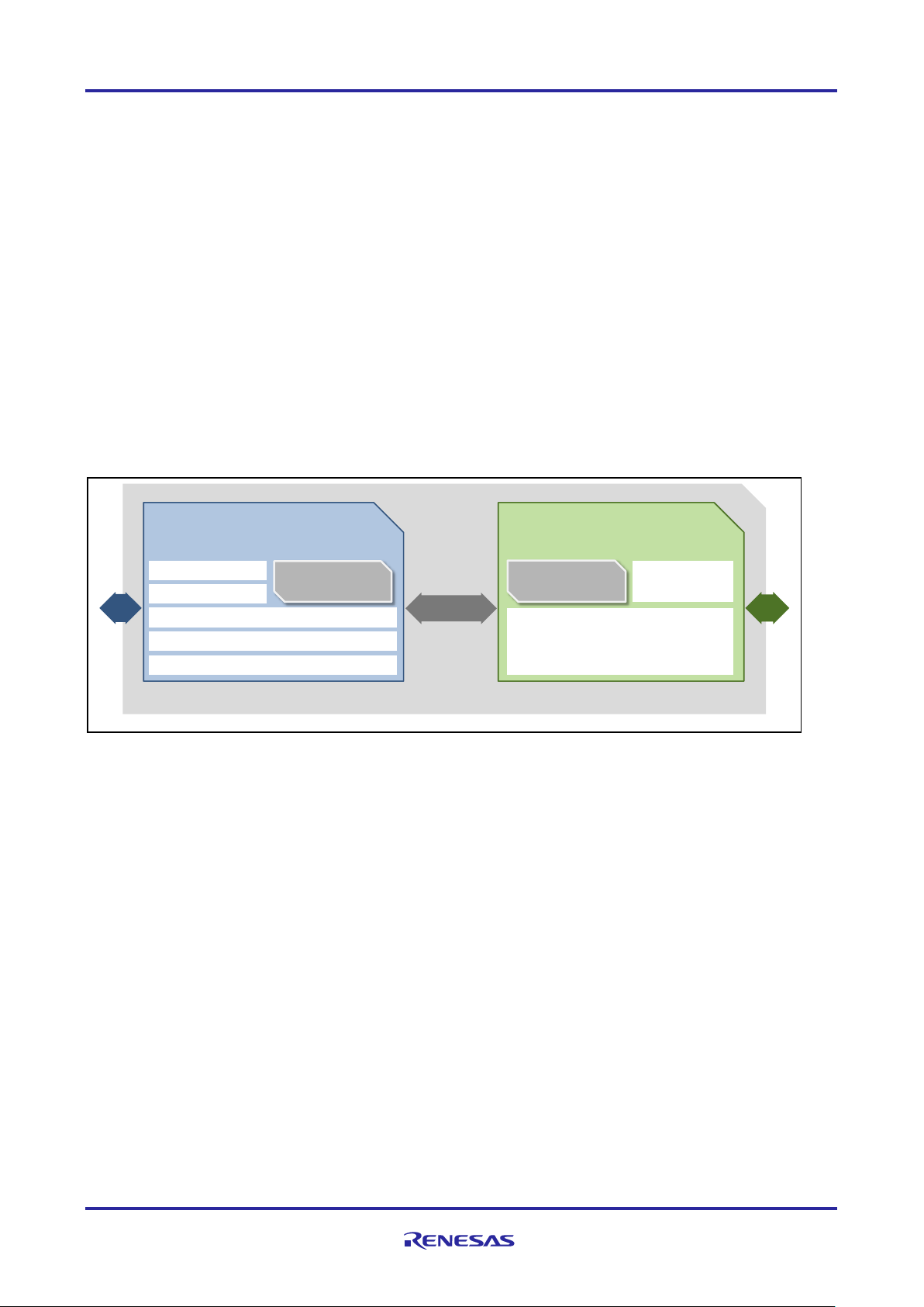
The CONNECT IT! ETHERNET RZ/N1S Solution Kit is based on the RZ/N1S, a 3/5-port, industrial Ethernet
communication SoC in a 324BGA / 196BGA package. RZ/N1D features two independent blocks integrated in
a single package – a communication block based on the proven multi-protocol R-IN Engine, as well as an
application block and a variety of peripherals. In contrast to the RZ/N1D, RZ/N1S includes only a single ARM®
Cortex®-A7 CPU without an external DDR interface, but with 6MB internal SRAM. Please refer to the RZ/N1S
device documentation for further differences. Also, the RZ/N1S Solution Kit contains everything you need for
fast evaluation and rapid prototyping of multiple industrial Ethernet protocols.
The RZ/N1S Solution Kit contains
• RZ/N1S CPU Development Board
• IAR I-jet Lite debugger (incl. 20pin flat ribbon and USB-micro/A cable)
• USB Cable Micro / Type-A
• DVD RZ/N1x-DB Solution Kit for all RZ/N1x devices / boards
Additionally, one can order the RZ/N1-EB Expansion Board separately, that provides the user with the
possibility to use an expanded range of functionalities and RZ/N1S interfaces. RZ/N1-EB kit contains:
• RZ/N1-EB Expansion Board
• Power Supply 24V/750mA
• Power Supply Primary Adapters Euro/UK/JPN-US
The expansion board has no stand-alone capability and requires an RZ/N1D or RZ/N1S CPU board.
RZ/N1S
APPLICATION
ThreadX
6MB SRAM
QSPI/NAND
CAN/UART/I2C
SDIO/USB
HD Display Controller
Arm®Cortex®–A7
ETHERNET COMMUNICATION
uItron + HWRTOS
Multi-Protocol
Industrial Ethernet
Arm®Cortex®–M3
5 Port Real-Time
Ethernet Switch
GOAL
C2C
Communication
324BGA (15x15mm, 0.8mm pitch)
196BGA(12x12mm, 0.8mm pitch)
Figure 1-1: RZ/N1S Functional and HW overview
Page 4
RZ/N1S Group CONNECT IT! ETHERNET RZ/N1S-DB
R01QS0021ED0060 Rev. 0.60 Page 4 of 24
Jan.31.2020
2. Hardware Setup
2.1 CPU Demo Board Setup
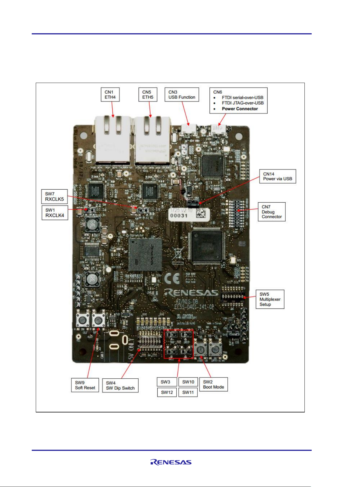
To get started quickly with the board, please identify the connectors on the RZ/N1S-DB CPU Board.
Figure 2-1: Board connectors overview
Page 5
RZ/N1S Group CONNECT IT! ETHERNET RZ/N1S-DB
R01QS0021ED0060 Rev. 0.60 Page 5 of 24
Jan.31.2020
1. Switches and Jumpers
Please take care that the following switches are set.
Table 1: RZ/N1S GPIO Multiplexer DIP-Switch SW5
Number
SW ON (low)
SW OFF (high)
Default
Setting
1
RMII/MII
LCD
OFF
2
CAT/S3
PMOD
ON*
3
MSEBI
Mixed
OFF
4
RMII2 / MDIO 3
QSPI2-Memory
OFF
5
USB 1x Host 1x Device
USB 2 x Host
ON
6
ARM Debug**
FTDI Debug
ON
7
Segger Debugger
I-Jet Debugger
OFF
8
Not used
Not used
OFF
*PHY reset available only in PMOD configuration
**ARM serial debug feature is not supported with the RZ/N1S demo board from the solution kit package
Table 2: RZ/N1S Boot Config DIP-Switch SW4
Switch
SW ON (white bar)
SW OFF
Default
Setting
SW3
JTAG Mode
ARM Coresight Mode
OFF
SW10
Boot from NAND
Boot from QSPI/USB
OFF
SW11
LCD pull up
LCD pull down
ON
SW12
LCD pull up
LCD pull down
ON
SW1
RXCLK4 from PHY
RXCLK4 from GPIO61
ON
SW7
RXCLK5 from PHY
RXCLK5 from GPIO61
ON
Please refer to the schematics
Table 3: Ethernet RX Clock Selection
SW1:
RX_CLK4 Setting
Switch
On Setting (white bar) (default)
Off Setting
SW1
RXCLK4 from Phy
RXCLK4 from GPIO61
SW7:
RX_CLK5 Setting
Page 6
RZ/N1S Group CONNECT IT! ETHERNET RZ/N1S-DB
R01QS0021ED0060 Rev. 0.60 Page 6 of 24
Jan.31.2020
Switch
On Setting (white bar) (default)
Off Setting
SW7
RXCLK5 from Phy
RXCLK5 from GPIO61
Table 4: Jumper Settings RZ/N1S-DB
USB Power
Jumper
On Setting (default)
Off Setting
CN14
Power from USB
Power from expansion board
SRESET from Debugger to RZ/N1D
Jumper
On Setting (default)
Off Setting
CN10
RZ/N1D is connected with the
SRESET from the Debugger
Debugger cannot reset the CPU
MRESETout
Jumper
On Setting
Off Setting (default)
CN9
MRESETOUT is connected to
the Debugger
Debugger cannot detect any
internal CPU reset
USB Host/Device Mode
Jumper
On Setting
Off Setting (default)
CN2
OTG mode ID
Peri Mode ID
Table 5: Push buttons
SW2:
Boot Mode Select
In case SW3 (2) has selected QSPI it is possible to boot from USB instead of the QSPI if SW2 is
pressed down during RESET.
Switch
On Setting
Off Setting
SW2
Boot from USB
Boot from QSPI
Table 6: Reset and NMI Button
SW8
Page 7
RZ/N1S Group CONNECT IT! ETHERNET RZ/N1S-DB
R01QS0021ED0060 Rev. 0.60 Page 7 of 24
Jan.31.2020
Power On Clear
Switch
On Setting
Off Setting
SW8
POR Reset
Release POR Reset
SW9:
Soft Reset
Switch
On Setting
Off Setting
SW4
Soft Reset
Release Soft Reset
SW6:
CM3 NMI
Switch
On Setting
Off Setting
SW6
Generate CM3 NMI
Release CM3 NMI
For more information please refer to the hardware setup notes (RZ_N1S_DB_Board_Setup_Notes) and
schematics (RZ_N1S_DB_Board_Schematic) in respective board documentation folder in Solution Kit.
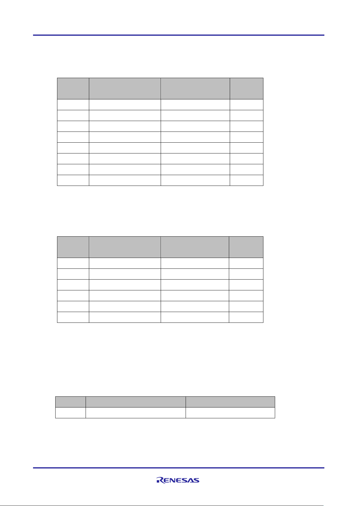
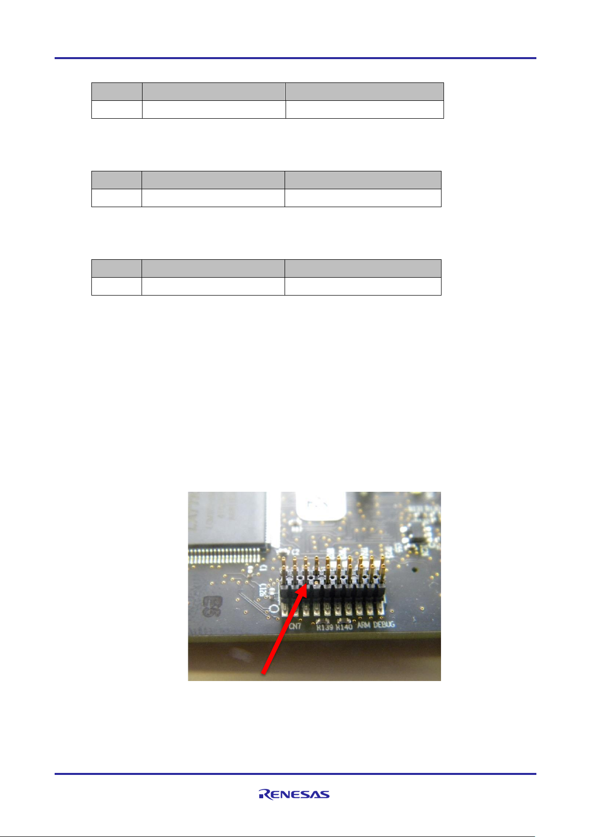
1. JTAG Debug Connector
This connection is required for software development purposes, to be able to run and debug the
software on the target. The IAR Debugger cable has one unused key pin, therefore pin 7 of the CN7
connector should be cut or bent, as shown below. After this step, you can attach your I-jet debugger
to the board via JTAG cable.
Figure 2-2: Connector CN10 with removed pin 7
Page 8
RZ/N1S Group CONNECT IT! ETHERNET RZ/N1S-DB
R01QS0021ED0060 Rev. 0.60 Page 8 of 24
Jan.31.2020
Figure 2-3: I-Jet Debugger connection
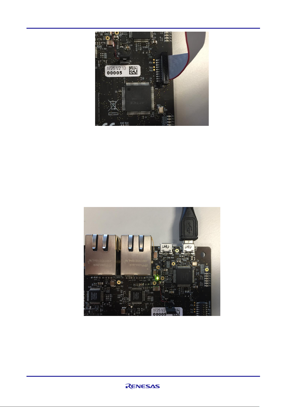
2. Power connector and serial-over-USB
The board is powered via USB connector CN6. Please make sure that the jumper CN14 is ON.
Please connect the board to your PC via USB cable to the connector CN6. The same interface is
used for serial UART communication with the board, so if you have a windows PC, after connecting
the board via USB, you should be able to see a new device registered with 4 new USB Serial COM
ports. You may use any of the terminal emulator on your PC to open a serial port connection to the
board. The board uses the 3rd port for UART output at 115200,8,n,1. On Linux PCs, if you have no
other serial-over-USB devices attached, this is accessed using /dev/ttyUSB2, provided you do not
have any other USB devices attached.
Figure 2-4: Power connector and serial over USB
If the board is not recognized by Windows, please install the FTDI driver that you may find under
…\YCONNECT-IT-RZN_V1.x\Tools\FTDI.
If the required 3.3V are supplied to RZ/N1S, the green LED24 will be lit and stay ON.
Page 9

RZ/N1S Group CONNECT IT! ETHERNET RZ/N1S-DB
R01QS0021ED0060 Rev. 0.60 Page 9 of 24
Jan.31.2020
You can perform a soft-reset of the board by pressing SW9.
3. Ethernet Interface
The Ethernet connection to the PC or a PLC can be prepared using one of the two RJ-45 connectors
CN5 or CN1, as shown in Figure 2-5: Ethernet RJ-45 connectorsFigure 2-5. For running the
EtherCAT sample program you can use any of the two connectors. There are two PHY Micrel chips
connected to these RJ-45 connectors.
Figure 2-5: Ethernet RJ-45 connectors
Page 10

RZ/N1S Group CONNECT IT! ETHERNET RZ/N1S-DB
R01QS0021ED0060 Rev. 0.60 Page 10 of 24
Jan.31.2020
2.2 Expansion Board Setup
If you are using the expansion board together with your RZ/N1S CPU Board, here you may find some setup
notes for it. For more information refer to the board documentation in the Solution Kit. The expansion board
comes with an external power supply to drive the expansion board and the RZ/N1x CPU board plugged onto
the connectors J1 and J2. Please note the position of the power supply selection jumper below and ensure
that the 12…24V position is chosen. This board expands the RZ/N1S CPU boards with 3 Gbit PHY ports, an
SD-Card slot, a USB Host as well as CAN, RS232, RS485, PMODs, LCD display interface with integrated
touch screen, etc.
Figure 2-6: RZ/N1-EB Expansion Board Overview
Page 11

RZ/N1S Group CONNECT IT! ETHERNET RZ/N1S-DB
R01QS0021ED0060 Rev. 0.60 Page 11 of 24
Jan.31.2020
If using the RZ/N1-EB expansion board, please ensure the following jumper and switch settings.
Table 7: Expansion Board switch settings
CN10
CAN Rx
Connect pins 1 and 2 (CAN2)
CN11
CAN Tx
Connect pins 1 and 2 (CAN2)
CN15
PHY2/PHY3 MDC
Connect pins 2 and 3 (MDIO2)
CN16
PHY2/PHY3 MDIO
Connect pins 2 and 3 (MDIO2)
CN17
PHY1 MDC
Connect pins 1 and 2 (MDIO1)
CN18
PHY1 MDIO
Connect pins 1 and 2 (MDIO1)
J18
I2C SDA
Connect pins 1 and 2
J18
I2C SCL
Connect pins 3 and 4
W6
CAN Isolation
NO_ISO
W7
CAN Power
NO_ISO
IMPORTANT INFORMATION: Please take care about using the right 5V power supply when modifiying the
power scheme with CN14 from 12-24V to 5V! A wrong power supply can destroy the Expansion board and the
CPU board powered via the circular power supply connector J4!
Page 12

RZ/N1S Group CONNECT IT! ETHERNET RZ/N1S-DB
R01QS0021ED0060 Rev. 0.60 Page 12 of 24
Jan.31.2020
3. Software Setup
RZ/N1S Solution Kit contains a software package on a DVD that enables the user to evaluate various
functionalities of our industrial automation multi-core chip.
The software for RZ/N1S comes as IAR compilable code and you need IAR Embedded Workbench for ARM
(EWARM) for compiling and running the software on both cores. Since RZ/N1S is a dual-core device, Table 8
gives an overview of development environments for both cores.
Table 8: Development Environment for RZ/N1S
Device
RZ/N1S
CPU
Cortex-A7
Cortex-M3
(R-IN engine)
OS
ThreadX
uITRON
(HWRTOS)
IDE
IAR EWARM
IAR EWARM
Bootloader
U-Boot*
*U-Boot is used as bootloader, it runs on Cortex A7, but it can boot images to be executed on
both cores.
Please follow the below steps to setup the software environment for RZ/N1S.
1. Install IAR EWARM
As the first step in software setup, please install the IAR EWARM -> installation file for IAR EWARM
8.22.1 can be found under YCONNECT-IT-RZN_V1.x\Tools\IAREWARM.
Please note that the current RZ/N1S software from the Solution Kit was tested only with IAR EWARM
v8.22.1. During the installation process, you will be prompted to select your license type. For evaluation
purposes, you can first choose the 30-day license.
2. Locate the RZ/N1S IAR software projects in the Solution Kit
The software is stored in the folder YCONNECT-IT-RZN_V1.x\Software in the Solution Kit. This folder
consists of software packages for all RZ/N1 platforms, not only for RZ/N1S. It is therefore important to
mention which projects are meant for being executed on RZ/N1S and how to differentiate between
projects running on Cortex A7 and on Cortex M3. Table 9 gives an overview about that.
More detailed software documentation can be found under YCONNECT-IT-
RZN_V1.x\Documents\RZN.Software. The IAR projects represent a collection of required source
files to build a Cortex M3 or Cortex A7 executable and run it on the target.
Page 13

RZ/N1S Group CONNECT IT! ETHERNET RZ/N1S-DB
R01QS0021ED0060 Rev. 0.60 Page 13 of 24
Jan.31.2020
Table 9: Overview of IAR Projects for RZ/N1S
IAR Project
Description
CPU
Path to the workspace file in the Sol. Kit
YCONNECT-IT-RZN_V1.x\Software\...
x-ware*
Set of projects
running on the
Cortex A7
including ThreadX,
NetX Duo and
GUIx sample
applications
Cortex A7
\ThreadX\rzn1\iar\x-ware_platform.eww
GOAL
Projects**
Several example
projects showing
the different
functionalities for
the switch
management and
GOAL
Cortex M3
\GOAL\goal\projects\00410_goal\
Protocol
Stack
Projects***
Several Protocol
Stack slave
application
examples, which
are running I/O
communication
between a PLC
and RZ/N1S
Cortex M3
\GOAL\goal\projects\goal_ecat\
\GOAL\goal\projects\goal_eip_lib\
\GOAL\goal\projects\goal_epl_lib\
\GOAL\goal\projects\goal_mbs\
\GOAL\goal\projects\goal_pnio_lib\
* x-ware User Guide:
\YCONNECT-IT-RZN_V1.X\Software\ThreadX\rzn1\docs\X-Ware_Platform_RZ_N1_User_Guide.pdf
** GOAL application notes document:
\YCONNECT-IT-RZN_V1.X\Software\GOAL\doc\r11qs0008ed0131-rzn1-goal-quick-startguide-management.pdf
*** Protocol Stack quick start guides:
\YCONNECT-IT-RZN_V1.X\Software\GOAL\doc\r01an4239ej0090-rzn1-ethercat.pdf
\YCONNECT-IT-RZN_V1.X\Software\GOAL\doc\r11qs0007ed0131-rzn1-goal-quick-startguide-eip.pdf
\YCONNECT-IT-RZN_V1.X\Software\GOAL\doc\r11qs0010ed0131-rzn1-goal-quick-startguide-profinet.pdf
\YCONNECT-IT-RZN_V1.X\Software\GOAL\doc\r01an4412ej0090-rzn1-modbus.pdf
\YCONNECT-IT-RZN_V1.X\Software\GOAL\doc\r11qs0009ed0131-rzn1-goal-quick-startguide-powerlink.pdf
3. Write U-Boot to QSPI flash on the board
As you can see in Table 8, U-Boot is chosen as the secondary bootloader. It runs on the Cortex A7,
initializes some of the required interfaces and peripherals and it can be used to load software images for
both cores, by setting the corresponding parameters in the U-boot user console. Without U-Boot, you
cannot initiate the load of your application via IAR I-Jet Debugger to SRAM for executing on the target.
Figure 3-1 provides an overview of execution stages during programming U-Boot in Flash and later when
U-Boot is configured to read Cortex M3 and Cortex A7 Images from Flash and execute them.
After hardware reset, BootROM will start looking for the U-Boot package in QSPI. Therefore, you need to
write U-Boot in QSPI. This is done via USB DFU (Device Firmware Update). SW5 button pressed together
SW4 signals to BootROM, to switch the boot mode from QSPI to USB DFU. This is required only once, to
load U-Boot to SRAM. In the next step, you will write the U-Boot in flash. Please make sure to connect
CN3 on the board to a USB Host connector on your PC. This provides USB DFU.
Page 14
RZ/N1S Group CONNECT IT! ETHERNET RZ/N1S-DB
R01QS0021ED0060 Rev. 0.60 Page 14 of 24
Jan.31.2020
a. Download the Windows version of dfu-util from https://sourceforge.net/projects/dfu-util/files and
unpack the zip file. No installation is required, where this document tells you to run dfu-util, simply run
the dfu-util-static.exe Windows executable from a Windows command prompt. If you are running Linux
on your PC, install the “dfu-util” package: sudo apt-get install dfu-util.
b. Start the DFU target
Connect your RZ/N1 board to your Windows PC using the USB cable, and reset your board in “Boot
from USB” mode (i.e. using DFU)
c. Register the USB device
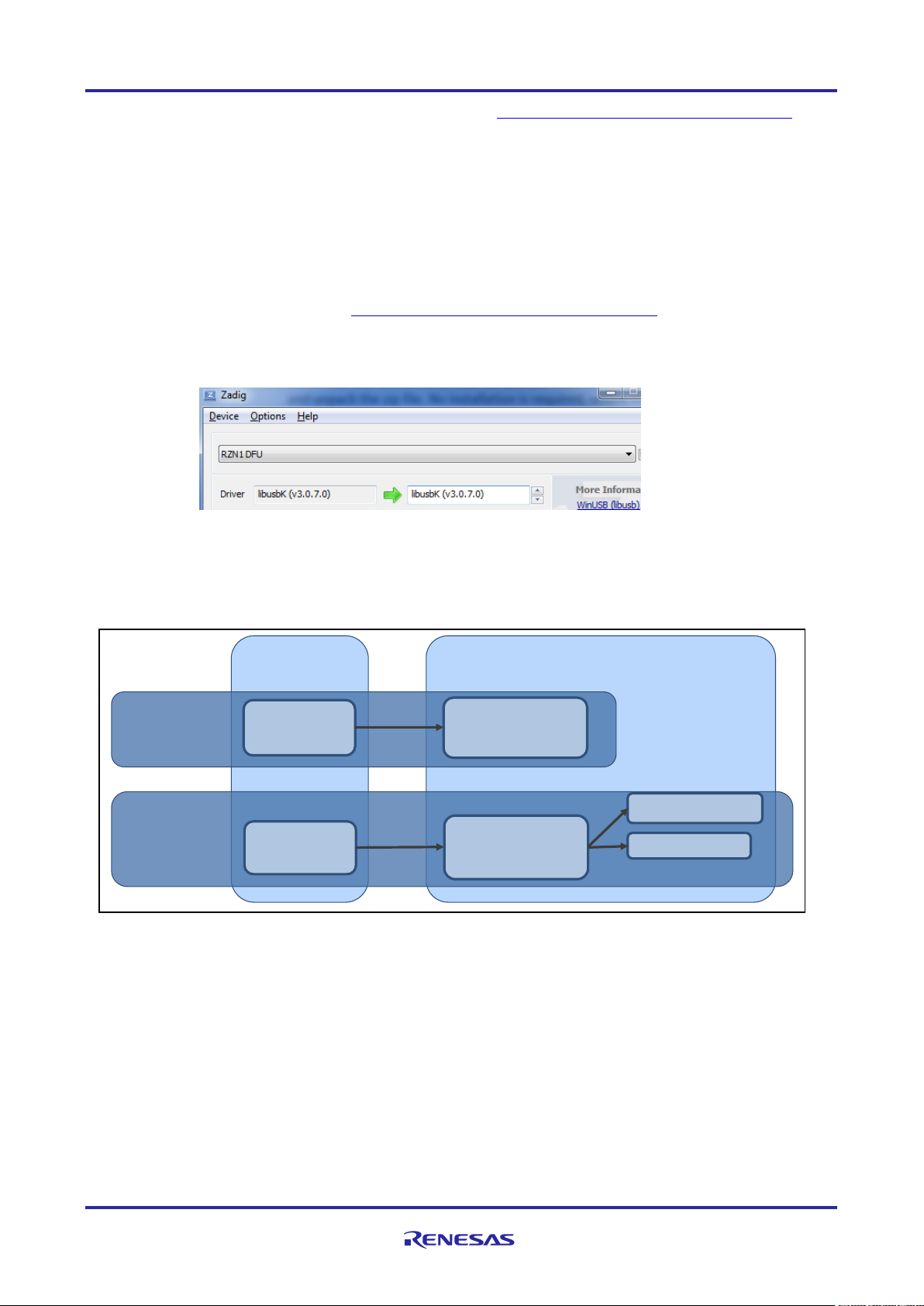
You must register the USB Download Gadget device with the libusbk driver, you only need to do this
once. On your Windows PC:
o Download Zadig from http://zadig.akeo.ie/downloads/zadig-2.3.exe
o Launch Zadig, select "List All Devices" from the Options menu.
o Select "RZN1 DFU" from the pull-down list. Please note that the device might appear as “USB
Download Gadget”
o Select "libusbK" from the Target Driver list (to the right of the green arrow).
o Click the "Install Driver" button, this will take some time.
o Quit Zadig
d. Locate the U-Boot binary for RZ/N1S - YCONNECT-IT-RZN_V1.X\Software\U-Boot-and-Linux\u-
boot\binaries\u-boot-rzn1s324-db.bin.spkg
e. Open a terminal emulator client like TeraTerm or putty, choose the corresponding serial port, where
you board is registered to and set the serial port settings as depicted below. On Linux PCs, if you
have no other serial-over-USB devices attached, board’s serial port is accessed via /dev/ttyUSB2.
Executes in SRAM
Executes in ROM
Programming
Boot from
USB DFU
BootROM
read: USB DFU
write: SRAM
U-Boot
read: USB DFU
write: QSPI
Development
Boot from
SPI Flash
BootROM
read: QSPI
write: SRAM
U-Boot
read: QSPI
write: SRAM
R-IN Engine (CM3)
ThreadX
Figure 3-1: Flash and Boot Sequence
Page 15

RZ/N1S Group CONNECT IT! ETHERNET RZ/N1S-DB
R01QS0021ED0060 Rev. 0.60 Page 15 of 24
Jan.31.2020
f. On the board, hold down switch SW2 (to select DFU
boot mode instead of QSPI) and press switch SW9 (soft reset). The RZ/N1 serial port should output:
** BOOTLOADER STAGE0 for RZN1 **
Boot source: USB
Download U-Boot to SRAM. On your host PC run:
dfu-util.exe -D "u-boot-rzn1s324-db.bin.spkg" in Windows from a Windows
command prompt
sudo dfu-util -D u-boot-rzn1s324-db.bin.spkg in Linux from the terminal
U-Boot should run and the RZ/N1 serial port presents you with a console, like this:
U-Boot 2017.01
Model: RZ/N1S-DB board
DRAM: 4 MiB
MMC: sdhci@0x40100000: 0
SF: Detected mx25l25635f with page size 256 Bytes, erase size 64 KiB,
total 32 MiB, mapped at 10000000
In: serial@0x40060000
Out: serial@0x40060000
Err: serial@0x40060000
Net: dwmac.44000000, dwmac.44002000
Hit any key to stop autoboot: 0
Note: If your board has previously been used and already has U-Boot environment variables
programmed into QSPI, U-Boot may attempt to start running the commands specified by the
bootcmd env variable. Interrupt this by pressing any key.
g. If your board has been programmed with an older version of U-Boot, the dfu_ext_info environment
variable may be incompatible. If so, at the U-Boot console please run:
env default -f dfu_ext_info
saveenv
h. Ensure the U-Boot/SPL region of QSPI Flash is erased, run:
sf probe
sf erase 0 10000
Page 16

RZ/N1S Group CONNECT IT! ETHERNET RZ/N1S-DB
R01QS0021ED0060 Rev. 0.60 Page 16 of 24
Jan.31.2020
i. On the U-Boot console, run:
dfu
j. Write U-Boot to QSPI. On your host PC run:
dfu-util.exe -a "sf_uboot" -D "u-boot-rzn1s324-db.bin.spkg" in Windows
sudo dfu-util -a "sf_uboot" -D u-boot-rzn1s324-db.bin.spkg in Linux
Wait until it completes, the U-Boot console will prompt you to press Ctrl-C when done.
Note: The "sf_uboot" DFU target corresponds to the second region of the QSPI Flash. If there is a
valid SPKG written into the first region ("sf_spl"), the BootROM will load this instead of U-Boot.
Otherwise the BootROM will output messages whilst it looks for the first valid SPKG, like:
STATUS: Valid SPKG header not found (100 QSPI Flash 256-byte blocks read)
k. Press switch SW9 to reset the board, the BootROM will load and run U-Boot showing the following
output on the terminal:
** BOOTLOADER STAGE0 for RZN1 **
Boot source: QSPI
00 BOOTLOADER STAGE0 Success
*** Bootloader stage0 END ***
*** Execute 2nd Stage Bootloader which has been loaded and verified ***
U-Boot 2017.01
Model: RZ/N1S-DB board
DRAM: 4 MiB
MMC: sdhci@0x40100000: 0
SF: Detected mx25l25635f with page size 256 Bytes, erase size 64 KiB,
total 32 MiB, mapped at 10000000
In: serial@0x40060000
Out: serial@0x40060000
Err: serial@0x40060000
Net: dwmac.44000000, dwmac.44002000
Hit any key to stop autoboot: 0
l. Setup U-Boot environment variables
This sets up the U-Boot environment variables for your board. From U-Boot, set the MAC addresses
corresponding to the MAC address sticker on the board, for example:
setenv -f ethaddr 74:90:50:02:00:FD
setenv -f eth1addr 74:90:50:02:00:FE
Save the environment variables:
saveenv
We can now proceed with running the sample applications on the board. For more information on U-Boot
BSP for RZ/N1 please refer to YCONNECT-IT-RZN_V1.X\Software\U-Boot-and-Linux\Documentation\RZN1U-Boot-User-Manual.pdf.
Page 17
RZ/N1S Group CONNECT IT! ETHERNET RZ/N1S-DB
R01QS0021ED0060 Rev. 0.60 Page 17 of 24
Jan.31.2020
3.1 Running a sample application on the RZ/N1S Board
It is straightforward to run an application on the RZ/N1S. Provided you followed the steps in the hardware
setup chapter and in the previous chapter to write U-boot in QSPI, you need to follow the steps below to load
Cortex M3 or/and Cortex A7 image in SRAM and execute it from there. Additionally, you can write the images
in flash and load them to SRAM after reset, by setting the corresponding U-Boot parameters, as described in
chapter 3.2.
3.1.1 Run and debug Cortex M3 software from RAM with IAR Debugger
1. Power the board and open a serial terminal to U-Boot as explained in the previous chapters
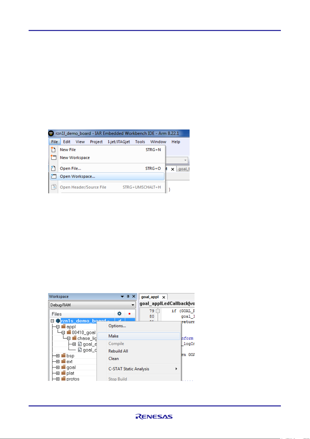
2. Open the IAR EWARM 8.22.1 that you previously installed
3. Click on File -> Open Workspace as depicted below
4. Select the workspace file
YCONNECT-ITRZN_V1.x\Software\GOAL\goal\projects\00410_goal\chase_lights\iar\7_70\rzn1s_demo_board\rzn
1s_demo_board.eww
There are four variants of project settings for each board configuration:
…\7_70\rzn1d_demo_board\rzn1d_demo_board.eww – RZ/N1D CPU Board
…\7_70\rzn1d_demo_board_eb\rzn1d_demo_board_eb.eww – RZ/N1D CPU Board + Expansion
…\7_70\rzn1s_demo_board\rzn1s_demo_board.eww – RZ/N1S CPU Board and
…\7_70\rzn1l_demo_board\rzn1l_demo_board.eww – RZ/N1L CPU Board
5. Select rzn1s_demo_board as shown below, right-click on the project name and click on “Make”.
6. After the project compiled with no errors nor warnings, make sure your board is powered on and that
the IAR I-Jet Debugger is connected to the JTAG connector.
Page 18

RZ/N1S Group CONNECT IT! ETHERNET RZ/N1S-DB
R01QS0021ED0060 Rev. 0.60 Page 18 of 24
Jan.31.2020
7. Click on the “Download and Debug” button in the program control panel in IAR EWARM, as shown
below.
8. In the Debug Log window there should be no errors nor warnings and the program should be stopped
at the beginning of the main() now.
9. At this stage you can click F5 on your keyboard or “Go” button in the IAR program flow panel.
The program should be running now on your board, the LEDs are toggling from one direction to another and
you should see some info output on your serial console as shown below.
Model: RZ/N1S Demo Board
DRAM: 4 MiB
MMC: sdhci@0x40100000: 0
SF: Detected mx25l25635f with page size 256 Bytes, erase size 64 KiB, total 32 MiB, mapped at
10000000
In: serial@0x40060000
Out: serial@0x40060000
Err: serial@0x40060000
Net: , dwmac.44002000
Hit any key to stop autoboot: 0
=> [CC_I|goal_lmLogLegacy:1152] [I|goal_cmInit:209] Calculated config size of 656 in 3 modules
[CC_I|goal_lmLogLegacy:1152] [I|goal_queuePoolBufsReq:776] ID(35) requests buffers[1556]
[CC_I|goal_lmLogLegacy:1152] [I|goal_queuePoolBufsReq:777] fixed/temp = 1, 0
[CC_I|goal_lmLogLegacy:1152] [I|goal_queuePoolBufsReq:776] ID(35) requests buffers[1556]
Page 19

RZ/N1S Group CONNECT IT! ETHERNET RZ/N1S-DB
R01QS0021ED0060 Rev. 0.60 Page 19 of 24
Jan.31.2020
[CC_I|goal_lmLogLegacy:1152] [I|goal_queuePoolBufsReq:777] fixed/temp = 2, 0
[CC_I|goal_lmLogLegacy:1152] [I|goal_queuePoolBufsReq:776] ID(35) requests buffers[1556]
[CC_I|goal_lmLogLegacy:1152] [I|goal_queuePoolBufsReq:777] fixed/temp = 1, 0
[CC_I|goal_lmLogLegacy:1152] [I|goal_taskCreate:74] creating task: Timer
[CC_I|goal_lmLogLegacy:1152] [I|goal_init:190] GOAL initialized
[CC_I|goal_lmLogLegacy:1152] [I|appl_setup:85] Chase Lights application started.
[CC_I|goal_lmLogLegacy:1152] [I|goal_memInitDone:128] fixed memory usage: 16020/196608 bytes
[CC_I|goal_lmLogLegacy:1152] [I|goal_memInitDone:129] fixed memory usage: (9%)
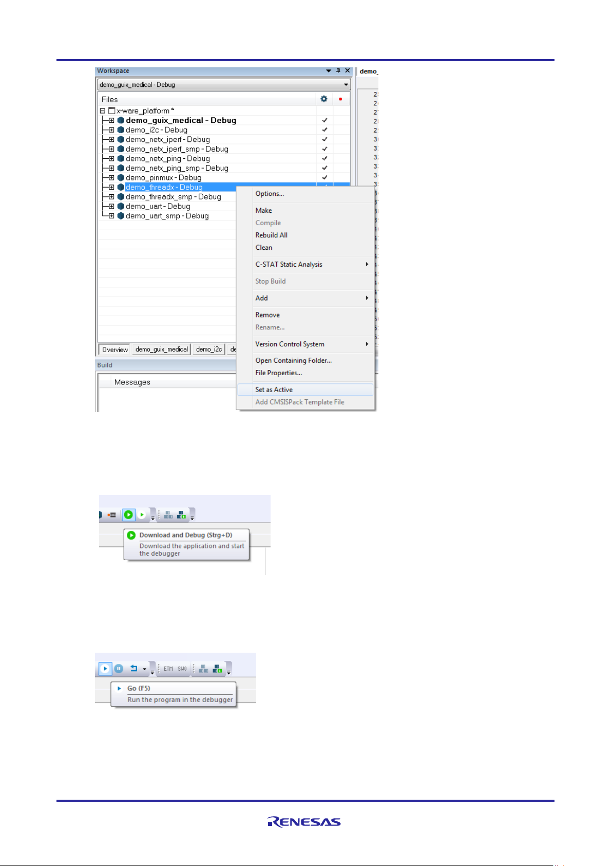
3.1.2 Run and debug Cortex A7 software from RAM with IAR Debugger
The steps are almost the same as the ones described in chapter 3.1.1. Reset the board by pressing SW9.
Follow the steps 1-4 from the previous chapter with the difference that you should open a Cortex A7 workspace
file in IAR EWARM (step 4):
YCONNECT-IT-RZN_V1.X\Software\ThreadX\rzn1\iar\x-ware_platform.eww
Please note that the projects, having their name ending with “_smp” are meant for the execution on the
RZ/N1D. SMP stands for Synchronous Multiprocessing and it matches the architecture of the dual-core Cortex
A7 of RZ/N1D. Nevertheless, you can also run the non-smp projects on RZ/N1D, however smp projects will
not run on the RZ/N1S, since RZ/N1S contains a single-core Cortex A7.
5. After opening the workspace, choose one of the projects in the workspace as shown below. Choose
demo_threadx project as an example.
Page 20
RZ/N1S Group CONNECT IT! ETHERNET RZ/N1S-DB
R01QS0021ED0060 Rev. 0.60 Page 20 of 24
Jan.31.2020
6. Compile the project by clicking “Make”
7. After the project compiled with no errors nor warnings, make sure your board is powered on and that
the IAR I-Jet Debugger is connected to the JTAG connector.
8. Click on the “Download and Debug” button in the program control panel in IAR EWARM, as shown
below.
9. In the Debug Log window there should be no errors nor warnings and the program should be stopped
at the beginning of the main() now.
10. At this stage you can click F5 on your keyboard or “Go” button in the IAR program flow panel.
The program should be running now on your board and you should see some info output on your serial console
as shown below.
Page 21

RZ/N1S Group CONNECT IT! ETHERNET RZ/N1S-DB
R01QS0021ED0060 Rev. 0.60 Page 21 of 24
Jan.31.2020
At the point of releasing this solution kit version, the IAR Embedded Workbench was not configured for multicore debugging (Cortex A7 and Cortex M3 simultaneously).
3.2 Boot a sample application from QSPI flash
To store your binary in QSPI Flash and be able to execute it from there after every new reset, you need to
write the images in flash and set the corresponding U-Boot parameters. Please follow the steps below to do
that.
1. Open an rzn1s_demo_board project for Cortex M3 in IAR, for example:
YCONNECT-ITRZN_V1.x\Software\GOAL\goal\projects\00410_goal\led_demo\iar\7_70\rzn1s_demo_board\rzn1s_
demo_board.eww
2. Right-click on the rzn1s_demo_board and click on “Options”. Click on “Output Converter” in the left
tab of the options window and tick the box “Generate additional output” and select raw binary output
format.
3. Compile the project. Your raw binary is in the exe folder of the project directory, for example
goal\projects\00410_goal\chase_lights\iar\7_70\rzn1s_demo_board\Debug-RAM\Exe
4. Connect CN3 on the board to a USB Host connector on your PC. This provides USB DFU. Reset the
board (SW9) and open the serial terminal to the U-boot console. In the U-boot console type: dfu
Model: RZ/N1S Demo Board
DRAM: 4 MiB
Page 22

RZ/N1S Group CONNECT IT! ETHERNET RZ/N1S-DB
R01QS0021ED0060 Rev. 0.60 Page 22 of 24
Jan.31.2020
MMC: sdhci@0x40100000: 0
SF: Detected mx25l25635f with page size 256 Bytes, erase size 64 KiB,
total 32 MiB, mapped at 10000000
In: serial@0x40060000
Out: serial@0x40060000
Err: serial@0x40060000
Net: , dwmac.44002000
=> dfu
5. Open the command window in Windows or terminal in Linux and type the command to write the raw
binary in flash:
>dfu-util.exe -a "sf_cm3" -D "rzn1s_demo_board.bin" in Windows
sudo dfu-util -a "sf_cm3" -D "rzn1s_demo_board.bin" in Linux
dfu-util 0.9
Copyright 2005-2009 Weston Schmidt, Harald Welte and OpenMoko Inc.
Copyright 2010-2016 Tormod Volden and Stefan Schmidt
This program is Free Software and has ABSOLUTELY NO WARRANTY
Please report bugs to http://sourceforge.net/p/dfu-util/tickets/
Invalid DFU suffix signature
A valid DFU suffix will be required in a future dfu-util release!!!
Opening DFU capable USB device...
ID 045b:0239
Run-time device DFU version 0110
Claiming USB DFU Interface...
Setting Alternate Setting #5 ...
Determining device status: state = dfuIDLE, status = 0
dfuIDLE, continuing
DFU mode device DFU version 0110
Device returned transfer size 4096
Copying data from PC to DFU device
Download [=========================] 100% 40414 bytes
Download done.
state(7) = dfuMANIFEST, status(0) = No error condition is present
state(2) = dfuIDLE, status(0) = No error condition is present
Done!
6. Now your binary is stored in flash and you need to set the U-boot environment variables to boot it
after reset. Please type the following commands in the U-boot console:
Page 23

RZ/N1S Group CONNECT IT! ETHERNET RZ/N1S-DB
R01QS0021ED0060 Rev. 0.60 Page 23 of 24
Jan.31.2020
=> setenv bootcmd "sf probe && sf read 0x4000000 d0000 80000 &&
rzn1_start_cm3"
=> saveenv
After the next reset (SW9), the Cortex M3 image is booted and executed automatically by U-Boot.
If you wish to write Cortex A7 binary in QSPI flash, you need to follow the previous steps 1-4, with the difference
that you need to select the corresponding Cortex A7 project in step 1, instead of Cortex M3 one, for example
demo_threadx project from the workspace YCONNECT-IT-RZN_V1.X\Software\ThreadX\rzn1\iar\x-
ware_platform.eww. The binary file you may find under
YCONNECT-IT-RZN_V1.X\Software\ThreadX\rzn1\iar\demo_threadx\Debug\Exe\demo_threadx.bin
5. Open the command window in Windows or terminal in Linux and type the command to write the Cortex
A7 raw binary in flash:
>dfu-util.exe -a "sf_kernel" -D "demo_threadx.bin" in Windows
sudo dfu-util -a "sf_kernel" -D "demo_threadx.bin" in Linux
6. Now your Cortex A7 binary is stored as well in flash and you need to set the U-boot environment
variables to boot it after reset. Please type the following commands in the U-boot console:
=> setenv bootcmd "dcache off&&sf probe&&sf read 0x80008000 1d0000
600000&&go 0x80008000"
=> saveenv
After the next reset (SW9), the Cortex A7 image is booted and executed automatically by U-Boot.
7. Since now you have both binaries (images) stored in flash, you could theoretically boot and execute
both from U-Boot. To do that, please type the following commands in the U-boot console:
=> setenv bootcmd "sf probe && sf read 0x4000000 d0000 80000 &&
rzn1_start_cm3&&sleep 4&&dcache off&&sf read 0x80008000 1d0000 600000&&go
0x80008000"
=> saveenv
Reset the board – SW9. Now you have both binaries running simultaneously.
Page 24

RZ/N1S Group CONNECT IT! ETHERNET RZ/N1S-DB
R01QS0021ED0060 Rev. 0.60 Page 24 of 24
Jan.31.2020
Revision History
Rev.
Date
Description
Page
Summary
0.1
22.Feb.2018
-
Draft – first revision
0.2
23.Mar.2018
-
Added eth rx clk and push button settings table and dfu-util
driver information
0.3
01.Aug.2018
-
Updates to match to the latest GOAL for solution kit v1.3.1
release
0.4
11.Sep.2018
-
Inserted important notes regarding the flexible power supply
structure on the RZ/N1 Expansion Board
0.5
24.Sep.2019
-
Modified licensing description
0.6
31.Jan.2020
-
Changed format
Page 25

General Precautions in the Handling of Microprocessing Unit and Microcontroller
Unit Products
The following usage notes are applicable to all Microprocessing unit and Microcontroller unit products from Renesas. For detailed usage notes on the
products covered by this document, refer to the relevant sections of the document as well as any technical updates that have been issued for the products.
1. Precaution against Electrostatic Discharge (ESD)
A strong electrical field, when exposed to a CMOS device, can cause destruction of the gate oxide and ultimately degrade the device operation. Steps
must be taken to stop the generation of static electricity as much as possible, and quickly dissipate it when it occurs. Environmental control must be
adequate. When it is dry, a humidifier should be used. This is recommended to avoid using insulators that can easily build up static electricity.
Semiconductor devices must be stored and transported in an anti-static container, static shielding bag or conductive material. All test and
measurement tools including work benches and floors must be grounded. The operator must also be grounded using a wrist strap. Semiconductor
devices must not be touched with bare hands. Similar precautions must be taken for printed circuit boards with mounted semiconductor devices.
2. Processing at power-on
The state of the product is undefined at the time when power is supplied. The states of internal circuits in the LSI are indeterminate and the states of
register settings and pins are undefined at the time when power is supplied. In a finished product where the reset signal is applied to the external reset
pin, the states of pins are not guaranteed from the time when power is supplied until the reset process is completed. In a similar way, the states of pins
in a product that is reset by an on-chip power-on reset function are not guaranteed from the time when power is supplied until the power reaches the
level at which resetting is specified.
3. Input of signal during power-off state
Do not input signals or an I/O pull-up power supply while the device is powered off. The current injection that results from input of such a signal or I/O
pull-up power supply may cause malfunction and the abnormal current that passes in the device at this time may cause degradation of internal
elements. Follow the guideline for input signal during power-off state as described in your product documentation.
4. Handling of unused pins
Handle unused pins in accordance with the directions given under handling of unused pins in the manual. The input pins of CMOS products are
generally in the high-impedance state. In operation with an unused pin in the open-circuit state, extra electromagnetic noise is induced in the vicinity of
the LSI, an associated shoot-through current flows internally, and malfunctions occur due to the false recognition of the pin state as an input signal
become possible.
5. Clock signals
After applying a reset, only release the reset line after the operating clock signal becomes stable. When switching the clock signal during program
execution, wait until the target clock signal is stabilized. When the clock signal is generated with an external resonator or from an external oscillator
during a reset, ensure that the reset line is only released after full stabilization of the clock signal. Additionally, when switching to a clock signal
produced with an external resonator or by an external oscillator while program execution is in progress, wait until the target clock signal is stable.
6. Voltage application waveform at input pin
Waveform distortion due to input noise or a reflected wave may cause malfunction. If the input of the CMOS device stays in the area between VIL
(Max.) and VIH (Min.) due to noise, for example, the device may malfunction. Take care to prevent chattering noise from entering the device when the
input level is fixed, and also in the transition period when the input level passes through the area between VIL (Max.) and VIH (Min.).
7. Prohibition of access to reserved addresses
Access to reserved addresses is prohibited. The reserved addresses are provided for possible future expansion of functions. Do not access these
addresses as the correct operation of the LSI is not guaranteed.
8. Differences between products
Before changing from one product to another, for example to a product with a different part number, confirm that the change will not lead to problems.
The characteristics of a microprocessing unit or microcontroller unit products in the same group but having a different part number might differ in terms
of internal memory capacity, layout pattern, and other factors, which can affect the ranges of electrical characteristics, such as characteristic values,
operating margins, immunity to noise, and amount of radiated noise. When changing to a product with a different part number, implement a systemevaluation test for the given product.
Page 26

© 2019 Renesas Electronics Corporation. All rights reserved.
Notice
1. Descriptions of circuits, software and other related information in this document are provided only to illustrate the operation of semiconductor products
and application examples. You are fully responsible for the incorporation or any other use of the circuits, software, and information in the design of your
product or system. Renesas Electronics disclaims any and all liability for any losses and damages incurred by you or third parties arising from the use
of these circuits, software, or information.
2. Renesas Electronics hereby expressly disclaims any warranties against and liability for infringement or any other claims involving patents, copyrights,
or other intellectual property rights of third parties, by or arising from the use of Renesas Electronics products or technical information described in this
document, including but not limited to, the product data, drawings, charts, programs, algorithms, and application examples.
3. No license, express, implied or otherwise, is granted hereby under any patents, copyrights or other intellectual property rights of Renesas Electronics
or others.
4. You shall not alter, modify, copy, or reverse engineer any Renesas Electronics product, whether in whole or in part. Renesas Electronics disclaims any
and all liability for any losses or damages incurred by you or third parties arising from such alteration, modification, copying or reverse engineering.
5. Renesas Electronics products are classified according to the following two quality grades: “Standard” and “High Quality”. The intended applications for
each Renesas Electronics product depends on the product’s quality grade, as indicated below.
"Standard": Computers; office equipment; communications equipment; test and measurement equipment; audio and visual equipment; home
electronic appliances; machine tools; personal electronic equipment; industrial robots; etc.
"High Quality": Transportation equipment (automobiles, trains, ships, etc.); traffic control (traffic lights); large-scale communication equipment; key
financial terminal systems; safety control equipment; etc.
Unless expressly designated as a high reliability product or a product for harsh environments in a Renesas Electronics data sheet or other Renesas
Electronics document, Renesas Electronics products are not intended or authorized for use in products or systems that may pose a direct threat to
human life or bodily injury (artificial life support devices or systems; surgical implantations; etc.), or may cause serious property damage (space
system; undersea repeaters; nuclear power control systems; aircraft control systems; key plant systems; military equipment; etc.). Renesas Electronics
disclaims any and all liability for any damages or losses incurred by you or any third parties arising from the use of any Renesas Electronics product
that is inconsistent with any Renesas Electronics data sheet, user’s manual or other Renesas Electronics document.
6. When using Renesas Electronics products, refer to the latest product information (data sheets, user’s manuals, application notes, “General Notes for
Handling and Using Semiconductor Devices” in the reliability handbook, etc.), and ensure that usage conditions are within the ranges specified by
Renesas Electronics with respect to maximum ratings, operating power supply voltage range, heat dissipation characteristics, installation, etc. Renesas
Electronics disclaims any and all liability for any malfunctions, failure or accident arising out of the use of Renesas Electronics products outside of such
specified ranges.
7. Although Renesas Electronics endeavors to improve the quality and reliability of Renesas Electronics products, semiconductor products have specific
characteristics, such as the occurrence of failure at a certain rate and malfunctions under certain use conditions. Unless designated as a high reliability
product or a product for harsh environments in a Renesas Electronics data sheet or other Renesas Electronics document, Renesas Electronics
products are not subject to radiation resistance design. You are responsible for implementing safety measures to guard against the possibility of bodily
injury, injury or damage caused by fire, and/or danger to the public in the event of a failure or malfunction of Renesas Electronics products, such as
safety design for hardware and software, including but not limited to redundancy, fire control and malfunction prevention, appropriate treatment for
aging degradation or any other appropriate measures. Because the evaluation of microcomputer software alone is very difficult and impractical, you are
responsible for evaluating the safety of the final products or systems manufactured by you.
8. Please contact a Renesas Electronics sales office for details as to environmental matters such as the environmental compatibility of each Renesas
Electronics product. You are responsible for carefully and sufficiently investigating applicable laws and regulations that regulate the inclusion or use of
controlled substances, including without limitation, the EU RoHS Directive, and using Renesas Electronics products in compliance with all these
applicable laws and regulations. Renesas Electronics disclaims any and all liability for damages or losses occurring as a result of your noncompliance
with applicable laws and regulations.
9. Renesas Electronics products and technologies shall not be used for or incorporated into any products or systems whose manufacture, use, or sale is
prohibited under any applicable domestic or foreign laws or regulations. You shall comply with any applicable export control laws and regulations
promulgated and administered by the governments of any countries asserting jurisdiction over the parties or transactions.
10. It is the responsibility of the buyer or distributor of Renesas Electronics products, or any other party who distributes, disposes of, or otherwise sells or
transfers the product to a third party, to notify such third party in advance of the contents and conditions set forth in this document.
11. This document shall not be reprinted, reproduced or duplicated in any form, in whole or in part, without prior written consent of Renesas Electronics.
12. Please contact a Renesas Electronics sales office if you have any questions regarding the information contained in this document or Renesas
Electronics products.
(Note1) “Renesas Electronics” as used in this document means Renesas Electronics Corporation and also includes its directly or indirectly controlled
subsidiaries.
(Note2) “Renesas Electronics product(s)” means any product developed or manufactured by or for Renesas Electronics.
(Rev.4.0-1 November 2017)
Corporate Headquarters
Contact information
TOYOSU FORESIA, 3-2-24 Toyosu,
Koto-ku, Tokyo 135-0061, Japan
www.renesas.com
For further information on a product, technology, the most up-to-date
version of a document, or your nearest sales office, please visit:
www.renesas.com/contact/.
Trademarks
Renesas and the Renesas logo are trademarks of Renesas Electronics
Corporation. All trademarks and registered trademarks are the property
of their respective owners.
 Loading...