

Page 1
Release Note
RZ/A2M Software Package
S
2D Barcode
Wi
S
for each driver and each middleware.
Examples of application software
projects for 2D barcode scanner.
E
projects for Wi
Other Packages
[will be added]
…
Tools
Hardware
RZ/A2M Group
RZ/A2M SDIO Wi-Fi Package (IAR Embedded Workbench for ARM) V1.00 Release Note
Introduction
This package contains Wireless image streaming sample program for RZ/A2M group microcomputers and
SILEX Technology SX-SDMAC module. SX-SDMAC module (SX-SDCAC-2830-SP
package.
The Software Package shows how easy it is to create a professional, user-friendly and platform-independent
user interface for your product. The entire application source code is included in the workspace enabling the
Software Package to be ported to the platform of your choice.
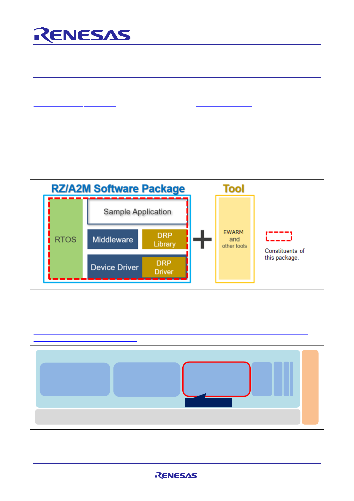
This package is one of RZ/A2M Software Package. RZ/A2M Software Package is a software development kit
for the RZ/A2M that supports various RZ/A2M functions such as DRP (Dynamically Reconfigurable
Processor), camera input, LCD output, and image adj us tment . This package has the structure of the red
frame in the following figure. However, device driver and middleware are only included what is necessary for
the sample application.
) is needed to use this
RZ/A2M Software Package Configuration
Figure below shows the relation of RZ/A2M Software Package and this package. For details, refer following
URL:
https://www.renesas.com/products/software-tools/software-os-middleware-driver/software-package/rza2software-development-kit-free-rtos.html
imple Applications Package
imple software projects include the usage
Package
-Fi Package
xamples of application software
-Fi driver via SDIO..
This package
The relation of RZ/A2M Software Packages and this package
Note that each softwar e proj ec t includes only driver software and middleware used by each application.
R01AN5681EJ0100 Rev.1.00 Page 1 of 8
Jan.29.21
Page 2

RZ/A2M Group RZ/A2M SDIO Wi-Fi Package (IAR Embedded Workbench for ARM) V1.00 Release Note
Following sample applications are bundled in this package.
SX-SDMAC Wi-Fi sample program
This sample program transmits captured images to PC using the SDIO driver and SILEX Technology SX-
SDMAC driver. This sample uses FreeRTOS.
SX-SDMAC Wi-Fi Evaluation sample program
This sample program enables evaluation of Wi-Fi module using command interface. This sample uses
FreeRTOS.
SDIO driver used in this sample does not support Ultra-High-Speed mode. RZ/A2M group RZ/A2M SDIO WiFi Package(NDA) contains driver and sample project that supports the mode. To get this package, please
contact Renesas sales
.
Target Device / Target Board
Target Device: RZ/A2M
Target Board Kit: RZ/A2M Evaluati on Board Kit (RTK7921053S00000BE)
Target Module: SILEX Technology SX-SDCAC-2830-SP
R01AN5681EJ0100 Rev.1.00 Page 2 of 8
Jan.29.21
Page 3

RZ/A2M Group RZ/A2M SDIO Wi-Fi Package (IAR Embedded Workbench for ARM) V1.00 Release Note
Contents
1. Package Contents ................................................................................................................... 4
1.1 Software .................................................................................................................................................. 4
1.2 Documents .............................................................................................................................................. 4
2. Folder Structure ....................................................................................................................... 4
3. How to use the projects bundled in this package ..................................................................... 5
4. Reference Application Notes ................................................................................................... 5
5. Restrictions .............................................................................................................................. 5
6. Precautions ............................................................................................................................. 6
7. Used open source software and licenses ................................................................................. 7
Revision History .............................................................................................................................. 8
R01AN5681EJ0100 Rev.1.00 Page 3 of 8
Jan.29.21
Page 4

RZ/A2M Group RZ/A2M SDIO Wi-Fi Package (IAR Embedded Workbench for ARM) V1.00 Release Note
No
Name
File name
1
RZ/A2M Group SX-SDMAC Wi-Fi sample
Application
2
RZ/A2M Group SX-SDMAC Wi-Fi Evaluation
Sample Application
+---r01qs0034jj0103-rza2m-quick-guide-iar.pdf : RZ/A2M Group RZ/A2M Software Package Quick Start Guide (Japanese)
No
Title
Document Number
1
RZ/A2M Group RZ/A2M SDIO Wi-Fi Package (IAR Embedded
R01AN5681
(This document)
2
RZ/A2M Group RZ/A2M Software Package Quick Start Guide
R01QS0027
1. Package Contents
1.1 Software
This package contains the following software.
Table 1-1 Software of this package
rza2m_wifi_sx_sdmac_sample_freertos_iar.zip
rza2m_wifi_sx_sdmac_eval_sample_nda_freertos_iar.zip
1.2 Documents
This package contains the following documents.
Table 1-2 Documents of this package
Workbench for ARM) V1.00 Release Note
Also, the project indicated in Table 1-1 includes the sample program’s application note.
2. Folder Structure
Folder structure of this package and outline of contents are shown as follow.
TOP : top folder
|
+---rza2m_wifi_sx_sdmac_sample_freertos_iar.zip : RZ/A2M Group SX-SDMAC Wi-Fi sample Application
+---rza2m_wifi_sx_sdmac_eval_sample_freertos_iar.zip : RZ/A2M Group SX-SDMAC Wi-Fi Evaluation sample Application
+---r01an5681ej0100-rza2m-wifi-swpkg-iar.pdf : RZ/A2M Group RZ/A2M SDIO Wi-Fi Package (IAR Embedded Workbench for ARM)
+---r01an5681jj0100-rza2m-wifi-swpkg-iar.pdf : RZ/A2M Group RZ/A2M SDIO Wi-Fi Package (IAR Embedded Workbench for ARM)
+---r01qs0034ej0103-rza2m-quick-guide-iar.pdf : RZ/A2M Group RZ/A2M Software Package Quick Start Guide (English)
Figure 2.1 Folder Structure
V1.00 Release Note (this document)
V1.00 Release Note (Japanese)
R01AN5681EJ0100 Rev.1.00 Page 4 of 8
Jan.29.21
Page 5

RZ/A2M Group RZ/A2M SDIO Wi-Fi Package (IAR Embedded Workbench for ARM) V1.00 Release Note
No.
Type
Description
1
DRP Driver *
The following API Functions are not supported.
"R_DK2_ERR_INTERNAL".
2
DRP Driver *
The function that loads the configuration data in background is not supported.
error and return "R_DK2_ERR_INTERNAL".
3
DRP Driver *
R_DK2_Load Function notifies the return value "R_DK2_ERR_DEVICE", when
function is not supported.
4
DRP Driver *
Processing Completion Callback Function notifies the argument "result" is
this package this function is not supported.
5
DRP Driver *
Processing Completion Callback Function notifies the argument "result" is
package this function is not supported.
6
SDIO Driver
It is required that remove and insert Wi-Fi module after downloading before running.
7
SX-SDMAC
driver
DHCP setting is fixed to use. ipconfigUSE_DHCP and configIP_ADDR settings are
ignored.
3. How to use the projects bundled in this package
Regarding how to use, refer to the documents in each folder in this package.
4. Reference Application Notes
Following is the list of application notes related to this software package.
RZ/A2M Group RZ/A2M Software Core Package (R01AN5528).
Drivers and middleware for RZ/A2M that can be added to the project bundled in this package.
5. Restrictions
The Restrictions of this package are shown as follow.
Table 6-1 Restrictions
- R_DK2_Uninitialize
- R_DK2_Inactivate
If these functions are called, these functions occur an error and return
This function validates when argument "pload" of R_DK2_Load Function is set to
anything other than NULL. In the version in this package this function occurs an
detects a transfer error of the configuration data. In the version in this pack age th is
"R_DK2_ERR_DEVICE", when detects a transfer error in DRP. In the version in
"R_DK2_ERR_STOPPED", when detects a transfer stopped by calling
R_DK2_Unload Function of R_DK2_Inactivate Function. In the version in this
* Please refer to "RZ/A2M Group DRP Driver User's Manual(R01US0355)" for details of DRP Driver's
function.
R01AN5681EJ0100 Rev.1.00 Page 5 of 8
Jan.29.21
Page 6

RZ/A2M Group RZ/A2M SDIO Wi-Fi Package (IAR Embedded Workbench for ARM) V1.00 Release Note
No.
Type
Description
1
Environment
If it is happened a build error while building the project of this package as it is, the
Install IAR Embedded Wor kbenc h® for ARM v8.40.1 or later again.
2
Environment
To avoid build error, expand the project to the folder with short full path.
3
Environment
To avoid build error, expand the project to the folder without multi-byte character.
4
File System
src\fatfs\documents.zip includes *.c files. If you unzipped the zip file, exclude the
documents\res from your build.
5
All
Since V1.01, the folder structure of the project using FreeRTOS has been changed
Therefore, they are incompatible with the project between V1.01 later and V1.00.
6. Precautions
The Precautions of this package are shown as follow.
Table 7-1 Precautions
setting of environme nt may be incorrect.
Check following items:
• Follow section 3 of “RZ/A2M Software Package Quick Start Guide”(R01QS0027)
•
to follow Amazon FreeRTOS.
R01AN5681EJ0100 Rev.1.00 Page 6 of 8
Jan.29.21
Page 7

RZ/A2M Group RZ/A2M SDIO Wi-Fi Package (IAR Embedded Workbench for ARM) V1.00 Release Note
7. Used open source software and licenses
Open source software used in this package and license of them are shown as following:
• SX-SDMAC driver is used under the license of SILEX technology described before downloading this
package.
• newlib is used under the license described in following site:
https://www.sourceware.org/newlib/COPYING.NEWLIB
• FreeRTOSTM is a trademark of Amazon Web Services, Inc.
• FreeRTOS is used under MIT license described in following site:
https://www.freertos.org/a00114.html
https://github.com/aws/amazon-freertos/blob/master/LICENSE
https://aws.amazon.com/jp/freertos/faqs/
• FatFs is used under the license described in following site:
http://elm-chan.org/fsw/ff/doc/appnote.html#license
SD Host/Ancillary Product License Agreement (SD HALA) is required to develop SD host-related products.
Refer https://www.sdcard.org/developers/licensing/
for detail:
R01AN5681EJ0100 Rev.1.00 Page 7 of 8
Jan.29.21
Page 8

RZ/A2M Group RZ/A2M SDIO Wi-Fi Package (IAR Embedded Workbench for ARM) V1.00 Release Note
Rev.
Date
Description
Page
Summary
1.00
Jan.29.21
-
First Edition issued
Revision History
R01AN5681EJ0100 Rev.1.00 Page 8 of 8
Jan.29.21
Page 9

General Precautions in the Handling of Microprocessing Unit and Microcontrolle r Unit Products
The following usage notes are applicable to all Microprocessing unit and Microcontroller unit products from Renesas. For detailed usa ge no tes on th e
products covered by this document, refer to the relevant sections of the document as well as any technical updates that have been issued for the products.
1. Precaution against Electrostatic Discharge (ESD)
A strong electrical field, when exposed to a CMOS device, can cause destruction of the gate oxide and ultimately degrade the device operation. Steps
must be taken to stop the generation of static electricity as much as possible, and quickly dissipate it when it occurs. Environmental control must be
adequate. When it is dry, a humidifier should be used. This is recommended to avoid using insulators that can easily build up static electricity.
Semiconductor devices must be stored and transported in an anti-static container, static shielding bag or conductive material. All test and
measurement tools including work benches and floors must be grounded. The operator must also be grounded using a wrist strap. Semiconductor
devices must not be touched with bare hands. Similar precautions must be taken for printed circuit boards with mounted semiconductor devices.
2. Processing at power-on
The state of the product is undefined at the time when power is supplied. The states of internal circuits in the LSI are indeterminate and the states of
register settings and pins are undefined at the time when power is supplied. In a finished product where the reset signal is applied to the ex t er nal reset
pin, the states of pins are not guaranteed from the time when power is supplied until the reset process is completed. In a similar way, the states of pins
in a product that is reset by an on-chip power-on reset function are not guaranteed from the time when power is supplied until the power reaches the
level at which resetting is specified.
3. Input of signal during power-off state
Do not input signals or an I/O pull-up power supply while the device is powered off. The current injection that results from input of such a signal or I/O
pull-up power supply may cause malfunction and the abnormal current that passes in the device at this time may cause degradation of internal
elements. Follow the guideline for input signal during power-off state as described in your product documentation.
4. Handling of unused pins
Handle unused pins in accordance with the directions given under handling of unused pins in the manual. The input pins of CMOS products are
generally in the high-impedance state. In operation with an unused pin in the open-circuit state, extra electromagnetic noise is induced in the vicinity of
the LSI, an associated shoot -through current flows internally, and malfunctions occur due to the false recognition of the pin state as an input signal
become possible.
5. Clock signals
After applying a reset, only release the reset line after the operating clock signal becomes stable. When switching the clock signal during program
execution, wait until the target clock signal is stabilized. When the clock signal is generated with an external resonator or from an ext ern al os cil lat or
during a reset, ensure that the reset line is only released after full stabilization of the clock signal. Additionally, when switching to a clock signal
produced with an external resonator or by an external oscillator while program execution is in progress, wait until the target clock signal is stable.
6. Voltage application waveform at input pin
Waveform distortion due to input noise or a reflected wave may cause malfunction. If the input of the CMOS device stays in the area between V
(Max.) and V
input level is fixed, and also in the transition period when the input level passes through the area between V
7. Prohibition of access to reserved addresses
Access to reserved addresses is prohibited. The reserved addresses are provided for possible future expansion of functions. Do not access these
addresses as the correct ope ration of the LSI is not guaranteed.
8. Differences between products
Before changing from one product to another, for example to a product with a different part number, confirm that the change will not lead to problems.
The characteristics of a microprocessing unit or microcontroller unit products in the same group but having a different part number might differ in terms
of internal memory capacity, layout pattern, and other factors, which can affect the ranges of electrical characteristics, such as characteristic values,
operating margins, immunity to noise, and amount of radiated noise. When changing to a product with a different part number, implement a systemevaluation test for the given product.
(Min.) due to noise, for example, the device may malfunction. Take care to prevent chattering noise from entering the device when the
IH
(Max.) and VIH (Min.).
IL
IL
Page 10

Corporate Headquarters
Contact information
www.renesas.com
Trademarks
of their respective owners.
Notice
1. Descriptions of circuits, software and other related information in this document are provided only to illustrate the operation of semiconductor products
and application examples. You are fully responsible for the incorporation or any other use of the circuits, software, and information in the design of your
product or system. Renesas Electronics disclaims any and all liability for any losses and damages incurred by you or third parties arising from the use
of these circuits, software, or information.
2. Renesas Electronics hereby expressly disclaims any warranties against and liability for infringement or any other claims involving patents, copyrights,
or other intellectual property rights of third parties, by or arising from the use of Renesas Electronics products or technical information described in this
document, including but not limited to, the product data, drawings, charts, programs, algorithms, and application examples.
3. No license, express, implied or otherwise, is granted hereby under any patents, copyrights or other intellectual property rights of Renesas Electronics
or others.
4. You shall not alter, modify, copy, or reverse engineer any Renesas Electronics product, whether in whole or in part. Renesas Electronics disclaims any
and all liability for any losses or damages incurred by you or third parties arising from such alteration, modification, copying or reverse engineering.
5. Renesas Electronics products are classified according to the following two quality grades: “Standard” and “High Quality”. The intended applications for
each Renesas Electronics product depends on the product’s quality grade, as indicated below.
"Standard": Computers; office equipment; communications equipment; test and measurement equipment; audio and visual equipment; home
"High Quality": Transportation equipment (automobiles, trains, ships, etc.); traffic control (traffic lights); large-scale communication equipment; key
Unless expressly designated as a high reliability product or a product for harsh environments in a Renesas Electronics data sheet or other Renesas
Electronics document, Renesas Electronics products are not intended or authorized for use in products or systems that may pose a direct threat to
human life or bodily injury (artificial life support devices or systems; surgical implantations; etc.), or may cause serious property dam a ge (s p ac e
system; undersea repeaters; nuclear power control systems; aircraft control systems; key plant systems; military equipment; etc.). Renesas Electronics
disclaims any and all liability for any damages or losses incurred by you or any third parties arising from the use of any Renesas Electronics product
that is inconsistent with any Renesas Electronics data sheet, user’s manual or other Renesas Electronics document.
6. When using Renesas Electronics products, refer to the latest product information (data sheets, user’s manuals, application notes, “General Notes for
Handling and Using Semiconductor Devices” in the reliability handbook, etc.), and ensure that usage conditions are within the ranges specified by
Renesas Electronics with respect to maximum ratings, operating power supply voltage range, heat dissipation characteristics, installation, etc. Renesas
Electronics disclaims any and all liability for any malfunctions, failure or accident arising out of the use of Renesas Electronics produ cts outside of such
specified ranges.
7. Although Renesas Electronics endeavors to improve the quality and reliability of Renesas Electronics products, semiconductor products have specific
characteristics, such as the occurrence of failure at a certain rate and malfunctions under certain use conditions. Unless designated as a high reliability
product or a product for harsh environments in a Renesas Electronics data sheet or other Renesas Electronics document, Renesas Electronics
products are not subject to radiation resistance design. You are responsible for implementing safety measures to guard against the possibility of bodily
injury, injury or damage caused by fire, and/or danger to the public in the event of a failure or malfunction of Renesas Electronics products, such as
safety design for hardware and software, including but not limited to redundancy, fire control and malfunction prevention, appropriate treatment for
aging degradation or any other appropriate measures. Because the evaluation of microcomputer software alone is very difficult and impractical, you are
responsible for evaluating the safety of the final products or systems manufactured by you.
8. Please contact a Renesas Electronics sales office for details as to environmental matters such as the environmental compatibility of each Renesas
Electronics product. You are responsible for carefully and sufficiently investigating applicable laws and regulations that regulate the inclusion or use of
controlled substances, including without limitation, the EU RoHS Directive, and using Renesas Electronics products in compliance with all these
applicable laws and regulations. Renesas Electronics disclaims any and all liability for damages or losses occurring as a result of your noncompliance
with applicable laws and regulations.
9. Renesas Electronics products and technologies shall not be used for or incorporated into any products or systems whose manufacture, use, or sale is
prohibited under any applicable domestic or foreign laws or regulations. You shall comply with any applicable export control laws and regulations
promulgated and administered by the governments of any countries asserting jurisdiction over the parties or transactions.
10. It is the responsibility of the buyer or distributor of Renesas Electronics products, or any other party who distributes, disposes of, or otherwise sells or
transfers the product to a third party, to notify such third party in advance of the contents and conditions set forth in this document.
11. This document shall not be reprinted, reproduced or duplicated in any form, in whole or in part, without prior written consent of Renesas Electronics.
12. Please contact a Renesas Electronics sales office if you have any questions regarding the information contained in this document or Renesas
Electronics products.
(Note1) “Renesas Electronics” as used in this document means Renesas Electronics Corporation and also includes its directly or indirectly contr oll ed
(Note2) “Renesas Electronics product(s)” means any product developed or manufactured by or for Renesas Electronics.
subsidiaries.
electronic appliances; machine tools; personal electronic equipment; industrial robots; etc.
financial terminal systems; safety control equipment; etc.
(Rev.4.0-1 Novembe r 201 7)
TOYOSU FORESIA, 3-2-24 Toyosu,
Koto-ku, Tokyo 135-0061, Japan
Renesas and the Renesas logo are trademarks of Renesas Electronics
Corporation. All trademarks and registered trademarks are the property
For further information on a product, technology, the most up-to-date
version of a document, or your ne are s t sales office, please visit:
www.renesas.com/contact/
.
© 2021 Renesas Electronics Corporation. All rights reserved.
 Loading...