

Page 1

RX72N Group
RX72N Envision Kit User’s Manual
Rev.1.00 Mar. 2020
32
32-Bit MCU
RX Family/RX700 Series
User’s Manual
www.renesas.com
All information contained in these materials, including products and product specifications,
represents information on the product at the time of publication and is subject to change by
Renesas Electronics Corp. without notice. Please review the latest information published by
Renesas Electronics Corp. through various means, including the Renesas Electronics Corp.
website (http://www.renesas.com).
Page 2

© 2020 Renesas Electronics Corporation. All rights reserved.
Notice
1. Descriptions of circuits, software and other related information in this document are provided only to illustrate the operation of semiconductor products
and application examples. You are fully responsible for the incorporation or any other use of the circuits, software, and information in the design of your
product or system. Renesas Electronics disclaims any and all liability for any losses and damages incurred by you or third parties arising from the use of
these circuits, software, or information.
2. Renesas Electronics hereby expressly disclaims any warranties against and liability for infringement or any other claims involving patents, copyrights, or
other intellectual property rights of third parties, by or arising from the use of Renesas Electronics products or technical information described in this
document, including but not limited to, the product data, drawings, charts, programs, algorithms, and application examples.
3. No license, express, implied or otherwise, is granted hereby under any patents, copyrights or other intellectual property rights of Renesas Electronics or
others.
4. You shall not alter, modify, copy, or reverse engineer any Renesas Electronics product, whether in whole or in part. Renesas Electronics disclaims any
and all liability for any losses or damages incurred by you or third parties arising from such alteration, modification, copying or reverse engineering.
5. Renesas Electronics products are classified according to the following two quality grades: “Standard” and “High Quality”. The intended applications for
each Renesas Electronics product depends on the product’s quality grade, as indicated below.
"Standard": Computers; office equipment; communications equipment; test and measurement equipment; audio and visual equipment; home
electronic appliances; machine tools; personal electronic equipment; industrial robots; etc.
"High Quality": Transportation equipment (automobiles, trains, ships, etc.); traffic control (traffic lights); large-scale communication equipment; key
financial terminal systems; safety control equipment; etc.
Unless expressly designated as a high reliability product or a product for harsh environments in a Renesas Electronics data sheet or other Renesas
Electronics document, Renesas Electronics products are not intended or authorized for use in products or systems that may pose a direct threat to
human life or bodily injury (artificial life support devices or systems; surgical implantations; etc.), or may cause serious property damage (space system;
undersea repeaters; nuclear power control systems; aircraft control systems; key plant systems; military equipment; etc.). Renesas Electronics disclaims
any and all liability for any damages or losses incurred by you or any third parties arising from the use of any Renesas Electronics product that is
inconsistent with any Renesas Electronics data sheet, user’s manual or other Renesas Electronics document.
6. When using Renesas Electronics products, refer to the latest product information (data sheets, user’s manuals, application notes, “General Notes for
Handling and Using Semiconductor Devices” in the reliability handbook, etc.), and ensure that usage conditions are within the ranges specified by
Renesas Electronics with respect to maximum ratings, operating power supply voltage range, heat dissipation characteristics, installation, etc. Renesas
Electronics disclaims any and all liability for any malfunctions, failure or accident arising out of the use of Renesas Electronics products outside of such
specified ranges.
7. Although Renesas Electronics endeavors to improve the quality and reliability of Renesas Electronics products, semiconductor products have specific
characteristics, such as the occurrence of failure at a certain rate and malfunctions under certain use conditions. Unless designated as a high reliability
product or a product for harsh environments in a Renesas Electronics data sheet or other Renesas Electronics document, Renesas Electronics products
are not subject to radiation resistance design. You are responsible for implementing safety measures to guard against the possibility of bodily injury,
injury or damage caused by fire, and/or danger to the public in the event of a failure or malfunction of Renesas Electronics products, such as safety
design for hardware and software, including but not limited to redundancy, fire control and malfunction prevention, appropriate treatment for aging
degradation or any other appropriate measures. Because the evaluation of microcomputer software alone is very difficult and impractical, you are
responsible for evaluating the safety of the final products or systems manufactured by you.
8. Please contact a Renesas Electronics sales office for details as to environmental matters such as the environmental compatibility of each Renesas
Electronics product. You are responsible for carefully and sufficiently investigating applicable laws and regulations that regulate the inclusion or use of
controlled substances, including without limitation, the EU RoHS Directive, and using Renesas Electronics products in compliance with all these
applicable laws and regulations. Renesas Electronics disclaims any and all liability for damages or losses occurring as a result of your noncompliance
with applicable laws and regulations.
9. Renesas Electronics products and technologies shall not be used for or incorporated into any products or systems whose manufacture, use, or sale is
prohibited under any applicable domestic or foreign laws or regulations. You shall comply with any applicable export control laws and regulations
promulgated and administered by the governments of any countries asserting jurisdiction over the parties or transactions.
10. It is the responsibility of the buyer or distributor of Renesas Electronics products, or any other party who distributes, disposes of, or otherwise sells or
transfers the product to a third party, to notify such third party in advance of the contents and conditions set forth in this document.
11. This document shall not be reprinted, reproduced or duplicated in any form, in whole or in part, without prior written consent of Renesas Electronics.
12. Please contact a Renesas Electronics sales office if you have any questions regarding the information contained in this document or Renesas
Electronics products.
(Note1) “Renesas Electronics” as used in this document means Renesas Electronics Corporation and also includes its directly or indirectly controlled
subsidiaries.
(Note2) “Renesas Electronics product(s)” means any product developed or manufactured by or for Renesas Electronics.
(Rev.4.0-1 November 2017)
Corporate Headquarters
Contact information
TOYOSU FORESIA, 3-2-24 Toyosu,
Koto-ku, Tokyo 135-0061, Japan
www.renesas.com
For further information on a product, technology, the most up-to-date
version of a document, or your nearest sales office, please visit:
www.renesas.com/contact/.
Trademarks
Renesas and the Renesas logo are trademarks of Renesas
Electronics Corporation. All trademarks and registered trademarks
are the property of their respective owners.
Page 3

General Precautions in the Handling of Microprocessing Unit and Microcontroller
Unit Products
The following usage notes are applicable to all Microprocessing unit and Microcontroller unit products from Renesas. For detailed usage notes on the products
covered by this document, refer to the relevant sections of the document as well as any technical updates that have been issued for the products.
1. Precaution against Electrostatic Discharge (ESD)
A strong electrical field, when exposed to a CMOS device, can cause destruction of the gate oxide and ultimately degrade the device operation. Steps
must be taken to stop the generation of static electricity as much as possible, and quickly dissipate it when it occurs. Environmental control must be
adequate. When it is dry, a humidifier should be used. This is recommended to avoid using insulators that can easily build up static electricity.
Semiconductor devices must be stored and transported in an anti-static container, static shielding bag or conductive material. All test and measurement
tools including work benches and floors must be grounded. The operator must also be grounded using a wrist strap. Semiconductor devices must not be
touched with bare hands. Similar precautions must be taken for printed circuit boards with mounted semiconductor devices.
2. Processing at power-on
The state of the product is undefined at the time when power is supplied. The states of internal circuits in the LSI are indeterminate and the states of
register settings and pins are undefined at the time when power is supplied. In a finished product where the reset signal is applied to the external reset
pin, the states of pins are not guaranteed from the time when power is supplied until the reset process is completed. In a similar way, the states of pins in
a product that is reset by an on-chip power-on reset function are not guaranteed from the time when power is supplied until the power reaches the level
at which resetting is specified.
3. Input of signal during power-off state
Do not input signals or an I/O pull-up power supply while the device is powered off. The current injection that results from input of such a signal or I/O
pull-up power supply may cause malfunction and the abnormal current that passes in the device at this time may cause degradation of internal elements.
Follow the guideline for input signal during power-off state as described in your product documentation.
4. Handling of unused pins
Handle unused pins in accordance with the directions given under handling of unused pins in the manual. The input pins of CMOS products are
generally in the high-impedance state. In operation with an unused pin in the open-circuit state, extra electromagnetic noise is induced in the vicinity of
the LSI, an associated shoot-through current flows internally, and malfunctions occur due to the false recognition of the pin state as an input signal
become possible.
5. Clock signals
After applying a reset, only release the reset line after the operating clock signal becomes stable. When switching the clock signal during program
execution, wait until the target clock signal is stabilized. When the clock signal is generated with an external resonator or from an external oscillator
during a reset, ensure that the reset line is only released after full stabilization of the clock signal. Additionally, when switching to a clock signal produced
with an external resonator or by an external oscillator while program execution is in progress, wait until the target clock signal is stable.
6. Voltage application waveform at input pin
Waveform distortion due to input noise or a reflected wave may cause malfunction. If the input of the CMOS device stays in the area between VIL (Max.)
and VIH (Min.) due to noise, for example, the device may malfunction. Take care to prevent chattering noise from entering the device when the input level
is fixed, and also in the transition period when the input level passes through the area between VIL (Max.) and VIH (Min.).
7. Prohibition of access to reserved addresses
Access to reserved addresses is prohibited. The reserved addresses are provided for possible future expansion of functions. Do not access these
addresses as the correct operation of the LSI is not guaranteed.
8. Differences between products
Before changing from one product to another, for example to a product with a different part number, confirm that the change will not lead to problems.
The characteristics of a microprocessing unit or microcontroller unit products in the same group but having a different part number might differ in terms of
internal memory capacity, layout pattern, and other factors, which can affect the ranges of electrical characteristics, such as characteristic values,
operating margins, immunity to noise, and amount of radiated noise. When changing to a product with a different part number, implement a systemevaluation test for the given product.
Page 4
How to Use This Manual
1. Purpose and Target Readers
This manual is designed to provide the user with a hardware overview of the RX72N Envision Kit and an
understanding of its electrical characteristics.
Particular attention should be paid to the precautionary notes when using the manual. These notes occur within
the body of the text, at the end of each section, and in the Usage Notes section.
The revision history summarizes the locations of revisions and additions. It does not list all revisions. Refer to the
text of the manual for details.
The following documents apply to the RX72N Envision Kit. Make sure to refer to the latest versions of
these documents. The newest versions of the documents listed may be obtained from the Renesas
Electronics website (www.renesas.com/envision2).
Document Type
Description
Document Title
Document No.
User’s manual
Description of RX72N Envision Kit hardware
specifications
RX72N Envision Kit
User’s Manual
R20UT4788EJ
(this manual)
Circuit diagram
Description of RX72N Envision Kit board
circuit diagram
RX72N Envision Kit
board circuit diagram
R20UT4789EJ
Parts list
Description of RX72N Envision Kit board
parts list
RX72N Envision Kit bill
of materials
R20UT4790EJ
User’s Manual:
Hardware*1
Description of hardware specifications (pin
assignments, memory map, specifications of
peripheral functions, electrical
characteristics, and timing) and operation
RX72N Group User’s
Manual: Hardware
R01UH0824EJ
(Japanese:
R01UH0824JJ)
Note: 1. Documents related to the RX72N are available for download on the RX72N product webpage.
Page 5

2. List of Abbreviations and Acronyms
Abbreviation
Full Form
CPU
Central Processing Unit
DIP
Dual In-line Package
DNF
Do Not Fit
IDE
Integrated Development Environment
IRQ
Interrupt Request
HOCO
High-Speed On-Chip Oscillator
LOCO
Low-Speed On-Chip Oscillator
LED
Light Emitting Diode
MCU
Micro-controller Unit
n/a (NA)
Not Applicable
n/c (NC)
Not Connected
PC
Personal Computer
Pmod™
Pmod™ is a trademark of Digilent Inc. The Pmod™ Interface Specification is the property of
Digilent Inc. For more information on Pmod™, refer to the Digilent Inc. Pmod™ License
Agreement page.
QSPI
Quad Serial Peripheral Interface
QVGA
Quarter Video Graphics Array
RAM
Random Access Memory
RFP
Renesas Flash Programmer
RMII
Reduced Media Independent Interface
ROM
Read Only Memory
SD Card
Secure Digital Card
SDHI
Secure Digital Host Interface
SPI
Serial Peripheral Interface
TFT
Thin Film Transistor
USB
Universal Serial Bus
WQVGA
Wide Quarter Video Graphics Array
Page 6

Table of Contents
1. Overview .......................................................................................................................... 1
1.1 Package Contents ...................................................................................................................................... 1
1.2 Purpose ...................................................................................................................................................... 1
1.3 Features ..................................................................................................................................................... 1
1.4 Preparation ................................................................................................................................................ 1
1.5 RX72N Envision Kit Specifications ............................................................................................................ 2
1.6 Block Diagram ............................................................................................................................................ 3
2. External View ................................................................................................................... 4
3. Component Layout Diagram ............................................................................................ 6
4. Operating Environment .................................................................................................... 7
5. User Circuits .................................................................................................................... 8
5.1 Power Supply Circuit .................................................................................................................................. 8
5.1.1 ECN1: USB Connector for On-Board Emulator ............................................................................... 8
5.1.2 CN7: External Power Supply Connector .......................................................................................... 8
5.1.3 3.3 V Power supply .......................................................................................................................... 9
5.1.4 LCD Backlight Power Supply Circuit ................................................................................................ 9
5.2 Reset Circuit ............................................................................................................................................ 10
5.3 Clock Circuit ............................................................................................................................................. 10
5.4 Evaluation MCU ....................................................................................................................................... 10
5.5 Emulator ................................................................................................................................................... 10
5.6 DIP Switches ............................................................................................................................................ 11
5.7 USB Serial Interface ................................................................................................................................ 12
5.8 Pmod™ Connectors ................................................................................................................................. 13
5.9 User Switch .............................................................................................................................................. 14
5.10 Wi-Fi/BLE Interface .................................................................................................................................. 14
5.10.1 Module Programming Settings ....................................................................................................... 14
5.11 Ethernet Interface .................................................................................................................................... 15
5.12 microSD Slot ............................................................................................................................................ 16
5.12.1 SDHI Power Supply Control ........................................................................................................... 16
5.13 USB Host Interface .................................................................................................................................. 17
5.13.1 USB Power Control ........................................................................................................................ 17
5.14 Serial Flash .............................................................................................................................................. 18
5.15 D2Audio Processor and Amplifier for Active Speaker ............................................................................. 19
5.15.1 Speakers Suitable for Connection.................................................................................................. 19
5.15.2 Clock Supply .................................................................................................................................. 19
5.15.3 DAE-4–Related Documents ........................................................................................................... 19
5.15.4 DAE-4 Development Tools ............................................................................................................. 19
5.15.5 DAE-4 Settings ............................................................................................................................... 19
5.16 MEMS Microphones ................................................................................................................................. 21
5.17 Light Sensor ............................................................................................................................................. 22
5.18 LEDs ........................................................................................................................................................ 23
6. Usage Precautions ........................................................................................................ 24
6.1 Additional Load ........................................................................................................................................ 24
6.2 Modifying the Board ................................................................................................................................. 24
6.3 Limitation on Number of Envision Kits Connected .................................................................................. 24
Page 7

7. Developing Code ........................................................................................................... 25
7.1 Using e2 studio ......................................................................................................................................... 25
7.2 Using CS+ ................................................................................................................................................ 26
8. Additional Information .................................................................................................... 27
Page 8

R20UT4788EJ0100 Rev.1.00 Page 1 of 27
Mar.27.20
1. Overview
1.1 Package Contents
Thank you for purchasing the RX72N Envision Kit evaluation tool from Renesas (the product). The contents of
the product package are as follows:
RX72N Envision Kit (RTK5RX72N0C00000BJ)
Note: USB cable not included.
1.2 Purpose
The product is an evaluation tool for Renesas MCUs. This manual describes the technical elements of the
product’s hardware.
1.3 Features
The product includes the following features:
• Simplified evaluation and development using RX72N MCU
• Support for new functions of the RX72N: LCD controller, 2D rendering engine, dual-bank flash memory,
etc.
• Encryption key management functions of Trusted Secure IP, which incorporates encryption accelerators
for multiple encryption standards
• 4.3-inch WQVGA TFT panel with capacitive touch functionality
• Wi-Fi/BLE, Ethernet, and USB interfaces
• SD card, on-board memory, and USB Host storage class as standard storage options
• Sound interface and light sensor
• On-board emulator circuit
• Sample application including firmware update function*
1
Note: 1. Available for download on the following webpage:
https://www.renesas.com/envision2
1.4 Preparation
Install on the host PC the integrated development environment (IDE) and other necessary software, which are
available on the following webpage:
https://www.renesas.com/development-tools
Page 9
RX72N Envision Kit User's Manual 1. Overview
R20UT4788EJ0100 Rev.1.00 Page 2 of 27
Mar.27.20
1.5 RX72N Envision Kit Specifications
Table 1-1 lists the specifications of the product.
Table 1-1. RX72N Envision Kit Specifications
Item
Specification
Evaluation MCU
Model number: R5F572NNHDFB
Package: 144-pin LQFP
On-chip memory: ROM 4 MB + 64 KB, RAM 1 MB
Board size
Dimensions: 130.0 mm × 70.0 mm
Thickness: 1.6 mm
Power supply
USB connector: 5 V input
Power IC: 5 V input, 3.3 V output
External power supply jack: 5.0 V input (2.1 mm diameter)
Main clock
16 MHz (crystal oscillator)
Subclock
Not implemented
Audio clock
24.576 MHz (5X35023 clock generator)
Wi-Fi/BLE combo
EPS32-WROOM2-32D
Ethernet
RJ45 connector 1, support for MII mode only
SDHI*1
microSD slot 1
USB Host
USB Type-A connector 1
UART-USB conversion
USB Micro-B connector 1
LCD interface
0.5 mm pitch, 40-pin 1 (TFT)
LCD touch panel interface
0.5 mm pitch, 6-pin 1 (I2C)
On-board memory
QSPI serial flash (Macronix, 32 Mbit)
Audio output
Audio DSP: D2Audio, stereo mini jack 1
Audio input
MEMS microphone 2 (LR stereo)
Light sensor
ISL29034
Pushbutton
User switch 1
LED
Power: (green) 1
User: (blue) 1
ACT LED: (green) 1
Emulator interface
E2 Lite on-board emulator circuit, USB Micro-B connector 1
Pmod™ connector
Connector: Right angle, 12-pin 2
Note: 1. It is necessary to enter into an SD Host/Ancillary Product License Agreement (SD HALA) in order to develop
host devices conforming to the SD standard.
Page 10
RX72N Envision Kit User's Manual 1. Overview
R20UT4788EJ0100 Rev.1.00 Page 3 of 27
Mar.27.20
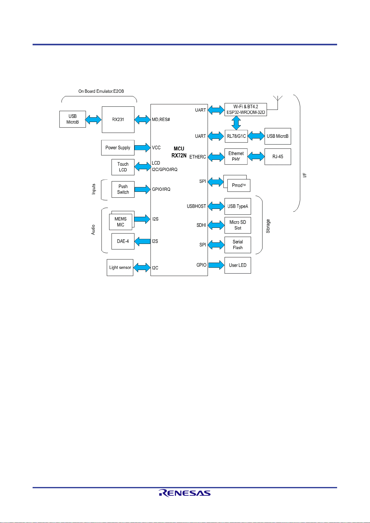
1.6 Block Diagram
Figure 1-1 is a block diagram of the product.
Figure 1-1. Block Diagram
Page 11
RX72N Envision Kit User's Manual 2. External View
R20UT4788EJ0100 Rev.1.00 Page 4 of 27
Mar.27.20
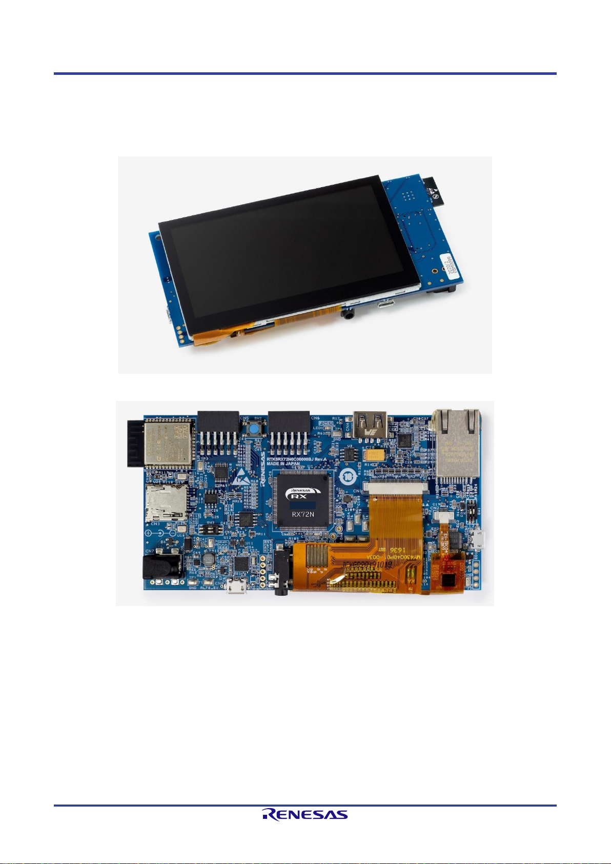
2. External View
Figure 2-1 is an external view of the LCD side of the product, Figure 2-2 is an external view of the component
side (as shipped from the factory), and Figure 2-3 is an external view of the component side (without LCD).
Figure 2-1. External View of LCD Side
Figure 2-2. External View of Component Side (as Shipped from the Factory)
Page 12
RX72N Envision Kit User's Manual 2. External View
R20UT4788EJ0100 Rev.1.00 Page 5 of 27
Mar.27.20
Figure 2-3. External View of Component Side (without LCD)
Page 13

RX72N Envision Kit User's Manual 3. Component Layout Diagram
R20UT4788EJ0100 Rev.1.00 Page 6 of 27
Mar.27.20
3. Component Layout Diagram
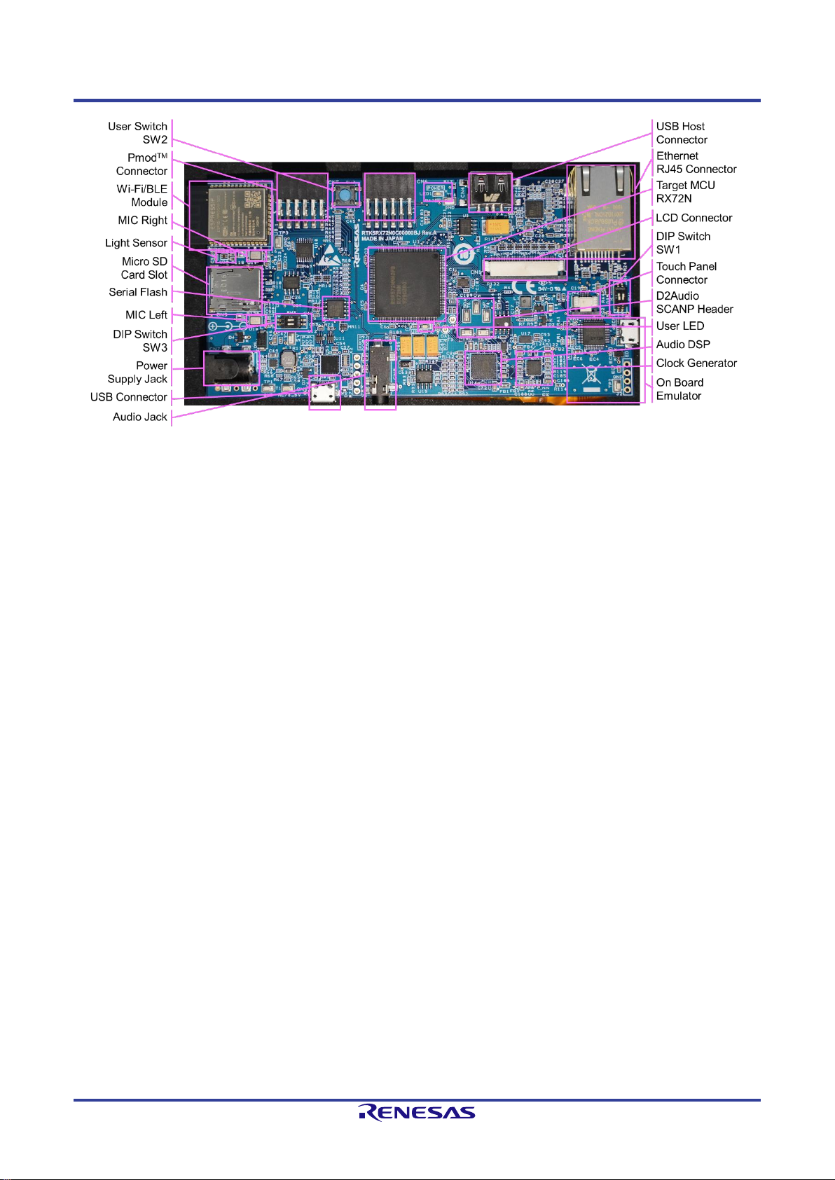
Figure 3-1 is a component layout diagram of the product.
Figure 3-1. Component Layout Diagram
Page 14

RX72N Envision Kit User's Manual 4. Operating Environment
R20UT4788EJ0100 Rev.1.00 Page 7 of 27
Mar.27.20
4. Operating Environment
Figure 4-1 shows the operating environment of the product. Install the integrated development environment
(IDE), available on the following webpage, on the host PC. The necessary drivers will be installed as part of
the IDE install process.
https://www.renesas.com/development-tools
Figure 4-1. Operating Environment
USB cable
Host PC
RX72N Envision Kit
Page 15

RX72N Envision Kit User's Manual 5. User Circuits
R20UT4788EJ0100 Rev.1.00 Page 8 of 27
Mar.27.20
5. User Circuits
5.1 Power Supply Circuit
The board operates on 5 V of power supplied via USB Micro-B connector ECN1 or DC jack CN7. Figure 5-1 is
a power supply system diagram.
Figure 5-1. RX72N Envision Kit Power Supply System Diagram
5.1.1 ECN1: USB Connector for On-Board Emulator
USB Micro-B connector ECN1 provides an interface for communication between the PC and a programmer or
emulator. Power is supplied to the board via the USB connector by default. Use of a USB port capable of
supplying at least 500 mA is recommended.
5.1.2 CN7: External Power Supply Connector
If the current capacity of the USB connector is insufficient, use CN7 (2.1 mm diameter connector, center +) to
supply power to the board. A voltage of 5.0 V can be supplied via this connector.
Figure 5-2. CN7 External Power Supply Connector Circuit
Page 16

RX72N Envision Kit User's Manual 5. User Circuits
R20UT4788EJ0100 Rev.1.00 Page 9 of 27
Mar.27.20
5.1.3 3.3 V Power supply
The MCU, Ethernet PHY, Wi-Fi/BLE module, etc., on the board operate on 3.3 V. A 3.3 V power supply is
generated from the 5 V power supply by the ISL80030 on-chip regulator with FET. Refer to the
www.renesas.com website for details of the ISL80030. Figure 5-3 shows the 3.3 V power supply circuit.
Figure 5-3. 3.3 V Power Supply Circuit
5.1.4 LCD Backlight Power Supply Circuit
The board is provided with an LCD backlight power supply to drive the backlight of the TFT LCD panel. The
backlight comprises a large number of white LEDs connected in series. (Since they share the same drive
current, uniform brightness is maintained.) The backlight requires 15 mA at 25 V while the board’s display is
operating. The ISL97634 is used to supply power to the backlight. Refer to the www.renesas.com website for
details of the ISL97634. Figure 5-4 shows the backlight power supply circuit.
Figure 5-4. LCD Backlight Power Supply Circuit
Page 17

RX72N Envision Kit User's Manual 5. User Circuits
R20UT4788EJ0100 Rev.1.00 Page 10 of 27
Mar.27.20
5.2 Reset Circuit
The board utilizes the power-on reset circuit incorporated into the MCU. For details of the MCU’s reset
specifications, refer to RX72N Group, RX72N Group User’s Manual: Hardware, and for details of the board’s
reset circuit, refer to the board circuit diagram.
5.3 Clock Circuit
The board is provided with a clock circuit for use as the clock source of the MCU. For details of the MCU’s
clock specifications, refer to RX72N Group User’s Manual: Hardware and RL78/G1C User’s Manual:
Hardware, and for details of the board’s clock circuit, refer to the board circuit diagram.
5.4 Evaluation MCU
As shipped from the factory, the power supply, system clock, and reset specifications of the evaluation MCU
are as follows:
• Power supply: Fixed at 3.3 V (including analog power supply)
• System clock: Operates on 16 MHz external oscillator
• Reset: Triggered by power-on reset
5.5 Emulator
The board is provided with an emulator. The emulator connector (ECN1) has a USB Micro-B configuration,
and it serves as an interface for the integrated development environment (IDE) and Renesas Flash
Programmer (RFP). Use a USB cable to connect the board to your PC. When the host PC is powered on,
power is supplied to the board via the USB cable connection.
Page 18

RX72N Envision Kit User's Manual 5. User Circuits
R20UT4788EJ0100 Rev.1.00 Page 11 of 27
Mar.27.20
5.6 DIP Switches
DIP switches SW1 and SW3 on the board are used to make a variety of settings. Figure 5-5 shows the
locations of the DIP switches, and Table 5-1 and Table 5-2 list the settings of each switch.
Figure 5-5. RX72N Envision Kit DIP Switches
Table 5-1. SW1 Settings
SW1
Function
Setting
1ch
Ethernet PHY reset
Off
PHY reset negate (default)
On
PHY reset assert
2ch
Emulator reset
Off
Emulator use enabled
On
Emulator reset (default)
Emulator use disabled
Table 5-2. SW3 Settings
SW3
Function
Setting
1ch
D2Audio reset
Off
D2Audio reset negate (default)
On
D2Audio reset assert
2ch
USB serial interface switching
Off
Connected to UART pins of MCU (default)
On
Connected to UART of Wi-Fi/BLE module
Note: Wi-Fi module download mode
Page 19

RX72N Envision Kit User's Manual 5. User Circuits
R20UT4788EJ0100 Rev.1.00 Page 12 of 27
Mar.27.20
5.7 USB Serial Interface
USB connector CN8 can be connected to the RL78/G1C and used as a virtual COM port. The USB serial
interface supports the following functions:
1. Evaluation MCU UART conversion, allowing connection via USB to a device such as a PC.
2. Connection to the ESP32-WROOM-32D Wi-Fi module, allowing programming of the on-chip flash memory
from a PC.
The RL78/G1C power supply (5 V) is isolated from other 5 V power supplies, so when using the above
functions it is necessary to connect an external power supply or plug a USB cable into ECN1.
Figure 5-6 and Table 5-3 illustrate USB serial connections.
Figure 5-6. USB Serial Interface
Table 5-3. USB Serial Interface
Signal
Function/Application
RX72N
Port
Pin
TXD
Transmit data signal
P13/TXD2
44
RXD
Receive data signal
P12/RXD2
45
When you first connect the board to a PC using the USB port, a message prompting you to install a driver
appears on the screen of the PC, as shown in Figure 5-7. After that, a message reporting that installation of
the driver is complete appears on the PC screen. The messages displayed may differ from those shown here
depending on the version of the operating system installed on the host PC.
Figure 5-7. USB Serial Driver Install Messages
If you do not have a copy of the driver installer, you can download it from the following webpage:
https://www.renesas.com/us/en/software/D6000699.html
BUS Swich
Level
Shifter
UVBUS
UDM0
UDP0
RxD0
TxD0
micro
USB
RL78_5V
RL78_5V3.3V
P13/TXD2
P12/RXD2
CN8
U9
RL78/G1C
1A
2A
S
1B1
1B2
2B1
2B2
SW3 2-3
To Wifi-module
Page 20

RX72N Envision Kit User's Manual 5. User Circuits
R20UT4788EJ0100 Rev.1.00 Page 13 of 27
Mar.27.20
5.8 Pmod™ Connectors
Connectors CN5 and CN6 are compliant with Pmod Interface Type 2A and provide connections to the
evaluation MCU.
Be careful not to bend or damage the pins when installing a Pmod™ module. The Pmod™ module is
susceptible to damage from electrostatic discharge (ESD). Therefore, protection against ESD is essential.
Figure 5-8 lists Pmod™ connector pin assignments, and Table 5-4 and Table 5-5 list the signal specifications
of the Pmod™ connectors. The connector numbering complies with the Digilent Pmod™ standard. For details,
refer to Digilent Pmod™ Interface Specification, Revision: November 20, 2011.
Figure 5-8. Pmod™ Connector Pin Assignments (Top View)
Table 5-4. Pmod™ Connector CN5 Pin Assignments
CN5
Pin No.
Signal
RX72N
CN5
Pin No.
Signal
RX72N
Port
Pin
Port
Pin
1
SS
P54
52 7 IRQ
P55
51 2 MOSI
P50
56 8 RST
P86
41 3 MISO
P52
54 9 IO0
P53
53 4 SCK
P51
55
10
IO1
P15
42 5 GND
⎯ ⎯ 11
GND
⎯ ⎯ 6
VCC
⎯ ⎯ 12
VCC
⎯
⎯
Table 5-5. Pmod™ Connector CN6 Pin Assignments
CN6
Pin No.
Signal
Evaluation MCU
CN6
Pin No.
Signal
Evaluation MCU
Port
Pin
Port
Pin
1
SS
P93
127 7 IRQ
PD0
126 2 MOSI
P90
131 8 RST
PD1
125 3 MISO
P92
128 9 IO0
P46
134 4 SCK
P91
129
10
IO1
P47
133 5 GND
⎯ ⎯ 11
GND
⎯ ⎯ 6
VCC
⎯ ⎯ 12
VCC
⎯
⎯
Page 21

RX72N Envision Kit User's Manual 5. User Circuits
R20UT4788EJ0100 Rev.1.00 Page 14 of 27
Mar.27.20
5.9 User Switch
The board is provided with a user switch (SW2) that you can utilize as you like. The user switch is connected
to the P107/IRQ15 port of the 144-pin evaluation MCU.
Figure 5-9. User Switch SW2
5.10 Wi-Fi/BLE Interface
The board is provided with the ESP32-WROOM-32D from Espressif Systems as its Wi-Fi module. It is
connected to the MCU via a UART.
Table 5-6. Wi-Fi Interface Pin Assignments
Signal
Function/Application
RX72N
Port
Pin
RXD
Transmit data signal
P26/TXD1
31
TXD
Receive data signal
P30/RXD1
29
CTS
Transmit enable
P27_RTS#
30
RTS
Transmit request
P31/CTS1#
28
EN
Wi-Fi enable
P43
137
5.10.1 Module Programming Settings
Switch Ch2 of SW3 on the board to the ON position to isolate the target MCU and enable a UART connection
to the USB serial interface in order to program the on-chip flash memory of the ESP32-WROOM-32D. For
instructions on programming the ESP32-WROOM-32D, visit the website of Espressif Systems.
Page 22

RX72N Envision Kit User's Manual 5. User Circuits
R20UT4788EJ0100 Rev.1.00 Page 15 of 27
Mar.27.20
5.11 Ethernet Interface
The board is provided with an Ethernet controller, which is connected to the MCU’s Ethernet module. The
MCU supports full-duplex and half-duplex modes and transfer rates of 10 Mbps and 100 Mbps. Table 5-7 lists
information related to Ethernet connections. Table 5-8 lists the states of the status LEDs.
Table 5-7. Ethernet
Signal
Function
RX72N
Port
Pin
ETXD3
4-bit transmit data
PC6/ET0_ETXD3
61
ETXD2
4-bit transmit data
PC5/ET0_ETXD2
62
ETXD1
4-bit transmit data
P82/ET0_ETXD1
63
ETXD0
4-bit transmit data
P81/ET0_ETXD0
64
TX_EN
Transmit enable
P80/ET0_TX_EN
65
TX_CLK
Transmit clock
PC4/ET0_TX_CLK
66
MDC
Management data clock
P72/ET0_MDC
85
MDIO
Management data serial I/O
P71/ET0_MDIO
86
ERXD3
4-bit receive data
PC0/ET0_ERXD3
75
ERXD2
4-bit receive data
PC1/ET0_ERXD2
73
ERXD1
4-bit receive data
P74/ET0_ERXD1
72
ERXD0
4-bit receive data
P75/ET0_ERXD0
71
RX_CLK
Receive clock
P76/ET0_RX_CLK
69
CRS
Carrier detect
P83/ET0_CRS
58
COL
Collision detect
PC7/ET0_COL
60
RX_DV
Receive data valid
PC2/ET0_RX_DV
70
RX_ER
Receive data error
P77/ET0_RX_ER
68
REFCLK
Reference clock
P56/CLKOUT25M
50
RES
PHY reset
P73_SW-PHYRESn
77
INTRP
Interrupt output
PC3_ET-INTn
67
Table 5-8. Ethernet Status LED States
Number
Green
Orange
State
1
Off
Off
Link broken
2
On (flashing)
Off
10 Mbps link state (data transmit/receive state)
3
On (flashing)
On
100 Mbps link state (data transmit/receive state)
Page 23

RX72N Envision Kit User's Manual 5. User Circuits
R20UT4788EJ0100 Rev.1.00 Page 16 of 27
Mar.27.20
5.12 microSD Slot
The microSD slot is connected to the MCU via the SDHI interface. The data bus width is wide bus (4-bit), and
compatible devices are SD memory cards (SD, SDHI, and SDXC) and SDIO cards.
Figure 5-10. microSD Slot Connection Diagram
Table 5-9. microSD Slot Pin Assignments
Signal
Function/Application
RX72N
Port
Pin
CLK
SDHI clock
P21/SDHI_CLK-C
36
CMD
Command output, response input
P20/SDHI_CMD-C
37
DATA0
Data 0
P22/SDHI_D0-C
35
DATA1
Data 1, SDIO access interrupt
P23/SDHI_D1-C
34
DATA2
Data 2, read wait
P87/SDHI_D2-C
39
CD/DATA3
Data 3, SD card detect
P17/SDHI_D3-C
38
SW_A
⎯ ⎯ ⎯
SW_B
SD card detect
P25/SDHI_CD
32
5.12.1 SDHI Power Supply Control
The SDHI power supply is connected to enable overcurrent monitoring by the MCU. The 3.3 V power supply
output to the SDHI is controlled by the evaluation MCU using the power management circuit in order to protect
against overloads and short circuits. This circuit is based on the ISL61861 power management IC. The IC has
an active-high enable input and (asserted low) fault output, and it can supply 3.3 V of power at up to 1.5 A.
Page 24

RX72N Envision Kit User's Manual 5. User Circuits
R20UT4788EJ0100 Rev.1.00 Page 17 of 27
Mar.27.20
5.13 USB Host Interface
The USB Host interface connects the evaluation MCU and the USB Host connector (type A). USB
connections to devices compatible with version 2.0 are supported. The supported transfer rates are full speed
(12 Mbps) and low speed (1.5 Mbps).
Table 5-10. USB Host Interface Pin Assignments
Signal
Function
RX72N
Port
Pin
USB0DP
D+ I/O signal
USB0_DP
48
USB0DM
D− I/O signal
USB0_DM
47
USB0VBUSEN
VBUS supply enable
P16_USB0_VBUSEN
40
USB0OVRCURA
Overcurrent detect
P14_USB0_OVR_CURA
43
5.13.1 USB Power Control
The USB power supply is connected to enable overcurrent monitoring by the MCU. The 5 V power supply
output to the USB Host is controlled by the evaluation MCU using the power management circuit in order to
protect against overloads and short circuits. A circuit diagram is shown in Figure 5-11. This circuit is based on
the ISL61861 power management IC. The IC has an active-high enable input and (asserted low) fault output,
and it can supply 5 V of power at up to 1.5 A.
Figure 5-11. USB Host Interface Connection Diagram
Page 25

RX72N Envision Kit User's Manual 5. User Circuits
R20UT4788EJ0100 Rev.1.00 Page 18 of 27
Mar.27.20
5.14 Serial Flash
The board is mounted with a MX25L3233F (32 Mbit) serial flash memory chip from MACRONIX. It is
connected to the MCU via the QSPI interface. It supports the MCU’s SPI operation modes 0 and 3.
Figure 5-12. Serial Flash Connection Diagram
Table 5-11. QSPI Serial Flash Pin Assignments
Signal
Function/Application
RX72N
Port
Pin
CS#
Chip select
PD4/QSSL
122
SO/SIO1
Data 1
PD7/QIO1
119
WP#/SIO2
Data 2
PD2/QIO2
124
SI/SIO0
Data 0
PD6/QIO0
120
SCLK
Clock supply
PD5/QSPCLK
121
HOLD#/SIO3
Data 3
PD3/QIO3
123
Page 26

RX72N Envision Kit User's Manual 5. User Circuits
R20UT4788EJ0100 Rev.1.00 Page 19 of 27
Mar.27.20
5.15 D2Audio Processor and Amplifier for Active Speaker
The D2Audio Series D2-41051 is used as the audio processor, and it is connected to the evaluation MCU via
the I2S interface. In addition, the board is provided with an amplifier circuit for use with an active speaker,
which can be connected to a speaker by means of a stereo jack to enable audio playback. The D2-41051
mounted on the board is a simple DSP that supports I2S and S/PDIF input and is limited to the basic functions
of the D2Audio family.
5.15.1 Speakers Suitable for Connection
You can connect an amplifier-equipped speaker to the audio output jack. It is also possible to connect an 8 Ω
speaker without an amplifier, but high-impedance devices such as headphones are not suitable for
connection.
5.15.2 Clock Supply
The board is provided with the 5X35023 programable clock generator that supplies a 24.576 MHz, 1.8 V clock
as the main clock of the D2-41051 and a 24.576 MHz, 3.3 V clock as AUDIO_CLK for I2S communication by
the RX72N.
5.15.3 DAE-4–Related Documents
The latest documents are available on the following webpage:
https://www.renesas.com/products/audio-video/audio/digital-sound-processors.html#documents
5.15.4 DAE-4 Development Tools
The development tools are available for download on the following webpage. Renesas would collect my
Renesas accounts for rights protection to manage who download the tool. Please note that anyone needs to
accept above to download.
https://www.renesas.com/products/audio-video/audio/digital-sound-processors.html#documents
5.15.5 DAE-4 Settings
The board’s default settings enable output of the PCM sound source input via I2S. The settings are stored in
the EEPROM, but if you need to reprogram the settings in the EEPROM because they were somehow erased
or in order to change them, it is possible to do so by purchasing the SCAMP-7EVALZ dongle tool, which is
available separately. In this case you will need to prepare yourself a cable with the pin assignments listed in
Table 5-12 to connect the SCAMP-7EVALZ to the board. To purchase the SCAMP-7EVALZ, contact a
Renesas sales agent or international distributor. You can search for a Renesas sales agent or distributor from
the following webpage:
https://www.renesas.com/support/contact/locations.html?category=Distributors
Page 27

RX72N Envision Kit User's Manual 5. User Circuits
R20UT4788EJ0100 Rev.1.00 Page 20 of 27
Mar.27.20
Table 5-12. Dongle Tool Connection Correspondences
Dongle (Female Socket)
EVB (IC Clip)
EEWP (12)
WP (T4)
SCL (3)
SCL (T5)
SDA (4)
SDA (T6)
BOOT_EE/I2C (11)
IRQA (T7)
EEWP (7)
RES (T8)
+5V (13)
5V (T9)
GND (14)
GND
Figure 5-13. Dongle Tool Connection Target
Page 28

RX72N Envision Kit User's Manual 5. User Circuits
R20UT4788EJ0100 Rev.1.00 Page 21 of 27
Mar.27.20
5.16 MEMS Microphones
The microphones used are the ICS-43434 from TDK, and they are connected to the evaluation MCU via the
I2S interface. Since the microphones for sound input are on the component side, sound is input from the panel
side.
Figure 5-14. MEMS Microphone Connection Diagram
Table 5-13. MEMS Microphone Pin Assignments
Signal
Function/Application
RX72N
Port
Pin
BCLK
I2S serial clock signal
P01/SSIBCK0
7
WS
Serial data select signal
PF5/SSILRCK0
9
DATA
I2S receive data signal
PJ5/SSIRXD0
11
Page 29

RX72N Envision Kit User's Manual 5. User Circuits
R20UT4788EJ0100 Rev.1.00 Page 22 of 27
Mar.27.20
5.17 Light Sensor
The ISL29034 is used as the light sensor, and it is connected to the evaluation MCU via the I2C interface.
Figure 5-15. Light Sensor Connection Diagram
Table 5-14. Light Sensor Pin Assignments
Signal
Function/Application
RX72N
Port
Pin
SCL
Transmit clock signal
PB6/SSCL11
79
SDA
Data signal
PB7/SSDA11
78
Page 30

RX72N Envision Kit User's Manual 5. User Circuits
R20UT4788EJ0100 Rev.1.00 Page 23 of 27
Mar.27.20
5.18 LEDs
There are five LEDs mounted on the board. Table 5-15 lists the colors and functions of the LEDs.
Table 5-15. LED Connection States
LED
Color
Function
RX72N
Port
Pin
LED1
Green
3.3 V power LED on: 3.3 V power supply status
NC
NC
ACT
Green
On-board debugger status
NC
NC
LED2
Blue
User LED
P40
141
ETHERNET connector
CN10
Green
Ethernet LED (on: link, flashing: activity)
NC
NC
Orange
Ethernet LED (speed)
NC
NC
Page 31

RX72N Envision Kit User's Manual 6. Usage Precautions
R20UT4788EJ0100 Rev.1.00 Page 24 of 27
Mar.27.20
6. Usage Precautions
6.1 Additional Load
When adding additional load while using the USB connection to supply power to the board, be aware that the
maximum capacity when operating at 3.3 V is 300 mA. When adding additional load while using an external
power supply, the maximum capacity is 500 mA regardless of the operating voltage.
6.2 Modifying the Board
All effects of modifications made to the board are the responsibility of the customer.
6.3 Limitation on Number of Envision Kits Connected
It is not possible to connect more than one Envision Kit to a single host PC at the same time.
Page 32

RX72N Envision Kit User's Manual 7. Developing Code
R20UT4788EJ0100 Rev.1.00 Page 25 of 27
Mar.27.20
7. Developing Code
7.1 Using e2 studio
Figure 7-1 shows the settings to use in e2 studio when creating a new project for use with the RX72N Envision
Kit.
• Debug hardware: Select E2 Lite (RX).
• Extal Frequency[MHz]: Input 16.000
• Connection Type: Select Fine.
• Supply power from emulator: Select No.
Figure 7-1. e2 studio Settings
Note: Do not connect another RX72N Envision Kit to the PC while the product is connected.
Page 33

RX72N Envision Kit User's Manual 7. Developing Code
R20UT4788EJ0100 Rev.1.00 Page 26 of 27
Mar.27.20
7.2 Using CS+
Figure 7-2 and Figure 7-3 show the settings to use in CS+ when creating a new project for use with the
RX72N Envision Kit.
• Debug tool used: Select Debug → Debug Tool Used → RX E2 Lite.
Figure 7-2. Debug Tool Selection Panel
• Main clock frequency[MHz]: Input 16.0000
• Supply power from emulator: Select No.
Figure 7-3. CS+ Connection Settings Tab
240.000
4,096
1,024
32
Page 34

RX72N Envision Kit User's Manual 8. Additional Information
R20UT4788EJ0100 Rev.1.00 Page 27 of 27
Mar.27.20
8. Additional Information
Support
For detailed information on RX72N Group MCUs, refer to RX72N Group User’s Manual: Hardware.
For detailed information on assembly language, refer to RX Family User’s Manual: Software.
The latest information is available on our website at https://www.renesas.com/envision2.
Online Technical Support
You may send technical questions to us via https://www.renesas.com/support/contact.html. For general
information on Renesas MCUs, visit https://www.renesas.com/.
Caution
Customers should not incorporate the RX72N Envision Kit or the sample code into their products. The
operation of the sample code is not guaranteed. If you wish to make use of it, be aware that it is the
customer’s responsibility to confirm that it operates properly.
Trademarks
All trademarks or registered trademarks appearing in this document are the property of their respective
owners.
Copyright
The contents of this document are subject to change in whole or in part without prior notice. This document is
copyright of Renesas Electronics Corporation. The contents of this document may not be copied in whole or in
part without the prior written approval of Renesas Electronics Corporation.
Page 35

Revision History
RX72N Envision Kit User’s Manual
Rev.
Date
Description
Page
Summary
1.00
Mar.27.20
⎯
First Edition issued
Page 36

RX72N Envision Kit User’s Manual
Publication Date: Rev.1.00 Mar.27.20
Published by: Renesas Electronics Corporation
Page 37

RX72N Group
R20UT4788EJ0100
 Loading...