

Page 1
RENESAS TECHNICAL UPDATE
TOYOSU FORESIA, 3-2-24, Toyosu, Koto-ku, Tokyo 135-0061, Japan
Renesas Electronics Corporation
Date: Apr. 2, 2021
Product
Category
Title
MPU/MCU
RX66N Group, RX72M Group, and RX72N Group,
Extension of Data Hold Time (Retention) of Flash
Memory
Document
No.
Information
Category
TN-RX*-A0251A/E
Technical Notification
Rev.
1.00
Lot No.
Applicable
Product
RX66N Group, RX72M Group,
RX72N Group
All
Reference
Document
User’s Manual: Hardware for applicable
products
(see the table at the last page)
This document describes the extension of the data hold time (retention) of the flash memory specified in the “Electrical
Characteristics” chapter of User’s Manual: Hardware for the applicable products.
Page and table numbers are based on the RX66N Group. Refer to the table on the last page for the corresponding page and table
numbers in the other groups.
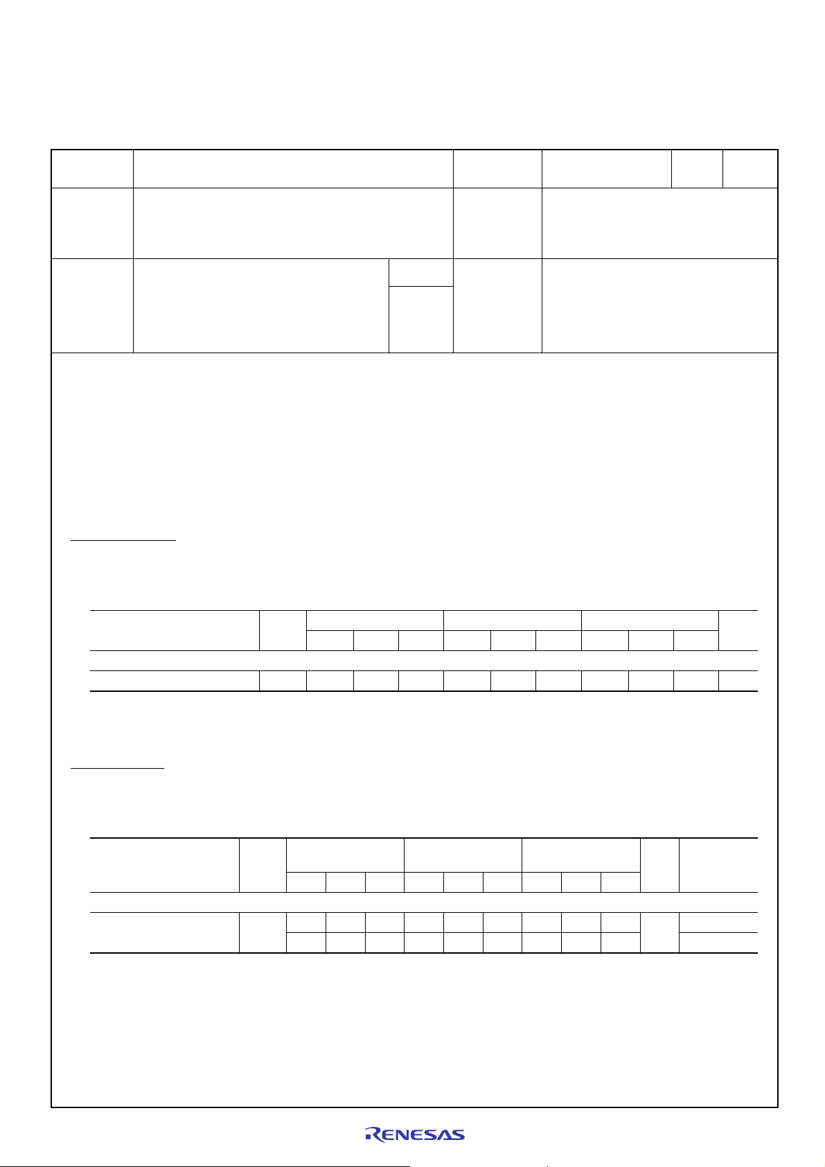
• Page 3034 of 3058
The specification of the data hold time in Table 61.61, Code Flash Memory Characteristics is changed as follows.
Before correction
Table 61.61 Code Flash Memory Characteristics
Conditions: Omitted.
Item Symbol
Data hold time*
Note 3. This shows the characteristics when the program/erase cycle does not exceed the specified value.
3
t
DRP
FCLK = 4 MHz FCLK = 15 MHz 20 MHz ≤ FCLK ≤ 60 MHz
Min. Typ. Max. Min. Typ. Max. Min. Typ. Max.
Omitted.
10 ——10 ——10 — — Year
Omitted.
After correction
Table 61.61 Code Flash Memory Characteristics
Conditions: Omitted.
Item Symbol
Data retention*
Note 3. This shows the characteristics when a self-programming library provided by Renesas Electronics or a flash programmer is used
Note 4. This result is obtained from reliability testing.
3, *4
and the program/erase cycle does not exceed the specified value.
t
DRP
FCLK = 4 MHz FCLK = 15 MHz
Min. Typ. Max. Min. Typ. Max. Min. Typ. Max.
Omitted.
20 ——20 ——20 — — Year Ta ≤ 85°C
10 ——10 ——10 —— T
Omitted.
20 MHz ≤ FCLK ≤
60 MHz
Unit Conditions
≤ 105°C
a
Unit
©2021. Renesas Electronics Corporation, All rights reserved. Page 1 of 2
Page 2
RENESAS TECHNICAL UPDATE TN-RX*-A0251A/E
Date: Apr. 2, 2021
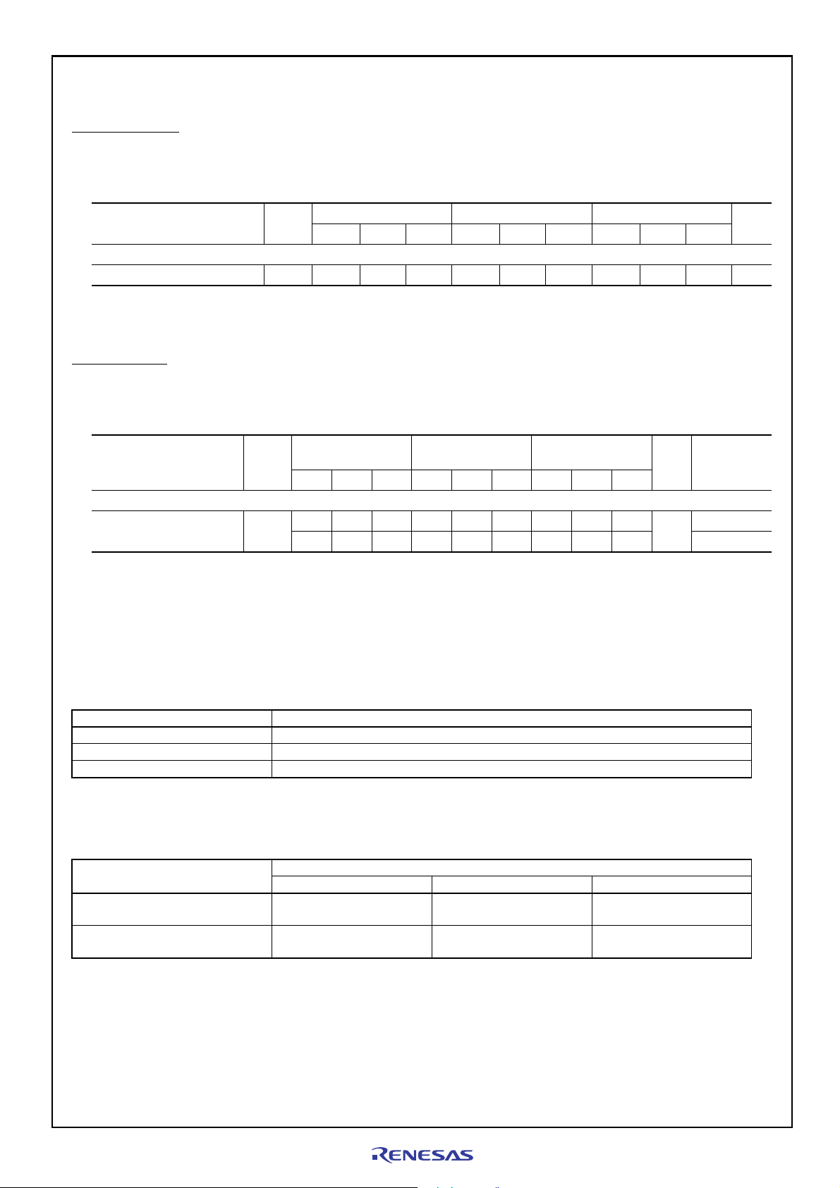
• Page 3035 of 3058
The specification of the data hold time in Table 61.62, Data Flash Memory Characteristics is changed as follows.
Before correction
Table 61.62 Data Flash Memory Characteristics
Conditions: Omitted.
Item Symbol
Data hold time*
Note 3. This shows the characteristics when the program/erase cycle does not exceed the specified value.
3
t
DRP
After correction
Table 61.62 Data Flash Memory Characteristics
Conditions: Omitted.
Item Symbol
Min. Typ. Max. Min. Typ. Max. Min. Typ. Max.
Data retention*
Note 3. This shows the characteristics when a self-programming library provided by Renesas Electronics or a flash programmer is used
Note 4. This result is obtained from reliability testing.
3, *4
and the program/erase cycle does not exceed the specified value.
t
DRP
FCLK = 4 MHz FCLK = 15 MHz 20 MHz ≤ FCLK ≤ 60 MHz
Min. Typ. Max. Min. Typ. Max. Min. Typ. Max.
Omitted.
10 ——10 ——10 — — Year
Omitted.
FCLK = 4 MHz FCLK = 15 MHz
Omitted.
20 ——20 ——20 — — Year Ta ≤ 85°C
10 ——10 ——10 —— T
Omitted.
20 MHz ≤ FCLK ≤
60 MHz
Unit Conditions
≤ 105°C
a
Unit
Reference Documents
Applicable Products Manual Title (Document Number)
RX66N Group RX66N Group User’s Manual: Hardware Rev1.11 (R01UH0825EJ0111)
RX72M Group RX72M Group User’s Manual: Hardware Rev1.11 (R01UH0804EJ0111)
RX72N Group RX72N Group User’s Manual: Hardware Rev1.11 (R01UH0824EJ0111)
Page Number, Section/Figure/Table Number
Item
Code flash memory characteristics
Data flash memory characteristics
RX66N Group RX72M Group RX72N Group
Page 3034 of 3058
Table 61.61
Page 3035 of 3058
Table 61.62
Page Number, Section/Figure/Table Number
Page 3339 of 3362
Table 65.63
Page 3340 of 3362
Table 65.64
Page 3208 of 3232
Table 63.61
Page 3209 of 3232
Table 63.62
Page 2 of 2
 Loading...