

Page 1
RENESAS TECHNICAL UPDATE
TOYOSU FORESIA, 3-2-24, Toyosu, Koto-ku, Tokyo 135-0061, Japan
Renesas Electronics Corporation
Date: Mar. 30, 2021
Product
Category
Title
MPU/MCU
RX65N Group and RX651 Group, Expansion of the
Lower Limit of the Power SupplyVoltage Supplied to
the Battery Backup Power Supply Pin
Document
No.
Information
Category
TN-RX*-A0250A/E
Technical Notification
Rev.
Lot No.
Applicable
Product
RX65N Group, RX651 Group
All
Reference
Document
RX65N Group, RX651 Group User’s
Manual: Hardware Rev.2.30
(R01UH0590EJ0230)
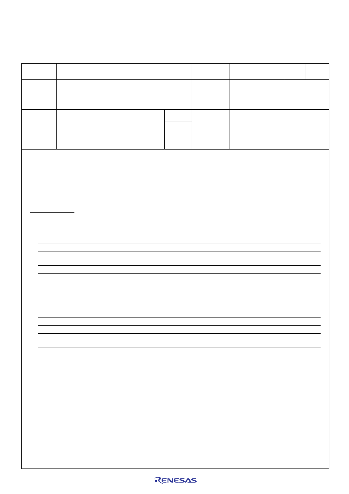
This document describes an extension of the lower limit of the power supply voltage supplied to the battery backup power
supply pin for the applicable products.
• Page 74 of 2729
The description for power supply voltage in Table 1.1, Outline of Specifications (10/10) is changed as follows.
Before correction
Table 1.1 Outline of Specifications (10/10)
Classification Module/Function Description
Omitted.
Power supply voltage VCC = AVCC0 = AVCC1 = VCC_USB = 2.7 to 3.6 V, 2.7 ≤ VREFH0 ≤ AVCC0,
= 2.0 to 3.6 V
V
BATT
Omitted.
1.00
After correction
Table 1.1 Outline of Specifications (10/10)
Classification Module/Function Description
Omitted.
Power supply voltage VCC = AVCC0 = AVCC1 = VCC_USB = 2.7 to 3.6 V, 2.7 ≤ VREFH0 ≤ AVCC0,
= 1.62 to 3.6 V*
V
BATT
Note 6. The low CL crystal unit cannot be used when the V
6
Omitted.
Omitted.
voltage is less than 2.0 V.
BATT
©2021. Renesas Electronics Corporation, All rights reserved. Page 1 of 5
Page 2
RENESAS TECHNICAL UPDATE TN-RX*-A0250A/E
• Page 2626 of 2729
The specification for V
Conditions are changed as follows.
Before correction
Table 60.2 Recommended Operating Conditions
V
power supply voltage V
BATT
Input voltage (5V tolerant ports 11 to 17, ports 20 and
21, ports 30 to 33, port 67, and ports C0 to C3)*
Note 4. For P32, P31, and P30, input as follows when the V
V
Min. = –0.3, Max. = V
in
After correction
power supply voltage and the description of Note 4 in Table 60.2, Recommended Operating
BATT
Item Symbol Min. Typ. Max. Unit
Omitted.
Omitted.
4
Omitted.
Omitted.
BATT
BATT
+ 0.3 (V
= 2.0 to 3.6 V)
BATT
BATT
V
in
2.0 —3.6V
–0.3 — VCC + 3.6 (up to 5.5) V
power supply is selected.
Date: Mar. 30, 2021
Table 60.2 Recommended Operating Conditions
Item Symbol Min. Typ. Max. Unit
Omitted.
V
power supply voltage V
BATT
BATT
1.62*
2
Omitted.
Input voltage (5V tolerant ports: P11 to P17, P20, P21,
P30 to P33, P67, and PC0 to PC3)*
5
V
in
–0.3 — VCC + 3.6 (up to 5.5) V
Omitted.
Omitted.
Note 2. The low CL crystal unit cannot be used when the V
voltage is less than 2.0 V.
BATT
Omitted.
Note 5. For P32, P31, and P30, input as follows when the V
V
Min. = –0.3, Max. = V
in
BATT
+ 0.3 (V
= 1.62 to 3.6 V)
BATT
power supply is selected.
BATT
• Page 2627 of 2729
The description of Note 3 in Table 60.3, DC Characteristics (1) is changed as follows.
Before correction
Note 3. For P32, P31, and P30, input as follows when the V
V
Min. = V
IH
× 0.8, VIL Max. = V
BATT
BATT
× 0.2 (V
power supply is selected.
BATT
= 2.0 to 3.6 V)
BATT
—3.6V
After correction
Note 3. For P32, P31, and P30, input as follows when the V
V
Min. = V
IH
× 0.8, VIL Max. = V
BATT
BATT
× 0.2 (V
power supply is selected.
BATT
= 1.62 to 3.6 V)
BATT
Page 2 of 5
Page 3

RENESAS TECHNICAL UPDATE TN-RX*-A0250A/E
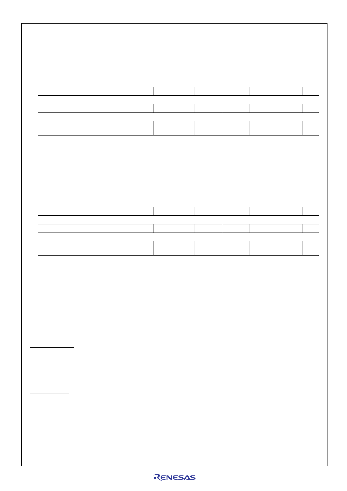
• Page 2629 of 2729
The characteristics of RTC operating current when a standard CL crystal is in use under the condition of V
added to Table 60.5, DC Characteristics (3) (P
Before correction
Table 60.5 DC Characteristics (3) (Products with 1 Mbyte of code flash memory or less)
Conditions: VCC = AVCC0 = AVCC1 = VCC_USB = 2.7 to 3.6 V, 2.7 V ≤ VREFH0 ≤ AVCC0,
VSS = AVSS0 = AVSS1 = VREFL0 = VSS_USB = 0 V,
T
= T
a
opr
Item Symbol
Supply
current*
1
When the RTC is
operating while VCC is
not supplied (Only the
RTC and sub-clock
oscillator operate with
the battery backup
function)
Omitted. ICC*
When a low C
use
When a standard C
is in use
roducts with 1 Mbyte of code flash memory or less) as follows.
crystal is in
L
crystal
L
D version G version
Typ. Max. Typ. Max.
3
0.9 — 0.9 — µA V
1.6 — 1.6 — V
1.7 — 1.7 — V
3.3 — 3.3 — V
Omitted.
Unit Test Conditions
Omitted.
Date: Mar. 30, 2021
= 1.62 V are
BATT
= 2.0 V,
BATT
VCC = 0 V
= 3.3 V,
BATT
VCC = 0 V
= 2.0 V,
BATT
VCC = 0 V
= 3.3 V,
BATT
VCC = 0 V
After correction
Table 60.5 DC Characteristics (3) (Products with 1 Mbyte of code flash memory or less)
Conditions: VCC = AVCC0 = AVCC1 = VCC_USB = 2.7 to 3.6 V, 2.7 V ≤ VREFH0 ≤ AVCC0,
VSS = AVSS0 = AVSS1 = VREFL0 = VSS_USB = 0 V,
T
= T
a
opr
D version G version
Typ. Max. Typ. Max.
3
0.9 — 0.9 — µA V
1.6 — 1.6 — V
1.6 — 1.6 — V
1.7 — 1.7 — V
3.3 — 3.3 — V
Supply
current*
1
When the RTC is
operating while VCC is
not supplied (Only the
RTC and sub-clock
oscillator operate with
the battery backup
function)
Item Symbol
Omitted. ICC*
When a low C
crystal is in
L
use
When a standard C
crystal
L
is in use
Omitted.
Unit Test Conditions
Omitted.
BATT
VCC = 0 V
BATT
VCC = 0 V
BATT
VCC = 0 V
BATT
VCC = 0 V
BATT
VCC = 0 V
= 2.0 V,
= 3.3 V,
= 1.62 V,
= 2.0 V,
= 3.3 V,
Page 3 of 5
Page 4

RENESAS TECHNICAL UPDATE TN-RX*-A0250A/E
Date: Mar. 30, 2021
• Page 2630 of 2729
The characteristics of RTC operating current when a standard CL crystal is in use under the condition of V
ed to Table 60.6, DC Characteristics (3) (Products for products with at least 1.5 Mbytes of code flash memory) as follows.
add
Before correction
Table 60.6 DC Characteristics (3) (Products for products with at least 1.5 Mbytes of code flash memory)
Conditions: VCC = AVCC0 = AVCC1 = VCC_USB = 2.7 to 3.6 V, 2.7 V ≤ VREFH0 ≤ AVCC0,
VSS = AVSS0 = AVSS1 = VREFL0 = VSS_USB = 0 V,
T
= T
a
opr
D version G version
Typ. Max. Typ. Max.
3
0.9 — 0.9 — µA V
1.6 — 1.6 — V
1.7 — 1.7 — V
3.3 — 3.3 — V
Unit Test Conditions
Omitted.
Supply
current*
1
When the RTC is
operating while VCC is
not supplied (Only the
RTC and sub-clock
oscillator operate with
the battery backup
function)
Item Symbol
Omitted. ICC*
When a low C
crystal is in
L
use
When a standard C
crystal
L
is in use
Omitted.
= 1.62 V are
BATT
= 2.0 V,
BATT
VCC = 0 V
= 3.3 V,
BATT
VCC = 0 V
= 2.0 V,
BATT
VCC = 0 V
= 3.3 V,
BATT
VCC = 0 V
After correction
Table 60.6 DC Characteristics (3) (Products with at least 1.5 Mbytes of code flash memory)
Conditions: VCC = AVCC0 = AVCC1 = VCC_USB = 2.7 to 3.6 V, 2.7 V ≤ VREFH0 ≤ AVCC0,
VSS = AVSS0 = AVSS1 = VREFL0 = VSS_USB = 0 V,
T
= T
a
opr
D version G version
Typ. Max. Typ. Max.
3
0.9 — 0.9 — µA V
1.6 — 1.6 — V
1.6 — 1.6 — V
1.7 — 1.7 — V
3.3 — 3.3 — V
Omitted.
Supply
current*
1
When the RTC is
operating while VCC is
not supplied (Only the
RTC and sub-clock
oscillator operate with
the battery backup
function)
Item Symbol
Omitted. ICC*
When a low C
crystal is in
L
use
When a standard C
crystal
L
is in use
Omitted.
Unit Test Conditions
= 2.0 V,
BATT
VCC = 0 V
= 3.3 V,
BATT
VCC = 0 V
= 1.62 V,
BATT
VCC = 0 V
= 2.0 V,
BATT
VCC = 0 V
= 3.3 V,
BATT
VCC = 0 V
Page 4 of 5
Page 5

RENESAS TECHNICAL UPDATE TN-RX*-A0250A/E
• Page 2641 of 2729
The V
Before correction
Table 60.20 Sub-Clock Timing
Conditions: VCC = AVCC0 = AVCC1 = VCC_USB = 2.7 to 3.6 V, 2.7 V ≤ VREFH0 ≤ AVCC0,
After correction
Table 60.20 Sub-Clock Timing
Conditions: VCC = AVCC0 = AVCC1 = VCC_USB = 2.7 to 3.6 V, 2.7 V ≤ VREFH0 ≤ AVCC0,
voltage in Conditions of Table 60.20, Sub-Clock Timing is changed as follows.
BATT
VSS = AVSS0 = AVSS1 = VREFL0 = VSS_USB = 0 V,
V
= 2.0 to 3.6 V, Ta = T
BATT
VSS = AVSS0 = AVSS1 = VREFL0 = VSS_USB = 0 V,
V
= 1.62 to 3.6 V, Ta = T
BATT
opr
opr
• Page 2700 of 2729
The V
Before correction
voltage in Conditions of Table 60.55, Battery Backup Function Characteristics is changed as follows.
BATT
Date: Mar. 30, 2021
Table 60.55 Battery Backup Function Characteristics
Conditions: VCC = AVCC0 = AVCC1 = VCC_USB = 2.7 to 3.6 V, 2.7 V ≤ VREFH0 ≤ AVCC0,
VSS = AVSS0 = AVSS1 = VREFL0 = VSS_USB = 0 V,
V
= 2.0 to 3.6 V, Ta = T
BATT
opr
After correction
Table 60.55 Battery Backup Function Characteristics
Conditions: VCC = AVCC0 = AVCC1 = VCC_USB = 2.7 to 3.6 V, 2.7 V ≤ VREFH0 ≤ AVCC0,
VSS = AVSS0 = AVSS1 = VREFL0 = VSS_USB = 0 V,
V
= 1.62 to 3.6 V, Ta = T
BATT
opr
Page 5 of 5
 Loading...