

Page 1

Renesas Electronics
R-IN32M3 Series
edition
・
・
User's Manual
User’s Manual: Board design
R-IN32M3-EC
R-IN32M3-CL
All information contained in these materials, including products and product specifications, represents
information on the product at the time of publication and is subject to change by Renesas Electronics
Corp. without notice. Please review the latest information published by Renesas Electronics Corp.
through various means, including the Renesas Electronics Corp. website (http://www.renesas.com)
Document number: R18UZ0021EJ0400
Issue date: Dec. 28, 2018
www.renesas.com
Page 2

Notice
1. Descriptions of circuits, software and other related information in this document are provided only to illustrate the
operation of semiconductor products and application examples. You are fully responsible for the incorporation of these
circuits, software, and information in the design of your equipment. Renesas Electronics assumes no responsibility for
any losses incurred by you or third parties arising from the use of these circuits, software, or information.
2. Renesas Electronics has used reasonable care in preparing the information included in this document, but Renesas
Electronics does not warrant that such information is error free. Renesas Electronics assumes no liability whatsoever
for any damages incurred by you resulting from errors in or omissions from the information included herein.
3. Renesas Electronics does not assume any liability for infringement of patents, copyrights, or other intellectual property
rights of third parties by or arising from the use of Renesas Electronics products or technical information described in
this document. No license, express, implied or otherwise, is granted hereby under any patents, copyrights or other
intellectual property rights of Renesas Electronics or others.
4. You should not alter, modify, copy, or otherwise misappropriate any Renesas Electronics product, whether in whole or
in part. Renesas Electronics assumes no responsibility for any losses incurred by you or third parties arising from such
alteration, modification, copy or otherwise misappropriation of Renesas Electronics product.
5. Renesas Electronics products are classified according to the following two quality grades: "Standard" and "High
Quality". The recommended applications for each Renesas Electronics product depends on the product's quality grade,
as indicated below.
"Standard": Computers; office equipment; communications equipment; test and measurement equipment; audio
and visual equipment; home electronic appliances; machine tools; personal electronic equipment;
and industrial robots etc.
"High Quality": Transportation equipment (automobiles, trains, ships, etc.); traffic control systems; anti-disaster
systems; anti-crime systems; and safety equipment et c.
Renesas Electronics products are neither intended nor authorized for use in products or systems that may pose a
direct threat to human life or bodily injury (artificial life support devices or systems, surgical implantations etc.), or may
cause serious property damages (nuclear reactor control systems, military equipment etc.). You must check the quality
grade of each Renesas Electronics product before using it in a particular application. You may not use any Renesas
Electronics product for any application for which it is not intended. Renesas Electronics shall not be in any way liable
for any damages or losses incurred by you or third parties arising from the use of any Renesas Electronics product for
which the product is not intended by Renesas Electro ni cs.
6. You should use the Renesas Electronics products described in this document within the range specified by Renesas
Electronics, especially with respect to the maximum rating, operating supply voltage range, movement power voltage
range, heat radiation characteristics, installation and other product characteristics. Renesas Electronics shall have no
liability for malfunctions or damages arising out of the use of Renesas Electronics products beyond such specified
ranges.
7. Although Renesas Electronics endeavors to improve the quality and reliability of its products, semiconductor products
have specific characteristics such as the occurrence of failure at a certain rate and malfunctions under certain use
conditions. Further, Renesas Electronics products are not subject to radiation resistance design. Please be sure to
implement safety measures to guard them against the possibility of physical injury, and injury or damage caused by
fire in the event of the failure of a Renesas Electronics product, such as safety design for hardware and software
including but not limited to redundancy, fire control and malfunction prevention, appropriate treatment for aging
degradation or any other appropriate measures. Because the evaluation of microcomputer software alone is very
difficult, please evaluate the safety of the final products or systems manufactured by you.
8. Please contact a Renesas Electronics sales office for details as to environmental matters such as the environmental
compatibility of each Renesas Electronics product. Please use Renesas Electronics products in compliance with all
applicable laws and regulations that regulate the inclusion or use of controlled substances, including without limitation,
the EU RoHS Directive. Renesas Electronics assumes no liability for damages or losses occurring as a result of your
noncompliance with applicable laws and regulations.
9. Renesas Electronics products and technology may not be used for or incorporated into any products or systems
whose manufacture, use, or sale is prohibited under any applicable domestic or fore ign la ws or regulations. You
should not use Renesas Electronics products or technology described in this document for any purpose relating to
military applications or use by the military, including but not limited to the development of weapons of mass destruction.
When exporting the Renesas Electronics products or technology described in this document, you should comply with
the applicable export control laws and regulations and follow the procedures required by such laws and regulations.
10. It is the responsibility of the buyer or distributor of Renesas Electronics products, who distributes, disposes of, or
otherwise places the product with a third party, to notify such third party in advance of the contents and conditions set
forth in this document, Renesas Electronics assumes no responsibility for any losses incurred by you or third parties as
a result of unauthorized use of Renesas Electronics products.
11. This document may not be reproduced or duplicated in any form, in whole or in part, without prior written consent of
Renesas Electronics.
12. Please contact a Renesas Electronics sales office if you have any questions regarding the information contained in this
document or Renesas Electronics products, or if you have any other inquiries.
(Note 1) "Renesas Electronics" as used in this document means Renesas Electronics Corporation and also includes its
majority-owned subsidiaries.
(Note 2) "Renesas Electronics product(s)" means any product developed or manufactured by or for Renesas Electronics.
Page 3

Arm® and Cortex® are registered trademarks of Arm Limited (or its subsidiaries) in the EU and/or elsewhere.
belongs to the respective owners.
Instructions for the use o f product
In this section, the precautions are described for over whole of CMOS device.
Please refer to this manual about individual precaution.
When there i s a mention unlike the text of this manual, a mention of the text takes first priority.
1.Handling of Unused Pins
Handle unused pins in accord with the directions given under Handling of Unused Pins in the manual.
- The input pins of CMOS products are generally in the high-impedance state. In operation w ith an unused pin in
the open-circuit state, extra electromagnetic noise is induced in the vicinity of LSI, associated shoot-through
current flows internally, and malfun cti ons occur due to the false recognition of the pin state as an input signal
become possible. Unused pins should be h and led as descr i b ed under Ha ndl ing of Unu sed Pins in the manu al.
2. Processing at Power-on
The state of the product is undefined at the moment when power is supplied.
- The states of internal circuits in the LSI are indeterminate and the states of register sett in gs and pins are
undefined at the moment when power is supplied.
In a finished product where the reset signal is applied to the external reset pin, the states of pins are not
guaranteed from the moment when power is supplied until the reset process is completed.
In a similar way, the states of pins in a product that is reset by an on-chip power-on reset function are not
guaranteed from the moment when power is supplied until the power reaches the level at which resetting has
been specified.
3. Prohibition of Access to Reserved Addresses
Access to reserved addresses is prohibited.
- The reserved addresses are provided for the possible future expansion of functions. Do not access these
addresses; the correct operation of LSI is not guaranteed if they are accessed.
4. Clock Signals
After applying a reset, only release the reset line after the operating clock signal has become stable. When
switching the clock signal during program execution, wait until the target clock signal has stabilized.
- When the clock signal is generated with an external resonator (or from an external oscillator) during a reset,
ensure that the reset line is only released after full stabilization of the clock signal. Moreover, when switching to
a clock signal produced with an external resonator (or by an external oscillator) while program execution is in
progress, wait until the target clock signal is stable.
・
All rights reserved.
・Ethernet is a registered trademark of Fuji Xerox Co., Ltd.
・IEEE is a registered trademark of the Institute of Electrical and Electronics Engineers Inc.
・TRON is an acronym for "The Real-time Operation system Nucleus".
・ITRON is an acronym for "Industrial TRON".
・µITRON is an acronym for "Micro Industrial TRON".
・TRON, ITRON, and µITRON do not refer to any specific product or products.
・EtherCAT
GmbH, Germany.
・CC-Link and CC-Link IE Field are registered trademarks of the CC-Link Partner Association (CLPA).
Additionally all product names and service names in this document are a trademark or a registered trademark which
・
®
and TwinCAT® are registered trademark and patented technology, licensed by Beckhoff Automation
Page 4

Particular attention should be paid to the precautionary notes when using the manual. These notes occur
within the body of the text, at the end of each section, and in the Usage Notes section.
The revision history summarizes the locations of revisions and additions. It does not list all revisions. Refer
point in this document.
refer to it.
Document Name
Document Number
R-IN32M3 Series Datasheet
R18DS0008EJ****
R-IN32M3 Series User’s Manual R-IN32M3-EC
R18UZ0003EJ****
R-IN32M3 Series User’s Manual R-IN32M3-CL
R18UZ0005EJ****
R-IN32M3 Series User’s Manual: Peripheral Modules
R18UZ0007EJ****
R-IN32M3 Series Programming Manual: Driver
R18UZ0009EJ****
R-IN32M3 Series Programming Manual: OS
R18UZ0011EJ****
R-IN32M3 Series User’s Manual Peripheral: Board design edition
This manual
How to use this manual
1. Purpose and Target Readers
This manual is intended for users who wish to understand the functions of Industrial Ethernet network LSI
"R-IN32M3-EC/CL" for designing application of it. It is assumed that the reader of this manual has general knowledge in
the fields of electrical engineering, logic circuits, and microcontrollers.
to the text of the manual for details.
The mark "<R>" means the updated point in this revision. The mark "<R>" let users search for the updated
Related
Documents
The related documents indicated in this public ation may include preliminary versions. However,
preliminary versions a re not marked as such. Please be understanding of this beforehand. In addition,
because we make document at development, planning of each core, the related document may be the
document for individual customers. Last four digits of document number (described as ****) indicate
version information of each document. Please download the latest document from our web site and
The document related to R-IN32M3 Series
Page 5

2. Not at ion of Numbers and Symbols
Weight in data notation: Left is high-order column, right is low-order column
Active low notation:
xxxZ (capital letter Z after pin name or signal name)
or xxx_N (capital letter _N after pin name or signal name)
or xxnx (pin name or signa l name contains small letter n)
Note:
explanation of (Note) in the text
Caution:
Item deserving extra attention
Remark:
Supplementary explanation to the text
Numeric notation:
Binary: xxxx , xxxxB or n’bxxxx (n bits)
Decimal: xxxx
Hexadecimal: xxxxH or n’hxxxx (n bits)
Prefixes representing powers of 2 (address space, memory capacity):
K (kilo): 2
M (mega): 2
G (giga): 2
Data Type:
Word: 32 bits
Halfword: 16 bits
Byte: 8 bits
10
= 1024
20
= 10242
30
= 10243
Page 6

Contents
1. Outline ........................................................................................................................................................... 1
1.1 Definitio n of Pin Hand ling and Symbols in This Manual ................................................................................... 1
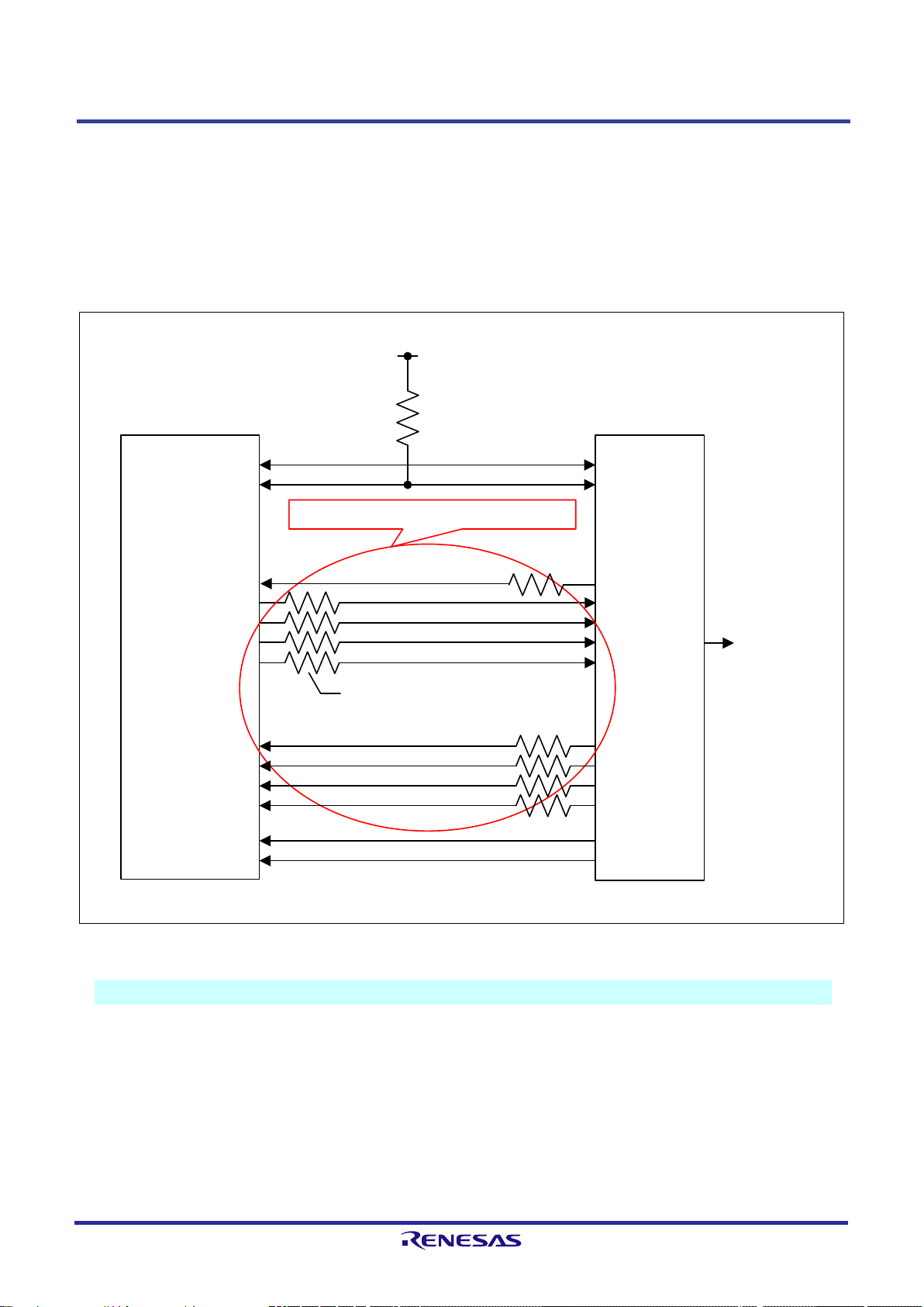
2. Power/Reset Pins .......................................................................................................................................... 2
2.1 Power-O n/O ff Se q ue nc e ..................................................................................................................................... 2
2.2 Power Supply Pins .............................................................................................................................................. 3
2.3 Reset Pins ........................................................................................................................................................... 4
3. Clock Input Pins ............................................................................................................................................. 5
3.1 Features of Pins ................................................................................................................................................... 5
3.2 Notes on Configuring the Oscillation Circuit ..................................................................................................... 6
3.3 Oscillation Circuit Configurati on Example ........................................................................................................ 7
4. PLL Power Pins ............................................................................................................................................. 8
4.1 Recommended Configuration of Filter ............................................................................................................... 8
4.2 Notes on Placement of Peripheral Components .................................................................................................. 9
5. Built-in Regulator Pin (R-IN32M3-EC only) ................................................................................................. 10
5.1 Built-in Regulator Used .................................................................................................................................... 10
5.2 Built-in Regulator Unused ................................................................................................................................ 12
6. GPIO Port Pins ............................................................................................................................................ 13
7. Ethernet PHY Pins (R-IN32M3-EC Only) .................................................................................................... 14
7.1 Ethernet PH Y Power Supply Pins ..................................................................................................................... 14
7.2 100Base-TX Pins .............................................................................................................................................. 15
7.3 100Base-FX Pins (Optical Fiber)...................................................................................................................... 19
8. GMII Pins (R-IN32M3-CL Only) ................................................................................................................... 20
8.1 Selection of GMII Peripheral Components ....................................................................................................... 21
8.2 Circuit Design around GMII ............................................................................................................................. 21
8.3 Pattern Design around GMII ............................................................................................................................. 21
Contents-1
Page 7

9. CC-Link Pins ................................................................................................................................................ 22
10. Notes of CC-Link IE Field Use (Only R-IN32M3-CL) .................................................................................. 24
11. External MCU/Memory Interface Pins ......................................................................................................... 25
11.1 External MCU Interface .................................................................................................................................... 26
11.1.1 Asynchronous SRAM Interface Mode ..................................................................................................... 27
11.1.2 Synchronous SRAM Interface Mode ....................................................................................................... 29
11.1.3 Synchronous SRAM-Type Transfer Mode .............................................................................................. 30
11.2 External Memory Interface ............................................................................................................................... 31
11.2.1 Asynchronous SRAM MEMC ................................................................................................................. 31
11.2.2 Synchronous Burst Access MEM C ......................................................................................................... 34
12. Serial Flash ROM Connection Pins ............................................................................................................. 37
13. As ynchro nous Ser i al Interf ac e J Connec ti on Pins ...................................................................................... 38
14. I2C Connection Pins..................................................................................................................................... 39
15. EtherCAT EEPROM I2C Connection Pins (R-IN32M3-EC Only) ................................................................ 40
16. CAN Pi ns ..................................................................................................................................................... 41
17. CSIH Pins <R> ............................................................................................................................................ 42
17.1 One Master and One Slave ............................................................................................................................... 42
17.2 One Master and Two Slaves ............................................................................................................................. 42
18. JTAG/Trace Pins ......................................................................................................................................... 43
19. Implementation Conditions .......................................................................................................................... 46
20. Package Information .................................................................................................................................... 47
21. Mount Pad Information ................................................................................................................................ 48
22. BSCAN Information ..................................................................................................................................... 49
22.1 BSCAN Operating Conditions .......................................................................................................................... 49
22.2 Maximum Operating Frequency of TCK .......................................................................................................... 49
22.3 IDCODE ........................................................................................................................................................... 49
22.4 BSCAN Non-Supported Pins ............................................................................................................................ 50
Contents-2
Page 8

22.5 How to Get BSDL ............................................................................................................................................ 51
22.6 Notes on Using BSDL <R> .............................................................................................................................. 51
23. IBIS Information ........................................................................................................................................... 52
24. Marking Information ..................................................................................................................................... 53
24.1 R-IN32M3-EC .................................................................................................................................................. 53
24.2 R-IN32M3-CL .................................................................................................................................................. 53
25. Thermal Design <R> ................................................................................................................................... 54
25.1 Deciding on whether Particular Measures for Heat Dissipation are Required .................................................. 54
25.1.1 Estimating Tj ........................................................................................................................................... 54
25.1.2 Estimating Power Consumptio n .............................................................................................................. 54
25.1.3 Thermal Resistances under the JEDEC Conditions (for θja and Ψjt) ...................................................... 55
25.1.4 Results of Estimating Power Consumption of the 1-V Sub-Systems at Tj .............................................. 55
25.1.5 Relation between Temperature Increases (∆t) and Thermal Resistance (θja) at a Given Ambient
Temperature ............................................................................................................................................. 57
25.2 Examples of Measures for Heat Dissipation ..................................................................................................... 58
25.2.1 Measures for Heat Release in Designing the Board ................................................................................. 59
25.2.2 Heat Dissipation from the Per iphery (Including the Casing) ................................................................... 61
25.3 Points for Caution ............................................................................................................................................. 62
25.3.1 Internal Regulator .................................................................................................................................... 62
25.3.2 Handling of Unused Pins ......................................................................................................................... 62
26. Countermeasure for Noise <R> .................................................................................................................. 64
26.1 Stopping Cl ock Output ..................................................................................................................................... 64
Contents-3
Page 9

List of Figures
Figure 1.1
Figure 2.1 Recommended Sequence of Power-On/Off .......................................................................................... 2
Figure 3.1 Example of GND Pat tern for the Components for External Constants ................................................. 6
Figure 3.2 Configuration Example of the Oscillation Circuit ................................................................................ 7
Figure 4.1 Recommended Configuration of Filter ................................................................................................. 8
Figure 4.2 Schematic View from Below the Board ................................................................................................ 9
Figure 5.1 Wiring Example of the Regulator Unit (Built-in Regulator Used) ..................................................... 10
Figure 5.2 Layout Example of the Regulator Section .......................................................................................... 11
Figure 5.3 Wiring Exa mple of the Regulator Unit (Internal Regulator is Not Used) ........................................... 12
Figure 7.1 Decoupling Capacitors for Power Supply ........................................................................................... 14
Figure 7.2 Connection Example of R-IN32M3-EC and RJ-45 Connector (Pulse Transformer Incorporated) ..... 15
Figure 7.3 Connection Example of R-IN32M3-EC, Pulse Transformer, and RJ-45 Connector........................... 16
Figure 7.4 Wiring Example of the Differential Signal Trans mission Line (1) ..................................................... 17
Figure 7.5 Wiring Example of the Differential Signal Transmissio n Line (2) ..................................................... 18
Figure 7.6 Wiring Example of the Differential Signal Trans mission Line (3) ..................................................... 18
Figure 7.7 Interface Circuit with Optica l Transceiver .......................................................................................... 19
Figure 8.1 Connection Image of R-IN32M3-CL and Gigabit Ethernet PHY ....................................................... 20
Figure 9.1 Connection Example for CC-Link Remote Device Station ................................................................ 23
Figure 11.1 Connection Example of 32-Bit External MCU Interface (Asynchronous SRAM Interface Mode) .... 27
Figure 11.2 Connection Example of 16-Bit External MCU Interface (Asynchronous SRAM Interface Mode) .... 27
Figure 11.3 Connection Example of 32-Bit External MCU Interface (Synchronous SRAM Interface Mode) ...... 29
Figure 11.4 Connection Example of 16-Bit External MCU Interface (Synchronous SRAM Interface Mode) ...... 29
Figure 11.5 Connection Example of 32-Bit External MCU Interface (Synchronous SRAM-Type Transfer
Figure 11.6 Connection Example of 16-Bit External MCU Interface (Synchronous SRAM-Type Transfer
Figure 11.7 Connection Example with 32-Bit SRAM (Asynchronous SRAM MEMC) ........................................ 32
Figure 11.8 Connection Example with 16-Bit SRAM (Asynchronous SRAM MEMC) ........................................ 32
Figure 11.9 Connection Example with 32-Bit Paged ROM (Asynchronous SRAM MEMC) ............................... 33
Figure 11.10 Connection Example with 16-Bit Paged ROM (Asynchronous SRAM MEMC) .............................. 33
Figure 11.11 Connection Example with 32-Bit SRAM (Synchronous Burst Access MEMC) ............................... 35
Figure 11.12 Connection Example with 16-Bit SRAM (Synchronous Burst Access MEMC) ............................... 35
Figure 11.13 Connection Example with 32-Bit Paged RO M (Synchronous Burst Acc ess MEMC) ....................... 36
Figure 11.14 Connection Example with 16-Bit Paged ROM (Synchronous Burst Access MEMC) ....................... 36
Figure 12.1 Connection Example with Serial Flash ROM <R> ............................................................................. 37
Figure 13.1 Connection Example between R-IN32M3 and UART Device ........................................................... 38
Figure 14.1 Connection Example between R-IN32M3 and I2C Slave Device ....................................................... 39
Figure 15.1 Connection Example between R-IN32M3-EC and EtherCAT EEPROM .......................................... 40
Figure 16.1 Connection Example between R-IN32M3 and CAN Transceiver ...................................................... 41
Figure 17.1 Direct Master/Slave Connection ......................................................................................................... 42
Definition of GND Symbols ................................................................................................................. 1
Mode) .................................................................................................................................................. 30
Mode) ................................................................................................................................................. 30
Contents-4
Page 10

Figure 17.2 Connection between One Master and Two Slaves .............................................................................. 42
Figure 18.1 Connection Example of JTAG Interface (20-Pin Half-Pitch without Trace) ...................................... 43
Figure 18.2 Connection Example of JTAG Interface (20-Pin Half-Pitch with T race) ........................................... 44
Figure 18.3 Connection Example of JTAG Interface (20-Pin Full-Pitch) .............................................................. 45
Figure 19.1 Implementation Flow .......................................................................................................................... 46
Figure 19.2 Infrared Reflow Temperature Profile .................................................................................................. 46
Figure 20.1 Package Information ........................................................................................................................... 47
Figure 21.1 Mount Pad Sizes ................................................................................................................................. 48
Figure 24.1 R-IN32M3-EC Marking Info rmation .................................................................................................. 53
Figure 24.2 R-IN32M3-CL Marking Info rmation .................................................................................................. 53
Contents-5
Page 11

List of Tables
Table 1.1
Table 5.1 List of Recommended Parts for Use ....................................................................................................... 11
Table 7.1 Parts List (100Base-TX interface) .......................................................................................................... 16
Table 7.2 Part List (100Base-FX Interface) ............................................................................................................ 19
Table 11.1 Mode Selection of External MCU/Memory Connection..................................................................... 25
Table 22.1 List of BSCAN No n-Supported Pins<R> ........................................................................................... 50
Definition of Pin Handling ........................................................................................................................ 1
Contents-6
Page 12

Description
Low level
This pin is connected to GND.
High level
This pin supplies VDD33 (3.3 V).
Frame GNDAnalog GND
GND
R18UZ0021EJ0400
R-IN32M3 Series: Board design edition Dec. 28, 2018
1. Outline
This manual is intended for being us ed by engi neers that work on a circuit and P C B design that is equipp ed with an
Ethernet communication LSI from the R-IN32M3 series made by Renesas Electronics. Target devices are the
R-IN32M3-EC and R-IN32M3-CL devices.
It is recommended to st udy this manual caref ully and to fo l low the recommendati ons during the circui t and boa rd design.
1.1 Definition o f Pin Handling and Symbols in This Manual
Pin handling and symbols are defined as follows in this manual.
Table 1.1 Definition of Pin Handling
Figure 1.1 Definition of GND Symbols
R18UZ0021EJ0400 Page 1 of 64
Dec. 28, 2018
Page 13

R-IN32M3 Series: Board design edition 2. Power/Reset Pins
I/O voltage
(VDD33)
100ms
0.1 VDD10
GND
Internal voltage
(VDD10)
100ms
0.1 VDD10
0.9 VDD33
PHY voltage
Note
(VDD15)
.
The timing for PHY power supply voltage VDD15 only needs to be observed, when the internal
regulator in the R-IN32M3-EC device is not used.
2. Power/Reset Pins
2.1 Power-On/Off Sequence
Power structure of the R-IN32M3 series is internal power (VDD10: 1.0V) and I/O power (VDD33: 3.3V) and PHY
power supply (VDD15: 1.5V). (PHY power is subject only R-IN32M3-EC.)
Power is recommended to put the I/O p ower after switching on the internal power supply. In addition, power-off is
recommend internal power-off after cut-off of I/O power (see section 2.1, Power-On/Off Sequence).
In the case of supplying internal power after I/O power, note that I/O value becomes indefinite due to uncertain mode
while I/O is powered on but internal power isn’t, whether it is in input mode or output mode. Also, 3.3 V must be applied
to the I/O pins only after applying the power supply voltages.
Power on/off time difference, that regardless of the power-on sequence, it does not matter which power supply is applied
to (or removed from) the device first, but it is recommended to ensure 100ms or less time difference between the
application or removal of each power supply. The 100ms or less time measurement is based on the period from 10% to
90% of each voltage range.
Figure 2.1 Recommended Seq uence of Power-On/Off
Note
R18UZ0021EJ0400 Page 2 of 64
Dec. 28, 2018
Page 14

R-IN32M3 Series: Board design edition 2. Power/Reset Pins
Terminal Name
Feature
Connection Example
PLL_VDD
PLL voltage (VDD) (1.0 V)
See section 4, PLL Power Pins.
PLL_GND
PLL GND potential (GND)
See section 4, PLL Power Pins.
such as a regulator or DC-DC converter.
such as a regulator or DC-DC converter.
GND
GND potential (GND)
Connect GND of system board.
such as a regulator or DC-DC converter.
LX
Built-in regulator 1.5 V output
(3.3 V)
(GND)
BVDD
Power supply for built-in regulator (3.3 V)
BGND
GND potential for built-in regulator (GND)
FB
Feedback input for built-in regulator
PHY
for Rx/Tx pin (1.5 V) - Port 0
Ethernet PHY Power Supply
for Rx/Tx pin (1.5 V) - Port 1
VDDACB
Analog power supply for Ethernet PHY (3.3 V)
AGND
Analog GND potential for PHY (3.3 V)
VDD15
Core voltage for Ethernet PHY (1.5 V)
VDDAPLL
Analog power supply for Ethernet PHY (1.5 V)
(GND)
(3.3 V)
VDDQ_PECL_B0
PECL buffer power supply (3.3 V)
VDDQ_PECL_B1
PECL buffer power supply (3.3 V)
Notes 1.
R-IN32M3-EC only
2.
R-IN32M3-CL only
2.2 Power Supply Pins
This is a list of power supply pins of the R-IN32M3.
Connect thes e pins according to t he descript ion given in the "Connection Example" column.
VDD33 I/O voltage (3.3 V) Supply a power supply from the power unit
VDD10 Internal voltage (1.0 V) Supply a power supply from the power unit
VDDQ_MII
Note1
AVDD_REG
AGND_REG
Note1
EXTRES
Note2
Note1
Note1
Note1
Note1
Note1
Reference resistance joining pin for Ethernet
P0VDDARXTX
P1VDDARXTX
Note1
Note1
Note1
Note1
VSSAPLLCB
Note1
Ethernet I/O voltage (3.3 V) Supply a power supply from the power unit
See section 5.1, Built-in Regulator Used.
Analog power supply for built-in regulator
Analog GND potential for built-in regulator
Connect to AGND through 12.4kΩ±1%.
Note1
Analog power supply
See section 7.1,
Pins.
Note1
Analog power supply
Analog GND potential for Ethernet PHY
VDD33ESD
Note1
Analog test power supply for Ethernet PHY
Note1
Note1
R18UZ0021EJ0400 Page 3 of 64
Dec. 28, 2018
Page 15

R-IN32M3 Series: Board design edition 2. Power/Reset Pins
Pin Name
Feature
Connection Example
RESETZ
Reset input
-
HOTRESETZ
Hot reset input
-
PONRZ
Power-on reset input for built in RAM
-
TRSTZ
JTAG reset signal
See section 16, CAN Pins.
RSTOUTZ
External reset output
-
Note.
R-IN32M3-CL only
2.3 Reset Pins
This is a list of rese t pins of R-IN32M3.
As a width at low level of at least 100 ms is required for the reset input signals, secure this by applying the low level of
the reset signal over the oscillation stabilization time of the external o scillator (25 MHz).
In addition, de-assert the RESETZ and HOTRESETZ signals after de-asserting the PONRZ signal.
Note
R18UZ0021EJ0400 Page 4 of 64
Dec. 28, 2018
Page 16

R-IN32M3 Series: Board design edition 3. Clock Input Pins
Pin Name
I/O
Features
・
・When external clock input mode is used (OSCTH = 1), set XT1 to the low level.
・
・
・
oscillator to XT2.
・
High level: XT2 is to be connected to an oscillator.
3. Clock Input Pins
3.1 Features of Pins
The following table shows the pin functions for clock supply to the device.
XT1 IN
XT2 IN/OUT
OSCTH IN
External resonator connection pin.
External resonator connection pins.
When "OSCTH = 0", this pin is the output.
When external clock input mode is used (OSCTH = 1), input the clock from an external
Selects the clock oscillation sour ce to be conne cted to t he clock pin.
Low level: XT1 and XT2 are to be connected to a resonator.
R18UZ0021EJ0400 Page 5 of 64
Dec. 28, 2018
Page 17

R-IN32M3 Series: Board design edition 3. Clock Input Pins
R-IN32M3
OSCTH
XT1 XT2
Board
GND pattern
3.2 Notes on Configuring the Oscillation Circuit
As the R-IN32M3 series includes an oscillation block, oscillation circuits are easily configurable by externally
connecting a resonator and components for external constan ts. Though c onfiguring an oscill ation circuit is ea sy, the
configured circuit is analog and operates at a high frequency, so note s that differ for logic become applicable.
To achieve stable operation of the o scilla tion circuit, set components for external constants to the optimum values
(capacitors on the input and output sid e s, a nd limiting resistors) and observe the following points required for an analog
circuit.
・Place the oscillation circuit near the R-IN32M3.
・Place the oscillation circuit as far as p ossible from high-frequency inp ut pins such as clock pins.
・Place the resonators and compone nts fo r external constants immediately close to the input and output pins of oscillat ion
circuit, and keep the connections as sho rt as possible.
・Make the ground connections of the capacitors to the GND pin s of R-IN32M3 as short and thick as possible.
・Make the lead wires between the resonator and capacitors as short as possible.
・Surround the components for external constant parts by as much GND wiring as is possible.
Figure 3.1 Example of GND Pattern for the Components for External Cons ta nts
In addition, the following points to note should be observed in evaluating and deter mining the external constants.
・The range o f oscillating operati on may vary due to the diele c tr ic c onstant of the board’s material, so use the actual
printed circuit board that will be used in the finished desi gn.
・Check use of the board with the developed R-IN32M3 and the actual resonator to be mounted on it.
R18UZ0021EJ0400 Page 6 of 64
Dec. 28, 2018
Page 18

R-IN32M3 Series: Board design edition 3. Clock Input Pins
(1
)
Resonator input mode (
2
)
External clock input mode
OSCTH
XT1
XT2
Resonator
C
1
C
2
Rd
OSCTH
XT1
XT2
Though Rd is an element to suppress the
excitation current and negative resistance of the
resonator, it may not be required depending on
the resonator to be used.
In external clock input mode, drive
XT1 to the low level.
R-IN32M3 R-IN32M3
VDD33(3.3V)
.
The
When a resonator is to be used, contact the resonator manufacturer
corresponding part number and external c onstant
Renesas
•
•
3.3 Oscillation Circuit Configuration Example
The following figure shows typical examples of oscillation circuits.
Figure 3.2 Configuration Example of the Oscillation Circuit
Caution
R18UZ0021EJ0400 Page 7 of 64
Dec. 28, 2018
input of the R-IN32M3 is fixed to 25 MHz.
recommends the following oscillator and resonator manufacturers.
Nihon Dempa Kogyo Co., Ltd. (NDK)
URL: http://www.ndk.com/en/index.html
KYOCERA Crystal Device Corporation
URL: http://1 www.kyocera-crystal.jp/
and ask for a
s.
Page 19

R-IN32M3 Series: Board design edition 4. PLL Power Pins
C1
PLL
PLL_GND
PLL_VDD
R-IN32M3
VDD10(1.0V)
C2
C1: 0.1-µF ceramic capacitor
C2: ≥ 4.7-µF c apac itor
FB
FB
FB: Impedance: 600Ω@100 MHz / DC resistance component: 0.3Ω or below
Reference ferrite be ads: TDK MPZ2012S601A, MPZ1608S601A
.
Put C1
C2
the R-IN32M3 as C1.
4. PLL Power Pins
The PLL circuit is susceptible to no ise. To reduce the influence of noise, it is recommended to place filters in the power
supply pin of the PLL. Also if user avoid the interference noise of the PLL board and power supply, the usage of user
ferrite beads (FB).
4.1 Recommended Configuration of Filter
Figure 4.1 shows the recommended configuration of the filter for the PLL power supply pins.
Figure 4.1 Recommended Configuration of Filter
Caution
as close as possible to the PLL_VDD and PLL_GND pins.
placement is less critical and there is no problem even if it can't be arranged as close to
R18UZ0021EJ0400 Page 8 of 64
Dec. 28, 2018
Page 20

R-IN32M3 Series: Board design edition 4. PLL Power Pins
PLL_
GND
PLL_
VDD
C1
Pay part icu lar attent ion t o the effe cts of
noise fr om signal s with wiring running
parallel to these lines in this region.
C2
FB
GND
FB
Power supply
.
PLL_VDD and P
Longer
increase, more readily leading to effects.
4.2 Notes on Placement of Peripheral Components
The 0.1-µF ceramic capacitor (C1) should be placed immediately close to R-IN32M3 (in the immediate vicinity of t h e
pin).
Figure 4.2 is a schematic view from below the board.
In addition, the wiring pattern s for the electrolytic capacitor (C2) and ferrite beads running parallel to other signal lines
should be avoided.
Figure 4.2 Schematic View from Below the Board
Caution
wiring leads to stronger crosstalk because the LC components of the wiring
LL_GND lines should be as short and thick as possible in PCB wiring.
R18UZ0021EJ0400 Page 9 of 64
Dec. 28, 2018
Page 21

R-IN32M3 Series: Board design edition 5. Built-in Regulator Pin (R-IN32M3-E C only)
+
+
L1 (10 uH)
D1
C2
(22uF; Tantalum)
C1
(22uF;
Tantalum)
R-IN32M3-EC
BVDD
LX
BGND /
AGND_REG
FB
VDD15
Swit chi ng regulat or input
GND for switc hing regulato r
Regulator output 1.5 V
Feedback regulator
Supply 1.5 V input
VDD33 (3.3 V)
AVDD_REGSwit chi ng regulat or input
TEST1
TEST2
TEST3
C1
(22 uF,
Tantalum)
C1a
(22 uF,
Ceramic)
R
(100mΩ)
C2
(22 uF,
Tantalum)
C2a
(22 uF,
Ceramic)
5. Built-in Regulator Pin (R-IN32M3-EC only)
In the R-IN32M3-EC, supplying 1.5 V to the VDD15, VDDAPLL, and PxVDDARXTX (x = 0, 1) pins is required as an
internal power supply for Ethernet PHY.
Since the R-IN32M3-EC is equipped with a regulator, there is no need to generate power externally. When not using a
built-in regulator, see section 6.2, Built-in Regulator Un us ed and design.
5.1 Built-in Regulator Used
Make wiring and layout as follows at the time of the built-in regulator in use.
Figure 5.1 Wiring Example of the Regulator Unit (Built-in Regulator Used)
If tantalum capacitors are not available, it is possible to use a resistor and a ceramic capacitor for C1, and a ceramic
capacitor for C2.
R18UZ0021EJ0400 Page 10 of 64
Dec. 28, 2018
Page 22

R-IN32M3 Series: Board design edition 5. Built-in Regulator Pin (R-IN32M3-E C only)
R-IN32M3
BVDD
LX
BGND /
AGND_REG
AVDD_REG
FB
Swit chi ng regulat or input
GND fo r swi tch i n g
regulator
Regulator output 1.5V
Feedback regulator
+
+
L1: 10 uH
C1: 22uF (Tantalum)
D1
C2: 22 uF (Tantalum)
AVDD, BVDD pattern
LX patt ern
VOUT pattern
(Connection to VDD15 power plane)
GND patter n
Parts
Type
Characteristics
Recommend Ports
D1
Schottky diode
30 V, 1 A
STPS1L30UPBF (ST)
L1
Inductor
10 uH
VLC5028T (TDK)
ESR: 75 to 300 mΩ
C1a, C2a
Ceramic capacitor
22 uF±10%
GRM32ER71A226KE20L (Murata)
R
Resistor
100 mΩ±1%
MCR18EZHFLR100 (ROHM)
Figure 5.2 Layout Example of the Regulator Section
Table 5.1 List of Recommended Parts for Use
C1, C2 Tantalum capacitor 22 uF±20%
PSLB21A226M (NEC TOKIN)
R18UZ0021EJ0400 Page 11 of 64
Dec. 28, 2018
Page 23

R-IN32M3 Series: Board design edition 5. Built-in Regulator Pin (R-IN32M3-E C only)
Unused open
R-IN32M3-EC
BVDD
LX
BGND /
AGND_REG
FB
VDD15
Switching regulator input
GND for s witching
regulator
Regulator output 1.5 V
Feedback r egulator
Supply 1.5 V input
VDD33 (3.3 V)
VDD15 (1.5 V)
Note
AVDD_REG
Switching regulator input
VDD15
VDD15
TEST1
TEST2
TEST3
VDD33 (3.3 V)
Note.
Supply stable power supply.
5.2 Built-in Regulator Unused
When the built-in regula tor is not in use, ma ke wiring and layout as follows.
Figure 5.3 Wiring Example of the Regulator Unit (Internal Regulator is Not Used)
R18UZ0021EJ0400 Page 12 of 64
Dec. 28, 2018
Page 24

R-IN32M3 Series: Board design edition 6. GPIO Port Pins
6. GPIO Port Pins
GPIO is a general-purpose I/O port. As for the internal configuration, see the section in the fo llowing do cument.
R-IN32M3-EC: User’s Manual R-IN32M3-EC "2.3.6 Port Signals"
R-IN32M3-CL: User’s Manu al R-IN32M3-CL "2.5.6 P ort Signals"
R18UZ0021EJ0400 Page 13 of 64
Dec. 28, 2018
Page 25

R-IN32M3 Series: Board design edition 7. Ethernet PHY Pins (R-IN32M3-EC Only)
R-IN32M3
AGND
P0VDDARXTX
P1VDDARXTX
VDD33ESD
VSSAPLLCB
VDDAPLL
VDDACB
GND
VDD15 (1.5 V)
VDD33 (3.3 V)
Decoupling capacitors
0.1 µF and 22 µF
FB
Decoupling capacitors 10 nF and 22 nF
(as close to the pins as possible)
7. Ethernet PHY Pins (R-IN32M3-EC Only)
7.1 Ethernet PHY Power Supply Pins
As for analog power supply pins for the built-in Ethernet P HY of the R-IN32M3-EC, power separation by ferrite beads
(FB) and the configuration of filters as follows are recommended.
Figure 7.1 Decoupling Capacitors for Power Supply
R18UZ0021EJ0400 Page 14 of 64
Dec. 28, 2018
Page 26

R-IN32M3 Series: Board design edition 7. Ethernet PHY Pins (R-IN32M3-EC Only)
3.3 V
Note1
R-IN32M3-EC
RJ-45
(Pulse transformer incorporated)
CT_TD
Px_RX_P
Px_RX_N
RD+
RD-
CT-RD
Px_TX_N
TD+Px_TX_P
TD-
3.3 V
Note1
C4
C3
Shield
C1 C2
R1
R2 R3 R4
R5 R6
10 nF / 2 kV
Note2
Note2
Note2
Note2
Remark.
x = 0 or 1
Notes 1.
Same potential with VDDACB and VDD33ESD
2.
Same potential with AGND
7.2 100Base-TX Pins
This is an example of connection us ing the pulse transformer.
Figure 7.2 Connection Example of R-IN32M3-EC and RJ-45 Connector (Pulse Transformer Incorporated)
R18UZ0021EJ0400 Page 15 of 64
Dec. 28, 2018
Page 27

R-IN32M3 Series: Board design edition 7. Ethernet PHY Pins (R-IN32M3-EC Only)
No te 2 No te 2
3.3V
No te 1
R-IN32M3-EC
Px_RX_P
Px_RX_N
Px_TX_N
Px_TX_P
3.3V
No te 1
C4C3
C1
C2
R1 R2
R3 R4 R5 R6
Transformer
ShieldC5
R7
R9
R8
R10
RJ-45
1
2
3
4
5
6
7
8
10 nF / 2 kV
No te 2 No te 2
Remark.
x = 0 or 1
Notes 1.
Same potential with VDDACB and VDD33ESD
2.
Same potential with AGND
Part
Type
Characteristics
Recommended Components
R1, R2, R3, R4
Resistor
49.9Ω±1% 1/16W
-
R5, R6
Resistor
10Ω±1% 1/16W
-
R7, R8, R9, R10
Resistor
75Ω±1% 1/16W
-
C1
Capacitor
10 nF to 100 nF
-
C2
Capacitor
10 nF to 100 nF
-
C3
Capacitor
10 nF to 22 nF
-
C4
Capacitor
10 nF to 22 nF
-
C5
Capacitor
4.7 nF±10%
-
One channel
Pulse Electronics H1012NL, H1102NL
Two channels
Pulse Electronics H1270N+, HX1294
incorporated)
Note.
We recommend 1/8W when using in harsh environments, such as at high temperatur e.
Figure 7.3 Connection Example of R-IN32M3-EC, Pulse Transformer, and RJ-45 Connector
Table 7.1 Parts List (100Base-TX interface)
Note
Note
Pulse transformer
RJ-45 connector (Pulse transformer
Two channels Pulse Electronics JG0-0031NL
R18UZ0021EJ0400 Page 16 of 64
Dec. 28, 2018
Page 28

R-IN32M3 Series: Board design edition 7. Ethernet PHY Pins (R-IN32M3-EC Only)
impedance. (See Figure 7.6)
influence the impedance.
(c)
The diameter of the vias should be almost equal to the trace width. (See Figure 7.6)
The wiring o n the board, note the following.
• Long wires should be avoided. R-IN32M3 and, the transformer, and the connector should be placed together as
close as possibl e.
• Crossing of differential traces with other lines and among ea ch other sho ul d be avoided. The component s should be
placed that way that crossing of differential pairs of TxP/N and RxP/N is not necessary.
• Differential lines should be routed straight and as short as possible.
• Lines should bend with 135 degree angle or more. (Figure 7.4)
• Traces between R-IN32M3-EC, transformer and RJ-45 connector should be designed with a differential impedance
of 100Ω±10% and with an impedance of 50Ω related to GND.
• The traces of a differential pair should match in length. 0.5mm is the maximum deviation. Adjustments of the length
should be done at the connector, device or transformer.
• Additional to the length the single traces should be designed symmetrical. They should be pa rallel and r outed in the
same layer with continuous width and a preferable fixed spacing. Components, vias and connections should also be
symmetrical.
• Stubs should be avoided.
• Preferable is a large edge gap at differential pairs. An empty space of five times of the trace width between
differential pair and other signals, planes or components is recommended.
• Differential lines should not cross edges of the GND/supply plane, other planes or voids in the layer below. For
continuous impedance a GND plane in the layer below is preferable.
• Beneath the magnetics no lines or planes should be rout ed.
• Preferable differential pairs sho uld be routed via as little vias as possible. If vias are necessary, note the following:
Vias of the related plane (e.g. AGND) should be placed near the signal vias. The distance between signal
(a)
via and GND via should be equal to the distance between the layers to avoid a discontinuity of the
(b) Void and no planes between and around the signal vias. Metal of planes close to the differential vias could
Figure 7.4 Wiring Example of the Differential Signal Transmission Line (1)
R18UZ0021EJ0400 Page 17 of 64
Dec. 28, 2018
Page 29

R-IN32M3 Series: Board design edition 7. Ethernet PHY Pins (R-IN32M3-EC Only)
g
g
w
w
s
wa
w
w
w
void
a
w
w
w
a
w
a
void
w
a
a
Figure 7.5 Wiring Example of the Differential Signal Transmission Line (2)
Figure 7.6 Wiring Example of the Differential Signal Transmission Line (3)
R18UZ0021EJ0400 Page 18 of 64
Dec. 28, 2018
Page 30

R-IN32M3 Series: Board design edition 7. Ethernet PHY Pins (R-IN32M3-EC Only)
AFBR-5978Z
QFBR-5978AZ
VDD33 (3.3 V)
R-IN32M3-EC
Optic al tra nsceiv er
Px_TD_OUT_N
Tdata+
Px_TD_OUT_P
SD
Tdata-
Rdata+Px_RD_P
Px_RD_N
Px_SD_P
Px_SD_N
Rdata-
Txdis
R1
R2
R3
R4 R5
R6 R7
R9R8
R10
Px_FX_EN_OUT
VDDQ_PECL_Bx
Remark.
x = 0 or 1
Part
Type
Characteristics
Recommended components
R1, R2
Resistor
150Ω±1%
-
R3, R4, R7
Resistor
130Ω±1%
-
R5, R6, R9
Resistor
82Ω±1%
-
R8
Resistor
86.6Ω±1%
-
R10
Resistor
127Ω±1%
-
AFBR-5978Z, QFBR-5978AZ
7.3 100Base-FX Pins (Optical Fiber)
An example of a connection with an optical fiber module is indicated belo w. As for the notes of the differential signal
transmission line, refer to "7.2 100Base-TX Pins".
Figure 7.7 Interface Circuit with Optical Transceiver
Table 7.2 Part List (100Base-FX Interface)
Optical transceiver One channel AvagoTechnologies
R18UZ0021EJ0400 Page 19 of 64
Dec. 28, 2018
Page 31
R-IN32M3 Series: Board design edition 8. GMII Pins (R-IN32M3-CL Only)
R-IN32M3-CL
ETHm_TXC
ETHm_GTXC
ETHm_TXDx
ETHm_TXEN
ETHm_TXER
RJ45
connector
Gigabit Ethernet PHY
TX_CLK
GTX_CLK
TXDx*
TX_EN
TX_ER
Dam ping res is tor: 33Ω±5%
RX_CLK
RXDx*
RX_DV
RX_ER
GND sh i e ld
GND sh i e ld
ETHm_RXC
ETHm_RXDx
ETHm_RXDV
ETHm_RXER
ETHm_COL
ETHm_CRS
ETH_MDC
ETH_MDIO
MDC
MDIO
COL
CRS
VDD33 (3.3 V)
Wires are recommended t o be short
and equal-length.
GND sh i e ld
4.7kΩ
Remark.
m = 0, 1, x = 0 to 7
8. GMII Pins (R-IN32M3-CL Only)
Figure 8.1 shows a connection image of R-IN32M3-CL and Gigabit Ethernet PHY.
The value of damping resistors should be 33Ω within a tolerance of 5%, and the damping resistors should be put in the
nearest point of the R-IN32M3-CL. In addition, wires of target pins (which is GTXC, TXDx, TXEN and TXER) are
recommended to be short and equal-length.
Figure 8.1 Connection Image of R-IN32M3-CL and Gigabit Ethernet PHY
R18UZ0021EJ0400 Page 20 of 64
Dec. 28, 2018
Page 32

R-IN32M3 Series: Board design edition 8. GMII Pins (R-IN32M3-CL Only)
8.1 Selection of GMII Peripheral Components
Select the parts with care to the following.
• Selection of PHY
Full-duplex products IEEE802.3 1000BASE-T.
Parts that have the auto-negotiation functi on.
Parts with a GMII interface.
Parts that have the auto MDI/MD I X negotiation function.
Operable parts at 125 MHz about MDC clock frequency.
• Selection of the crystal oscillator for PHY
Regarding Jitter and frequency, select the parts to adapt to the requirement of the PHY.
8.2 Circuit Design around GMII
Design the GMII peripheral circuits with care to the following.
• Wiring of GMII
Put the damping resistor of overshoot/undershoot protection.
• For PHY address
Set to the same address as the port number of the R-IN32M3-CL to the PH Y address.
Connect the PHY assigned to address 0 to MAC port 0, and connect the PHY assigned to addre s s 1 to MAC port 1.
8.3 Pattern Design around GMII
Design the pattern of GMII peripheral circuits with care to the fo l lowing.
• Wiring of GMII
The wiring pattern of the signal (GMII) to connect R-IN32M3-CL and PHY should be the shortest. Choose the
thickness of the wiring pattern and signal lines for the p a tte rn to be an impedance of 50Ω.
Do not bend at 45 degrees or less to signal pattern.
For the power/GND pattern, use t he wiring with a t hick pattern as much as possible.
R18UZ0021EJ0400 Page 21 of 64
Dec. 28, 2018
Page 33

R-IN32M3 Series: Board design edition 9. CC-Link Pins
CC-Link Partner Association (CLPA)
TEL: 052-919-1588
FAX: 052-916-8655
Email: info@cc-link.org
Web: https://www.cc-link.org/
9. CC-Link Pins
The connec t ion example for CC-Link Remote device statio n is shown i n Figure 9.1.
For notes on the implementation of the CC-Link, refer to CC-Link Sp ec ific ations: Implementation Spec ific ation
(BAP-05027) issued by the CC-Link Partner Association. Please contact the CC-Link Partner Association (CLPA) with
any requests for the corresponding material.
R18UZ0021EJ0400 Page 22 of 64
Dec. 28, 2018
Page 34

R-IN32M3 Series: Board design edition 9. CC-Link Pins
R-IN32M3
CCS_RD (P53)
CCS_SD (P54)
CCS_SDGATEON (P52)
2
3
5
4
SN75ALS181SN
13
14
5 V
47 k
47 k
680
680
4
5
6
MC177050-A401
3
2
1
10
9
11
12
6
7
8
1
DA
DB
DC
SLD
FG
3300 pF
50 V
HZU6.2ZTRF-E
CCS_STATION_NO_7 (P77)
CCS_STATION_NO_6 (P76)
CCS_STATION_NO_5 (P75)
CCS_STATION_NO_4 (P74)
CCS_STATION_NO_3 (P73)
CCS_STATION_NO_2 (P72)
CCS_STATION_NO_1 (P71)
CCS_STATION_NO_0 (P70)
8
4
2
1
8
4
2
1
CCS_BS_8 (RP05)
CCS_BS_4 (RP04)
CCS_BS_2 (RP03)
CCS_BS_1 (RP02)
8
4
2
1
STATION NO
X10
STATION NO
X1
B.RATE
CCS_ERRZ (P25)
CCS_RUNZ (P26)
CCS_LNKRUNZ (P50)
CCS_RDZ (P51)
CCS_SDZ (RP00)
VDD33 (3.3 V)
CCS_IOTENSU (P22)
CCS_SENYU1 (P24)
CCS_SENYU0 (P23)
CCS_REFSTB (P10)
Note1
CCS_WDTZ (P13)
CCM_CLK80M
Not e 3
CCS_MON3 (P34)
CCS_MON2 (P33)
CCS_MON1 (P32)
CCS_MON0 (P06)
CCS_MON7 (P05)
CCS_MON6 (P04)
CCS_MON5 (P03)
CCS_MON4 (P11)
CCS_RESOUT (P07)
CCS_FUSEZ (P36)
8
4
2
1
123
4
876
5
330
RN-10k
LED
35605-5153-B00 PE
VCC
GND
Output
OE
DSO321SR (80 MHz)
33
0.1 uF
4
2
3
1
INTPxZ (P00)
RDENL (Pxx)
Not e 2
VDD33 (3.3 V)
VDD33 (3.3 V)
.
The
interrupt function (INTPZ).
2.
The RDENL pin should be connected to a general output port.
3.
This pin is multiplexed with CC-Link (intelligent device station).
Figure 9.1 Connection Example for CC-Link Remote Device Station
Notes 1
CCS_REFSTB (P10) pin is needed to be connected to the port pin which has external
R18UZ0021EJ0400 Page 23 of 64
Dec. 28, 2018
Page 35

R-IN32M3 Series: Board design edition 10. Notes of CC-Link IE Field Use (Only R-IN32M3-CL)
10. Notes of CC-Link IE Field Use (Only R-IN32M3-CL)
When booting in external memory boot mode, external serial flash ROM boot mode, and instruction RAM boot mode,
drive the P33 (multiple xed with CCI_WAITEDGEH) and P34 (multiplexed with CCI_WRLENH) pins high during a
reset.
If the P33 and P34 pins are driven low during a reset, accessing the CC-Link IE field from the CPU in the R-IN32M3 is
not possible.
R18UZ0021EJ0400 Page 24 of 64
Dec. 28, 2018
Page 36

R-IN32M3 Series: Board design edition 11. External MCU/Memory Interface Pins
Mode Setting
External Connection Mode
MEMIFSEL
MEMCSEL
HIFSYNC
ADMUXMODE
Asynchronous SRAM MEMC
Synchronous burst access MEMC
Asynchronous SRAM interface mode
Synchronous SRAM interface mode
Low
-
Setting prohibited
Low
Setting prohibited
(address/data multiplexed)
.
Before access to the CC
(MEMIFSEL high, M EMCSEL low, HIFSYNC hi gh). (The CC
the R-IN32M3-CL.)
11. External MCU/Memory Interface Pins
This LSI is able to connect to an external MCU o r memory.
The connection mode is decided by the signal level of the MEMIFSEL, MEMCSEL, HIFSYNC, and ADMUXMODE
pins as sho wn in Table 11.1.
Table 11.1 Mode Selection of External MCU/Memory Connection
Low Low - - External memory interface
High - - External memory interface
High Low Low - External MCU interface
High - External MCU interface
Note
High
High
High External MCU interface
Note
-Link IE field, select the synchronous SRAM interface mode
The connection example for each modes is shown in the following sec tio n s.
Synchronous SRAM-type transfer mod e
-Link IE field is incorporated only in
R18UZ0021EJ0400 Page 25 of 64
Dec. 28, 2018
Page 37

R-IN32M3 Series: Board design edition 11. External MCU/Memory Interface Pins
11.1 External MCU Interface
The external MCU interface is multiplexed with the external memory interface. When the MEMIFSEL pin is set to the
high level, i t functio ns as the external MCU interface.
The external MCU interface supports the asynchronous SRAM interface mode and the synchronous SRAM interface
mode. When the level of a HIFSYNC pin is high, it functions as a synchronous SRAM interface, and when HIFSYNC is
set to low, it functions as an asynchro nous SRAM interface. (see Table 11.1.)
Moreover, the external MCU interface supports t he synchronous SRAM type trans fer of clock synchronization so that
mass data can be accessed at high speed. This function is enabled by setting the MEMIFSEL and MEMCSEL pins to the
high level.
R18UZ0021EJ0400 Page 26 of 64
Dec. 28, 2018
Page 38

R-IN32M3 Series: Board design edition 11. External MCU/Memory Interface Pins
R-IN32M3
External MCU
A2-A20
D0-D31
CSZ
HPGCSZ
Note4
HA2-HA20
Note5
HD0-HD31
PGCSZ
RDZ
HCSZ
HRDZ
WAITZHWAITZ
WRSTBZHWRSTBZ
Interrupt, port pinHERROUTZ
Note3
HBUSCLK
HWRZ0 / HBENZ0 (WRZ0) / BENZ0
(WRZ1) / BENZ1
(WRZ2) / BENZ2
(WRZ3) / BENZ3
HWRZ1 / HBENZ1
HWRZ2 / HBENZ2
HWRZ3 / HBENZ3
R-IN32M3
External MCU
A1-A20
D0-D15
CSZ
HPGCSZ
HA1-HA20
Note6
HD0-HD15
PGCSZ
Note4
RDZ
HCSZ
HRDZ
WAITZHWAITZ
WRSTBZHWRS TBZ
Interrupt, port pinHERROUTZ
Note3
HWRZ0 / HBENZ0 (WRZ0) / BENZ0
(WRZ1) / BENZ1HWRZ1 / HBENZ1
HBUSCLK
.
The details of signal connection depend on the bus
Confirm the product specification of MCU which is connected to this LSI.
.
HWRZ0
functions are selected by the level on the HWRZSEL pin.
.
Connecting the
general-purpose port input of the MCU to be connected, if required.
11.1.1 Asynchronous SRAM Interface Mode
The following figure shows a general connection example in asynchronous SRAM interface mode, whe n this LSI chip is
connected as a slave device to an external MCU.
Figure 11.1 Connection Example of 32-Bit Ext ern al MCU I nterf ac e (Asynchronous SRAM Interface Mode)
Figure 11.2 Connection Example of 16-Bit External MCU Interface (Asynchronous SRAM Interface Mode)
Notes 1
2
3
R18UZ0021EJ0400 Page 27 of 64
Dec. 28, 2018
-HWRZ3 and HBENZ0-HBENZ3 are multiplexed on the same pins, and the pin
HERROUTZ signal is not indispensable. Connect it to an interrupt or
interface specification of the host MCU.
Page 39

R-IN32M3 Series: Board design edition 11. External MCU/Memory Interface Pins
4.
This is a chip-select signal supporting paged access. Connect it if required.
.
Connected the address signal for a 4
this LSI.
.
Connected the address signal for a 2
this LSI.
5
6
-byte boundary from the destinatio n to the H A2 pin of
-byte boundary from the destinatio n to the H A1 pin of
R18UZ0021EJ0400 Page 28 of 64
Dec. 28, 2018
Page 40
R-IN32M3 Series: Board design edition 11. External MCU/Memory Interface Pins
R-IN32M3
External MCU
A2-A20
D0-D31
CSZ
HPGCSZ
HA2-HA20
Note5
HD0-HD31
PGCSZ
Note4
RDZ
HCSZ
HRDZ
WAITZHWAITZ
WRSTBZHWRSTBZ
Interrupt, port pinHERROUTZ
Note3
HBUSCLK
HWRZ0 / HBENZ0 (WRZ0) / BENZ0
(WRZ1) / BENZ1
(WRZ2) / BENZ2
(WRZ3) / BENZ3
HWRZ1 / HBENZ1
HWRZ2 / HBENZ2
HWRZ3 / HBENZ3
BUSCLK
R-IN32M3
External MCU
A1-A20
D0-D15
CSZ
HPGCSZ
HA1-HA20
Note6
HD0-HD15
PGCSZ
Note4
RDZ
HCSZ
HRDZ
WAITZHWAITZ
WRSTBZHWRS TBZ
Interrupt, port pinHERROUTZ
Note3
HWRZ0 / HBENZ0 (WRZ0) / BENZ0
(WRZ1) / BENZ1HWRZ1 / HBENZ1
HBUSCLK BUSCLK
.
The details of signal connection depend on the bus
Confirm the product specification of MCU which is connected to this LSI.
.
HWRZ0
functions are selected by the level on the HWRZSEL pin.
.
Connecting the
general-purpose port input of the MCU to be connected, if required.
4.
This is a chip-select signal supporting paged access. Connect it if required.
5.
Connected the address signal for a 4
this LSI.
6.
Connected the address signal for a 2
this LSI.
11.1.2 Synchronous SRAM Interface Mode
The following figure shows a general connection example in synchro nous SRAM interface mode, when this LSI chip is
connected as a slave device to an external MCU.
Figure 11.3 Connection Example of 32-Bit External MCU Interf ace (Synchronous SRAM Interface Mode)
Figure 11.4 Connection Example of 16-Bit External MCU Interface (Synchronous SRAM Interface Mode)
Notes 1
2
-HWRZ3 and HBENZ0-HBENZ3 are multiplexed on the same pi ns, and the pin
interface specification of the host MCU.
3
R18UZ0021EJ0400 Page 29 of 64
Dec. 28, 2018
HERROUTZ signal is not indispensable. Connect it to an interrupt or
-byte boundary from the destinatio n to the H A2 pin of
-byte boundary from the destination to the HA1 pin of
Page 41

R-IN32M3 Series: Board design edition 11. External MCU/Memory Interface Pins
R-IN32M3
External MCU
D0-D31
CSZ
HBCYSTZ
HD0-HD31
BCYSTZ / ADV
RDZ
HCS Z
HRDZ
WAITZHWAITZ
WRSTBZHW RS TBZ
Interrupt, port pinHERROUTZ
Note 3
HBUSCLK
HWRZ0 / HBENZ0 BENZ0
BENZ1
BENZ2
BENZ3
HWRZ1 / HBENZ1
HWRZ2 / HBENZ2
HWRZ3 / HBENZ3
BUSCLK
HWRZSEL
Note 2
R-IN32M3
External MCU
D0-D15
CSZ
HBCYSTZ
HD0-HD15
BCYSTZ / ADV
RDZ
HCS Z
HRDZ
WAITZHWAITZ
WRSTBZHW RS TBZ
Interrupt, port pinHERROUTZ
Note 3
HWRZ0 / HBENZ0 BENZ0
BENZ1HWRZ1 / HBENZ1
HBUSCLK BUSCLK
A17-A20
Note 5
HA16-HA19
Note 4
HWRZSEL
Note 2
.
The details of signal connection depend on the bus
Confirm the product specification of MCU which is connected to this LSI.
2.
In this mode, the HWRZSEL pin has to be set to low level.
3.
Connecting the
general-purpose port input of the MCU to be connected, if required.
4.
Connected the address signal for a
pin of this LSI.
5.
Accessed is by byte-wise addressing.
11.1.3 Synchronous SRAM-Type Transfer Mode
The following figure shows a general connection example in synchronous SRAM-type transfer mode, when this LSI c hi p
is connected as a slave device to an external MCU. When setting this mode, enable "address/data multiplex" function (the
ADMUXMODE pin should be driven high).
Figure 11.5 Connection Example of 32-Bit External MCU Interface (Synchronous SRAM-Type Transfer
Mode)
Figure 11.6 Connection Example of 16-Bit External MCU Interf ace (Synchronous SRAM-Type Transfer
Mode)
Notes 1
R18UZ0021EJ0400 Page 30 of 64
Dec. 28, 2018
HERROUTZ signal is not indispensable. Connect it to an interrupt or
128-Kbyte boundary from the destination to the HA16
interface specification of the host MCU.
Page 42

R-IN32M3 Series: Board design edition 11. External MCU/Memory Interface Pins
11.2 External Memory Interface
This section describes the connection as a master device to an external memory.
The operating connection mode of the external memory interface depends on the level of the signal on the MEMCSEL
pin (see Table 11.1).
11.2.1 Asynchronous SRAM MEMC
The asynchronous SRAM MEMC is externally connectable to paged ROM, ROM, SRAM, or peripheral devices with an
interface similar to the SRAM interface via a 16- or 32-bit bus.
The externa l MCU interfaces for the asynchronous SRAM MEMC and the synchronous metho d burst access MEMC are
multiplexed with each other. When both the MEMCSEL and MEMIFSEL pins are at the low level, the asynchronous
SRAM MEMC can be used.
When both the BOOT0 and BOOT1 pins are at the low level, booting up proceeds from the memory connected to CSZ0.
R18UZ0021EJ0400 Page 31 of 64
Dec. 28, 2018
Page 43

R-IN32M3 Series: Board design edition 11. External MCU/Memory Interface Pins
R-IN32M3
SRAM
(256 Kwords × 16 bits)
A0-A17
I/O1-I/O16
/CS
/UB
/WE
RDZ
A2-A19
D16-D31
/OE
/LB
CSZn
(WRZ3) / BENZ3
(WRZ2) / BENZ2
(WRZ1) / BENZ1
WRSTBZ
D0-D15
(WRZ0) / BENZ0
SRAM
(256 Kwords × 16 bits)
A0-A17
I/O1-I/O16
/CS
/UB
/WE
/OE
/LB
R-IN32M3
SRAM
(256 Kwords × 16 bits)
A0-A17
I/O1-I/O16
/CS
/UB
/WE
RDZ
A1-A18
/OE
/LB
CSZn
(WRZ1) / BENZ1
WRSTBZ
D0-D15
(WRZ0) / BENZ0
Remark.
n = 0 to 3
11.2.1.1 Connection Example with SRAM
The following figure shows an example when t his LSI chip is connected to SRAM.
Figure 11.7 Connection Example with 32-Bit SRAM (Asynchronous SRAM MEMC)
Figure 11.8 Connection Example with 16-Bit SRAM (Asynchronous SRAM MEMC)
R18UZ0021EJ0400 Page 32 of 64
Dec. 28, 2018
Page 44

R-IN32M3 Series: Board design edition 11. External MCU/Memory Interface Pins
R-IN32M3
RDZ
A2-A21
D16-D31
CSZ0
D0-D15
WRSTBZ
Paged ROM
(1 Mword × 16 bits)
A0-A19
O0-O15
/CE
/OE
/WE
Paged ROM
(1 Mword × 16 bits)
A0-A19
O0-O15
/CE
/OE
/WE
R-IN32M3
Paged ROM
(1 Mword × 16 bits)
A0-A19
O0-O15
/CE
RDZ
A1-A20
/OE
CSZ0
D0-D15
/WEWRSTBZ
Caution.
The on-page mode of paged ROM is available only when the ROM is connected to CSZ0.
11.2.1.2 Connection Example with Paged ROM
The following figure shows an example when this LSI chip is connected to paged ROM.
Figure 11.9 Connection Example with 32-Bit Paged ROM (Asynchronous SRAM MEMC)
Figure 11.10 Connectio n Example with 16-Bit Paged ROM (Asynchronous SRAM MEMC)
R18UZ0021EJ0400 Page 33 of 64
Dec. 28, 2018
Page 45

R-IN32M3 Series: Board design edition 11. External MCU/Memory Interface Pins
11.2.2 Synchronous Burst Access MEMC
The synchronous burst access MEMC is externally connectable to paged ROM, ROM, SRAM, PSRAM, NOR-flash
memory, or peripheral devices with an interface similar to the SRAM interface via a 16- or 32-bit bus.
By setting t he ADMUXMODE pin to high level, the address signals can be multiplexed to be output from data pins.
The external MCU interfaces for the synchronous burst access MEMC and the asynchronous SRAM MEMC are
multiplexed with each other. When the MEMCSEL and MEMIFSEL pins are set to high level and low level respectively,
the synchronous burst access MEMC can be used.
When both the BOOT0 and BOOT1 pins are at low level, booting up proceeds from the memory connected to CSZ0.
R18UZ0021EJ0400 Page 34 of 64
Dec. 28, 2018
Page 46

R-IN32M3 Series: Board design edition 11. External MCU/Memory Interface Pins
R-IN32M3
RDZ
A2-A19
Note
D16-D31
CSZn
(WRZ3) / BENZ3
(WRZ2) / BENZ2
(WRZ1) / BENZ1
WRSTBZ
D0-D15
(WRZ0) / BENZ0
BUSCLK
SRAM
(256 Kwords × 16 bits)
A0-A17
Note
I/O1-I/O16
/CS
/UB
/WE
/OE
/LB
BUSCLK
SRAM
(256 Kwords × 16 bits)
A0-A17
注
BUSCLK
I/O1-I/O16
/CS
/OE
/UB
/WE
/LB
R-IN32M3
SRAM
(256 Kwords × 16 bits)
A0-A17
Note
I/O1-I/O16
/CS
/UB
/WE
RDZ
A1-A18
Note
/OE
/LB
CSZn
(WRZ1) / BENZ1
WRSTBZ
D0-D15
(WRZ0) / BENZ0
BUSCLK BUSCLK
Remark.
n = 0 to 3
:
When the
level), separate connection of the address bus is not required.
11.2.2.1 Connection Example with SRAM
The following figure shows an example when this LSI chip is connected to SRAM.
Figure 11.11 Connectio n Exam ple with 3 2-Bit SRAM (Synchronous Burst Access MEMC)
Figure 11.12 Connection Example with 16-Bit SRAM (Synchronous Burst Access MEMC)
Note
"address/data multiplexing" feature is enabled (the AD MUXMODE pin is at the high
R18UZ0021EJ0400 Page 35 of 64
Dec. 28, 2018
Page 47

R-IN32M3 Series: Board design edition 11. External MCU/Memory Interface Pins
R-IN32M3
Paged ROM
(1 Mword × 16 bits)
A0-A19
Note
O0-O15
/CE
RDZ
A2-A21
Note
D16-D31
/OE
CSZ0
D0-D15
/WEWRSTBZ
BUSCLK BUSCLK
Paged ROM
(1 Mword × 16 bits)
A0-A19
Note
O0-O15
/CE
/OE
/WE
BUSCLK
R-IN32M3
Paged ROM
(1 Mword × 16 bits)
A0-A19
Note
O0-O15
/CE
RDZ
A1-A20
Note
/OE
CSZ0
D0-D15
/WEWRSTBZ
BUSCLK BUSCLK
Caution.
The on-page mode of page ROM is available only when the ROM is connected to CSZ0.
.
When the
level), separate connection of the address bus is not required.
11.2.2.2 Connection Example with Paged ROM
The following figure shows an example when this LSI chip is connected to paged ROM.
Figure 11.13 Connection Example with 32-Bit Paged ROM (Synchronous Burst Access MEMC)
Figure 11.14 Connection Example with 16-Bit Paged ROM (Synchronous Burst Access MEMC)
Note
"address/data multiplexing" feature is enabled (the AD MUXMODE pin is at the high
R18UZ0021EJ0400 Page 36 of 64
Dec. 28, 2018
Page 48

R-IN32M3 Series: Board design edition 12. Serial Flash ROM Connection Pins
R-IN32M3
Serial flash
memory
C (CLK)
D (IO0)
SMSCK (P14)
SMCSZ (P17)
/S (/CS)
SMSO (P16)
SMSI (P15)
Q (IO1)
12. Serial Flash ROM Connection Pins
This LSI chip has a memory controller to connect the serial flash RO M that supports the SPI compatible interface.
Figure 12.1 Connection Example with Serial Flash ROM <R>
R18UZ0021EJ0400 Page 37 of 64
Dec. 28, 2018
Page 49

R-IN32M3 Series: Board design edition 13. Asynchronous Serial Int er f ace J Connecti on Pi ns
R-IN32M3 UART device
TXD0(P21)
Txd
RXD0(P20)
Rxd
Txd
Rxd
TXD1(P31)
RXD1(P30)
13. Asynchronous Serial Interface J Connection Pins
Figure 13.1 shows a connection example between the R-IN32M3 and the asynchronous s erial interface J (UARTJn)
device.
Figure 13.1 Connection Example between R-IN32M3 and UART Device
R18UZ0021EJ0400 Page 38 of 64
Dec. 28, 2018
Page 50

R-IN32M3 Series: Board design edition 14. I2C Connection Pins
R-IN32M3
Cloc k output
VDD33 (3.3 V)
SCLn
(Cloc k inpu t)
Data putput
Data input
(Cloc k output )
Slave dev ic e
Cloc k inpu t
Data output
Data input
SCLn
SDAn
SDAn
RP00(SCL1)/P60(SCL0)
RP01(SDA1)/P61(SDA0)
VDD33 (3.3 V)
14. I2C Connection Pins
Figure 14.1 shows a connection example between the R-IN32M3 and the I2C slave device.
Since the serial clock line and serial data line are N-ch. open drain out puts, external pull-up resistors are required.
Figure 14.1 Connection Example between R-IN32M3 and I2C Slave Device
R18UZ0021EJ0400 Page 39 of 64
Dec. 28, 2018
Page 51

R-IN32M3 Series: Board design edition 15. EtherCAT EEPROM I2C Connection Pins (R-IN32M3-EC Only)
R-IN32M3
Cloc k output
VDD33 (3.3 V)
SCL
Data output
Data input
Slave dev ic e
Cloc k inpu t
Data output
Data input
SCL
SDA
SDA
P22 (CATI2CCLK)
P23 (CATI2CDATA)
VDD33 (3.3 V)
15. EtherCAT EEPROM I2C Connection Pins (R-IN32M3-EC Only)
In the case of using the EtherCAT® protocol, the user needs to connect to the external EEPROM with the dedicated
EEPROM I
The EEPROM I
- CATI2CCLK pin (shared with the P22 function): EtherCAT EEPROM I
- C ATI2CDATA p in (shared with the P23 function): EtherCAT EEPROM I2C data
Figure 15.1 shows a connection example between the R-IN32M3-EC and the EEPROM.
Since the serial clock line and serial data line are N-ch. open drain out puts, external pull-up resistors are required.
2
C connection pins.
2
C connection pins are following two pins.
2
C clock output
Figure 15.1 Connection Example between R-IN32M3-EC and EtherCAT EEPROM
R18UZ0021EJ0400 Page 40 of 64
Dec. 28, 2018
Page 52

R-IN32M3 Series: Board design edition 16. CAN Pins
R-IN32M3
CAN busCAN transceiver
P54 (CTXD0) / P56 (CTXD1)
P53 (CRXD0) / P55 (CRXD1)
Rxd (Input)
Txd (Output)
CTXDn
CRXDn
CAN_H
CAN_L
Remark.
n = 0 or 1
16. CAN Pins
Figure 16.1 shows a connection example between the R-IN32M3 and the CAN transceiver.
The CAN transceiver is used to connect the CAN bus.
Figure 16.1 Connection Example between R-IN32M3 and CAN Transceiver
R18UZ0021EJ0400 Page 41 of 64
Dec. 28, 2018
Page 53

R-IN32M3 Series: Board design edition 17. CSIH Pins <R>
R
-
IN
32M3 Slave
CSISCKn (out)
CSISOn
CSISIn
SCK (in)
MOSI
MISO
R
-
IN32
M3 Master
CSISCKn
(
in)
CSISIn
CSISOn
SCK (out)
MOSI
MISO
Remark
:
n = 0, 1
R-IN32M3 Slave 1
CSISCKn (out)
CSISOn
CSISIn
SCK (in)
MOSI
MISO
SSI
Slave 2
SCK (in)
MOSI
MISO
SSI
CSICSn0
CSICSn1
Remark:
n = 0, 1
17. CSIH Pins <R>
Examples of connections of an R-IN32M3 with a CSI master and slave are given below.
17.1 One Master and One Slave
The following figure illustrates the connections between one master and one slave.
Figure 17.1 Direct Master/Slave Connection
17.2 One Master and Two Slaves
The follo wing figure illustrate s the connections between an R-IN32M3 as a master and two slaves. In this example, an
R-IN32M3 supplies one chip select (CS) signal to each of the sla ves. This signal is connected to the slave select input
(SSI) of the slave.
Figure 17.2 Connection between One Master and Two Slaves
R18UZ0021EJ0400 Page 42 of 64
Dec. 28, 2018
Page 54

R-IN32M3 Series: Board design edition 18. JTAG/Trace Pins
R-IN32M3
TCK
ICE connector (20-pin half-pitch)
TCK
TMS
TDI
TDO
TMS
TDI
TDO
TRSTZ
nRESET
RESETZ
HOTRESETZ
Res et circu it
VDD33 (3.3 V)
Wired OR con nec tio n with
open drain
JTAGSEL
HOTRESETZ is inc orporated
only in the R-IN32M3-CL.
Abo ut 4.7 kΩ to 10 kΩ
Not connected
18. JTAG/Trace Pins
The following figures show examples when this LSI chip is connected to the ICE (in-circuit emulator).
They are examples when connected to the 20-pin half-pitch connecter or 20-pin full-pitch connecter of standard.
Figure 18.1 Connection Example of JTAG Interface (20-Pin Half-Pitch without Trace)
As long as nRESET is input to RESETZ, nRESET is not required to input to HOTRESETZ.
RESETZ resets the entire LSI, but the internal PLL is not reset in the case of only HOTRESETZ. Please use it to meet
your needs.
In addition, nRESET should not be connected to PONRZ.
R18UZ0021EJ0400 Page 43 of 64
Dec. 28, 2018
Page 55

R-IN32M3 Series: Board design edition 18. JTAG/Trace Pins
R-IN32M3
TCK
ICE connector (20-pin hal f-pitch)
TCK
TMS
TDI
TDO
TMS
TDI
TDO
TRSTZ
nRESET
RESETZ
HOTRESETZ
Res et circu it
VDD33 (3.3 V)
About 4.7kΩ to 10kΩ
TRACECLK
TRACEDATA0
TRACEDATA1
TRACEDATA2
TRACECLK
TRACEDATA0
TRACEDATA1
TRACEDATA2
TRACEDATA3 TRACEDATA3
JTAGSEL
About 22Ω to 33Ω
The w ire length of 50 mm or shorter is
desired. If not pos sible, it is
recom m ended to be less than 100 mm.
HOTRESETZ is inc orporated
only in the R-IN32M3-CL.
Wired OR con nec tio n with
open drain
Not connected
Figure 18.2 Connection Example of JTAG Interface (20-Pin Half-Pitch with Trace)
R18UZ0021EJ0400 Page 44 of 64
Dec. 28, 2018
Page 56

R-IN32M3 Series: Board design edition 18. JTAG/Trace Pins
R-IN32M3
TCK
ICE connec tor (20-pin full-pitch)
TCK
TMS
TDI
TDO
TMS
TDI
TDO
TRSTZ
nSRST
RESETZ
HOTRESETZ
Res et circu it
VDD33 (3.3 V)
About 4.7kΩ to 10kΩ
JTAGSEL
nTRST
Wired OR connection with
open drain
H OT RE SE T Z is inc or po r ated
only in the R-IN32M3-CL.
Figure 18.3 Connection Example of JTAG Interface (20-Pin Full-Pitch)
R18UZ0021EJ0400 Page 45 of 64
Dec. 28, 2018
Page 57

R-IN32M3 Series: Board design edition 19. Implementation Conditions
Ope n the aluminum dry pac k
Infra red ref low (within 3 time s)
Baking
(125°C, 20 to 75h)
Storage period is
within 7 days. *
Yes
No
* Storage condit ions: 30°C or less temperature,
less than 70% humidity
Maximum temperature (package surface temperature)
: 260°C or below
Time of maximum temperat ure
: 10 s or less
Time which temperature is 220°C or more
: 60 s or less
Time of preheat temperature (160 to 180°C)
: 60 to 120 s
Number of maximum reflow times
: 3 times
Chloric content of the rosin fl ux ( t he wei ght percentage)
: 0.2% or less
Safe-keeping restriction period after opening the dry pack
: Within 7 days
Package surface temperatu re (°C)
Time (s)
60 to 120 s
(preheating)
160°C
180°C
220°C
260°C MAX
60 s or less
10 s or less
(heating)
19. Implementation Conditions
Figure 19.1 and Figure 19.2 show imple mentation conditions of t h e R-IN32M3.
Figure 19.1 Implementation Flow
・
・
・
・
・
・
・
Figure 19.2 Infrared Reflow Temperature Profile
R18UZ0021EJ0400 Page 46 of 64
Dec. 28, 2018
Page 58

R-IN32M3 Series: Board design edition 20. Package Information
324
-
PIN PLASTIC BGA (
19
x19
)
D
E
w
S B
INDEX MARK
w
S
B
18
17
16
15
14
13
12
11
10
9
8
7
6
5
4
3
2
1
B
A
ZDZE
V U T R P N M L K J H G F E D C B A
S
y
S
//
y1
S
e
φb
φx M
A B
S
A1
A2
A3
ITEM DIMENSIONS
D
19.00±0.10
E
19.00±0.10
w
0.30
e
1.00
A
1.83±0.12
A1
0.50±0.10
A2
1.33
d
0.60±0.10
x
0.10
y
0.15
y1
0.35
ZE
1.00
ZE
1.00
(UNIT:mm)
P324F1-100-HN4-1
20. Package Information
Figure 20.1 shows the package information.
Figure 20.1 Package Information
R18UZ0021EJ0400 Page 47 of 64
Dec. 28, 2018
Page 59

R-IN32M3 Series: Board design edition 21. Mount Pad Information
1.00 mm
0.45 to 0.55 mm
0.50 to 0.70 mm
1.00 mm
0.45 to 0.55 mm
21. Mount Pad Information
Figure 21.1 shows the mount pad information.
Figure 21.1 Mount Pad Sizes
R18UZ0021EJ0400 Page 48 of 64
Dec. 28, 2018
Page 60

R-IN32M3 Series: Board design edition 22. BSCAN Information
.
If the other device is connecte
clamp the level on the board or set the logic in the other device.
Placing the 3rd pin in the Hi-Z state creates a possibility of a floating current flowing.
IDCODE 0x081A3447
<breakdown>
Fixed code
1
IDCODE 0x081A4447
<breakdown>
Fixed code
1
22. BSCAN Information
R-IN32M3 provides the BSDL file.
Caution
d to an input pin without the pin being pulled up or down,
22.1 BSCAN Operating Conditions
Fix the level of the pins as fol lows.
• JTAGSEL: Fix to the high level
• TMODE0: Fix to the low level
• TMODE1: Fix to the low level
• TMODE2: Fix to the low level
22.2 Maximum Operating Frequency of TCK
The maximum operating frequency of TCK is 10 MHz.
22.3 IDCODE
IDCODE is as follows.
(1) R-IN32M3-CL
Version
Part number
Manufacturer number: Renesas Electronics
(2) R-IN32M3-EC
Version
Part number
Manufacturer number: Renesas Electronics
0000
1000000110100011
01000100011
0000
1000000110100100
01000100011
R18UZ0021EJ0400 Page 49 of 64
Dec. 28, 2018
Page 61

R-IN32M3 Series: Board design edition 22. BSCAN Information
R-IN32M3-CL
R-IN32M3-EC
P1_SD_N
22.4 BSCAN Non-Supported Pins
The following pins do not support BSCAN.
Table 22.1 List of BSCAN Non-Supported Pins<R>
XT1
XT2
PONRZ
JTAGSEL
TMODE0
TMODE1
TMODE2
TMS
TDI
TDO
TRSTZ
TCK
TMC1
TMC2
XT1
XT2
PONRZ
JTAGSEL
TMODE0
TMODE1
TMODE2
TMS
TDI
TDO
TRSTZ
TCK
TMC1
TMC2
P0_RX_P
P0_RX_N
P1_RX_P
P1_RX_N
P0_TX_P
P0_TX_N
P1_TX_P
P1_TX_N
TEST1
TEST2
TEST3
ATP
LX
EXTRES
FB
P0_SD_N
R18UZ0021EJ0400 Page 50 of 64
Dec. 28, 2018
Page 62

R-IN32M3 Series: Board design edition 22. BSCAN Information
22.5 How to Get BSDL
With regard to obtain the BSDL file, please contact a Renesas Sales Representative or Distributor in your area.
22.6 Notes on Using BSDL <R>
When the BSDL file is used, the control cell that is not used on the BSDL may cause the following errors. When the error
occurs, treat it as a pseudo error.
Error log <Partially excerpted> :
Error, Line 1112, Control cell 236 does not enable any driver.
Error, Line 1112, Control cell 238 does not enable any driver.
Error, Line 1112, Control cell 240 does not enable any driver.
Error, Line 1112, Control cell 242 does not enable any driver.
Error, Line 1112, Control cell 244 does not enable any driver.
Error, Line 1112, Control cell 246 does not enable any driver.
R18UZ0021EJ0400 Page 51 of 64
Dec. 28, 2018
Page 63

R-IN32M3 Series: Board design edition 23. IBIS Information
23. IBIS Information
Please obtain the IBIS information fro m the following website.
https://www.renesas.com/en-us/products/factory-automation/multi-protocol-communication.html
R18UZ0021EJ0400 Page 52 of 64
Dec. 28, 2018
Page 64

R-IN32M3 Series: Board design edition 24. Marking Information
Assembly lot number
PB free mark
Index mark
Country assembled
R
-IN32M3-EC
MC-10287BF1
Assembly lot number
PB free mark
Index mark
Country assembled
R-IN32M3-CL
D60510BF1
24. Marking Information
24.1 R-IN32M3-EC
Product name: MC-10287BF1-HN4-A, MC-10287BF1-HN4-M1-A
Figure 24.1 R-IN32M3-EC Marking Information
24.2 R-IN32M3-CL
Product name: UPD60510BF1-HN4-A, UPD60510BF1-HN4-M1-A
Figure 24.2 R-IN32M3-CL Marking Information
R18UZ0021EJ0400 Page 53 of 64
Dec. 28, 2018
Page 65

R-IN32M3 Series: Board design edition 25. Thermal Design <R>
Tj = Tt + Ψjt x power or Tj = Ta + θja x power
Tj
: Junction temperature [°C]
Tt
: Package surface temperature [°C]
Ta
: Ambient temperature [°C]
Ψjt).)
Ψjt).)
added when the internal regulator is not in use)
Power (1.0-V sub-systems) = 140 + 103 × e
[mW]
25. Thermal Design <R>
This section describes the thermal characteristics of the R-IN32M3, and includes notes that require attention in the design
of the board on which the device is mounted in terms of the dissipation of heat and the prevention of abnormal heating.
Since the R-IN32M3-EC incorporates an Ethernet PHY module, la rge-capacity memory, and a regulator, it requires
greater consideration of heat than most devices.
Design the board and casing in consideration of heat dissipation.
25.1 Deciding on whether Particular Measures for Heat Dissipation are Required
25.1.1 Estimating Tj
Take Tj ≤ 110°C as the criterion for Tj of the R-IN32M3. Estimate Tj from the following for mulae.
θja : Thermal resistance [°C/W] between the junction (at temperature Tj) and the ambient
environment (at Ta)
(See section 25.1.3,
Ψjt : Thermal resistance [°C/W] between the junction (at temperature Tj) and the surface of
the package (at Tt)
(See section 25.1.3, Thermal Resistances under the JEDEC Conditions (for θja and
Power : Power consumption [W]
(1.0-V sub-systems + 3.3-V sub-systems; that for the 1.5-V sub-systems mu st also be
Thermal Resistances under the JEDEC Conditions (for θja and
If Tj ≤ 110°C is satisfied, the semiconductor device does not require further measures for heat dissipation.
However, if the semiconductor device is to b e installed in ways that have var ying criteria for determining increases in
temperature, prepare measures for heat dissipation as required.
If Tj ≤ 110°C is not satisfied, heat dissipation solutions are necessary.
25.1.2 Estimating Power Consumption
For the 3.3-V sub-systems, esti mate the power consumption from the value for current on the R-IN32M3 Series Data
Sheet.
Since it is temperature dependent, the power consumption of the 1.0-V sub-systems is estimated from the following
formula according to the operating temperature.
(0.0179 × Tj)
The list in 25.1.4, Results of Estimating Power Consump tion of the 1-V Sub-Syste ms a t Tj, gives results of estimation
under specific conditions.
R18UZ0021EJ0400 Page 54 of 64
Dec. 28, 2018
Page 66

R-IN32M3 Series: Board design edition 25. Thermal Design <R>
θja [°C/W]
Ψjt [°C/W]
R-IN32M3-EC
16.3
0.10
R-IN32M3-CL
14.9
0.12
Ta [°C]
Tj [°C]
Power Consumption by 1-V Sub-Systems [mW]
(JEDEC)
(JEDEC)
-40
-25.9
-22.6
-18.1
-13.6
205
209
214
221
-35
-20.8
-17.5
-13.0
-8.3
211
215
222
229
-30
-15.7
-12.3
-7.8
-3.1
218
223
230
238
-25
-10.6
-7.2
-2.5
2.2
225
231
238
247
-20
-5.4
-2.0
2.7
7.5
233
239
248
258
-15
-0.3
3.2
8.0
12.9
243
249
259
270
-10
4.9
8.4
13.3
18.3
252
260
271
283
-5
10.1
13.6
18.6
23.7
263
272
284
298 0 15.3
18.9
24.0
29.2
275
284
298
314 5 20.5
24.2
29.4
34.8
289
299
314
332
10
25.7
29.5
34.8
40.4
303
315
332
352
15
31.0
34.8
40.3
46.0
319
332
352
375
20
36.3
40.2
45.9
51.8
337
352
374
400
25
41.6
45.7
51.5
57.7
357
373
399
429
30
46.9
51.1
57.2
63.7
379
397
427
462
35
52.3
56.7
62.9
69.8
403
424
458
499
40
57.8
62.3
68.8
76.1
430
454
493
542
45
63.2
67.9
74.8
82.5
460
488
533
591
50
68.8
73.7
81.0
89.3
493
525
579
649
55
74.4
79.6
87.3
96.3
530
568
631
718
60
80.1
85.5
93.8
103.8
572
616
692
801
65
85.8
91.6
100.6
N/A
619
671
763
N/A
70
91.7
97.9
107.7
N/A
672
734
848
N/A
75
97.7
104.3
N/A
N/A
732
807
N/A
N/A
80
103.8
N/A
N/A
N/A
800
N/A
N/A
N/A
85
110.0
N/A
N/A
N/A
879
N/A
N/A
N/A
25.1.3 Thermal Resistances under the JEDEC Conditions (for θja and Ψjt)
The thermal resistances under the JEDEC-2S2P conditions are as follows.
However, these values are for the devices alone; care is required since the actual thermal resistances will depend on the
board, casing, and peripheral components.
25.1.4 Results of Estimating Power Consumption of the 1-V Sub-Systems at Tj
The results of calculating power consumption by the 1-V sub-systems vary with the effects of θja and Ta on Tj.
(1) R-IN32M3-EC
θja [°C/W]
16.3
20 25 30 16.3
20 25 30
R18UZ0021EJ0400 Page 55 of 64
Dec. 28, 2018
Page 67

R-IN32M3 Series: Board design edition 25. Thermal Design <R>
Tj [°C]
Power Consumption by 1-V Sub-Systems [mW]
(JEDEC)
(JEDEC)
-40
-34.6
-32.8
-30.9
-29.0
195
197
199
201
-35
-29.6
-27.6
-25.8
-23.8
201
203
205
207
-30
-24.5
-22.5
-20.6
-18.6
207
209
211
214
-25
-19.4
-17.4
-15.4
-13.4
213
215
218
221
-20
-14.3
-12.2
-10.2
-8.2
220
223
226
229
-15
-9.1
-7.1
-5.0
-2.9
227
231
234
238
-10
-4.0
-1.9
0.2
2.4
236
240
243
248
-5
1.1
3.3
5.5
7.7
245
249
254
258 0 6.3
8.5
10.8
13.1
255
260
265
270 5 11.4
13.7
16.1
18.5
266
272
277
283
10
16.6
19.0
21.4
23.9
279
285
291
298
15
21.8
24.3
26.8
29.4
292
299
306
314
20
27.0
29.6
32.2
34.9
307
315
323
332
25
32.3
35.0
37.7
40.5
324
333
342
353
30
37.6
40.3
43.2
46.2
342
352
363
376
35
42.9
45.8
48.8
52.0
362
374
387
401
40
48.2
51.3
54.4
57.8
384
398
413
430
45
53.5
56.8
60.2
63.8
409
425
443
463
50
58.9
62.4
66.0
70.0
436
455
476
500
55
64.4
68.1
72.0
76.3
466
488
514
543
60
69.9
73.8
78.0
82.7
500
526
556
593
65
75.5
79.7
84.3
89.5
538
569
605
651
70
81.1
85.6
90.7
96.6
580
617
662
720
75
86.8
91.7
97.3
104.1
627
672
728
803
80
92.6
98.0
104.3
N/A
680
735
806
N/A
85
98.5
104.5
N/A
N/A
741
808
N/A
N/A
(2) R-IN32M3-CL
θja [°C/W]
Ta [°C]
14.9
20 25 30 14.9
20 25 30
R18UZ0021EJ0400 Page 56 of 64
Dec. 28, 2018
Page 68

R-IN32M3 Series: Board design edition 25. Thermal Design <R>
(For reference)
Thermal resistance (actua lly measured ) of th e
TS-R-IN32M3-CEC board from Tesse ra
Tec h no lo gy Inc .
No te
Ther m al r esista nce under
JEDEC-2S2P c ond i ti on s
(simulation)
No te
Δt: Tt – Ta (°C)
Ta: Ambient temperature (°C)
Tt: Package surface temperature (°C)
Tt
Ta
Δt
Thermal resistance θja
Note.
The
under JEDEC-2S2P conditions were obtained without a casing.
25.1.5 Relation between Temperature Increases (∆t) and Thermal Resistance (θja) at a
Given Ambient Tempe r atur e
The thermal resistance (θja) depends on the board, casing, and peripheral components. If respective criteria for the
temperature rise (Δt = Tt - Ta) apply to the end product, refer to the graph below that shows the required θja to reach the
target Δt. Take these values into consideration in the thermal design of the board.
As an example , the graph also shows the thermal resistance (actually measured) of the T S-R-IN32M3-CEC board from
Tessera Technology Inc. Measures for heat release as described in 25.2.1, Measures for Heat Release in Designing the
Board, have been applied for this board.
value for the board manufactured by Tessera Technology Inc. and the result of simulation
R18UZ0021EJ0400 Page 57 of 64
Dec. 28, 2018
Page 69

R-IN32M3 Series: Board design edition 25. Thermal Design <R>
action
gels should be applied, including for the casing as a whole if this is required.
Note.
Take
high
temperatures.
25.2 Examples of Measures for Heat Dissipation
We classify measures for heat dissipation into two types. For details, see the following pages.
(1) Measures for heat release in designing the board
• Take these types of measures into consideration when designing the board.
• The following measures are highly effective, so imple ment them as a matter of cour se.
(I) Thermal vias
(II) VDD/GND pattern
(III) Increase the number of board layers, and bring the GND pattern out to the surface layer.
(IV) Consider other factors of placement that will affect heat flows and take the appropriate
Note
(2) Heat dissipation from the periphery (including the casing)
• If the measures listed in (1) above still don’t achieve your criterion for Δt or satisfy the condition Tj
= 110°C or below, further measures for heat dissipation in the form of h eat si nk s or heat dissipating
special care in placement in terms of the regulator, since this operates at particularly
R18UZ0021EJ0400 Page 58 of 64
Dec. 28, 2018
Page 70
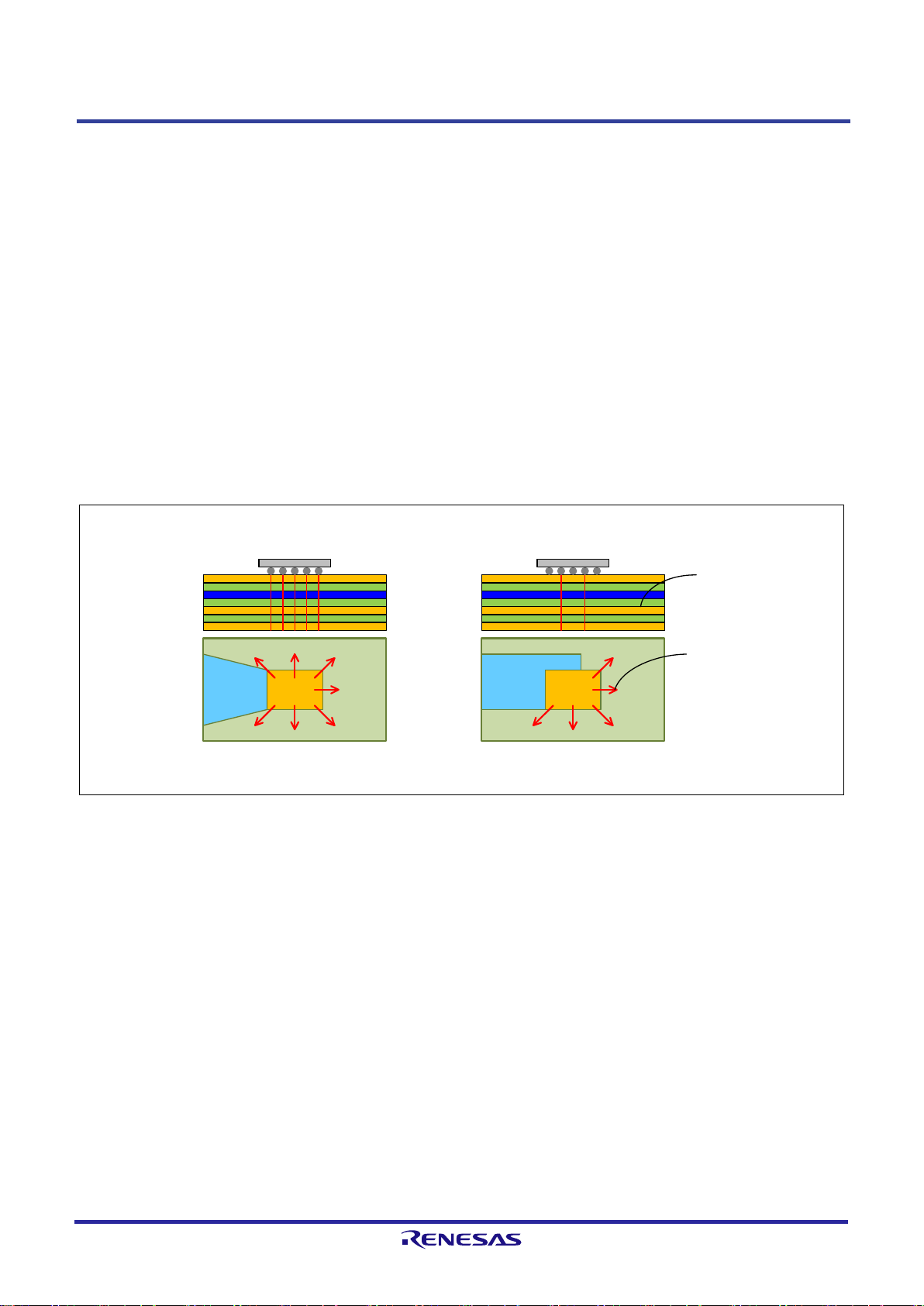
R-IN32M3 Series: Board design edition 25. Thermal Design <R>
GNDGND
L1
L2 (GND)
L3
L4
○: Recommended example
L1
L2 (GND)
L3
L4
△: Exa mple of less effecti ve heat dissipation
AG ND
AG ND
Therm al vi as
Paths for heat
dissipation
GND pattern for securing the maximum
area for heat dissipation paths
GND pattern w here pat hs for heat
diss ipat ion are bloc k ed by AGND
25.2.1 Measures for Heat Release in Designing the Board
(1) Thermal Vias
Placing as many vias to the power supply and GND areas as possible below the center of the package increases the
number of paths for the flow of heat in the z direction. We recommend placing one via for each power supply and GND
ball.
(2) Power Supply and GND Planes
Secure as large an area as is possible for the power supply and GND planes of the board. This enables the broad diffusion
of heat through vias in the direct ion of the surface plane. Dividing paths for heat dissipation from plane to plane
decreases the effectiveness of heat dissipation. Therefore, place the GND pattern in s uch a way that the paths are divided
as little as is possible. We recommend L2 for the GND layer.
R18UZ0021EJ0400 Page 59 of 64
Dec. 28, 2018
Page 71

R-IN32M3 Series: Board design edition 25. Thermal Design <R>
L1
L2 (GND)
L3
L4
L1
L2 (GND)
L3
L4
Thermal vias
L5
L6
The heat of the GND layer diffu ses t hrough L1 to L6.
.
For example, placing a regulator with
has
the effect of significantly reducing its heat dissipation.
(3) Increase the Number of Board Layers, and Bring the GND Pattern out to the Surface Layer
Increasing the number of Cu wiring layers in the printed circuit board expands the area for hear release. Where possible,
place areas of the GND pattern on the surface layer and connect them to the main GND pattern via thermal vias. This
further improves heat dissipation. The board should have at least four layers, and we recommend six.
(4) Consider Other Factors of Plac e ment that will Affect Heat Flows and Take the Appropriate
Action
Placing heat-ge nerating components close to this device affec ts its heat efficiency, so do not place heat-generating
components in its vicinity.
Caution
high power consumption in the vici nit y of this device
(5) Residual Copper Ratio of Cu Layers
Increasing the residual copper ratio in all layers of the board layers increases the breadth of the paths for heat transfer.
(6) Cu Thickness
Designing al l Cu layers of the board to be thick increases the volume of paths for heat dissipation. Since thinner Cu
layers reduce the effectiveness of heat dissipation, care is required on this point. We recommend that the power supply
and GND layers be at least 35-um thick.
R18UZ0021EJ0400 Page 60 of 64
Dec. 28, 2018
Page 72

R-IN32M3 Series: Board design edition 25. Thermal Design <R>
25.2.2 Heat Dissipation from the Periphery (Including the Casing)
(1) Incorporating a Heat Sink
Incorporating a heat s ink increases the area for heat dissipation, making heat dissipation from the surface of the device
more efficient.
(2) Heat Conduction to the Casing
Placing heat dissipating gel on the surface of the device and connecting this to the metal surface of the casing increases
the efficie ncy of heat dissipatio n from the surface of the device.
(3) Placing a Fan in the Casing
Including a fan improves thermal conductivity through convection, which decreases the ambient temperature.
(4) Obtaining a Chimney Effect
Since heat tends to be released in the z direction, p la c ing the board vertically leads to heat convection from the surface of
the device, improving the thermal conductivity rate there.
(5) Enlarging Ventilation Holes
Larger ventilation holes accelerate the heat exchange between the air within the casing and that outside, lowering the
temperature in the vicinity of the device.
(6) Thermal Insulation by Shielding Plates
If there is a particular source of much heat within the casing, thermal insulation by using shielding plate s is effective.
Shielding t he device from the effects of such heat sources reduces the effect of the heat on the device.
R18UZ0021EJ0400 Page 61 of 64
Dec. 28, 2018
Page 73

R-IN32M3 Series: Board design edition 25. Thermal Design <R>
R-IN32M3
Output mod e enabled
Steady-state
current
R-IN32M3
Output m ode dis abled
Open-circuit
(floating)
Thro ugh-typ e
current
VDD33 (3.3 V)
VDD33 (3.3 V)
VDD33 (3.3 V)
VDD33 (3.3 V)
25.3 Points for Caution
This section describes points of incorrect design that ma y lea d to abnormal heating.
25.3.1 Internal Regulator
The 1.5V regulator incorporated in the R-IN32M3-EC requires an external smoothing circuit. This smoothing circ uit not
operating stably (e.g. oscillating around 1.5 V) reduces the efficiency of the regulator and may lead to the sup ply of a
current above the rated value. Inappropriate equivalent series resistances (ESRs) for capacitors are the most li kely source
of such problems. Thus, when usi ng components other than those recommended, use a capacitor with an ESR in the
range from about 75 mΩ to 300 mΩ and check that the outp ut voltage is stable. When using tantalum capacitors is not
possible, a ceramic capacitor and a combination of a 100-mΩ resistor and ceramic capacitor can be used for C2 and C1,
respectively.
25.3.2 Handling of Unused Pins
If an unused pin is clamped to the GND or power supply on the board, the corresponding pin must have the input
attribute as a fixed setting. If it is set as an output, and the level of the point where it is clamped is o pposite that of the pin,
a large steady-state current will continuously flow through the output buffer.
On the other hand, if an unused pi n is open-circuit on the board, the corresponding pin can have either a fixed output
attribute or an input attribute with enabling of pull-up or pull-down resistors. Setting a pin as an input wit ho ut ena bling a
pull-up or pull-down resistor may lead to the pin being i n a floating state and the flow of a through-type current.
Since the above factors lead to unnecessary heating, be sure to check the settings made by the software.
R18UZ0021EJ0400 Page 62 of 64
Dec. 28, 2018
Page 74

R-IN32M3 Series: Board design edition 25. Thermal Design <R>
R18UZ0021EJ0400 Page 63 of 64
Dec. 28, 2018
Page 75

R-IN32M3 Series: Board design edition 26. Countermeasure for Noise <R>
26. Countermeasure for Noise <R>
This section describes a countermeasure for noise in circuits that include an R-IN32M3.
26.1 Stopping Clock Output
If the BUSCLK pin is not in use, outp ut on the pin from an R-IN32M3 can be stopped. See section 2.2.2, Clock Control
Registers (CLK GTD0, CLKGTD1) in the R-IN32M3 Series User’s Manual: Peripheral Modules regarding control of the
GCBCLK bit in the CLKGTD0 register, which enables or disables output from the BUSCLK pin.
R18UZ0021EJ0400 Page 64 of 64
Dec. 28, 2018
Page 76

R-IN32M3 Series: Board design edition Revision History
REVISION HISTORY
R-IN32M3 Series User’s Manual (Board design edition)
Description
Page
Summary
1.00
Jul 26, 2013
-
First edition issued
10,12
Add the TEST pin processing
22
Add “ 9. Notes of CC-Link IE FIeld user (only R-IN32M3-CL)”
11
Add a description of 6. GPIO port pins
20
Add a description of 8.GMII pins
23
Modify a description of 10. Notes of CC-Link IE Field use
24
Add a description of “11. External MPU/memory interface pins”
33
Add a description of “12. Serial Flash ROM memory connection pins”
34
Add a description of “13. Asynchronous Serial Interface J(UARTJ) connection pins”
35
Add a description of “14. I2C connection pins”
36
Add a description of “15. EtherCAT EEPROM I2C connection pins”
37
Add a description of “17. CAN pins”
38
Add a description of “17.JTAG/trace pins”
24
Modify the mode description of the case of MEMCSEL=High and HIFSYNC=Low.
Add the description of Note4-6 of “Fig 11.1” and “Fig 11.2”
Add the description of Note4-6 of “Fig 11.3”, “Fig 11.4”
mode”
2
Add a notes of “2.1 Power-on-off sequence”
1-9
Modify Eglish expression about capter 1-4
used”
25-29
Fig.11.1-11.6 Modify signal name BUSCLK to HBUSCLK
40
Add a description in “17.JTAG/trace pins”
22, 23
Add Fig. 9.1 in 9.CC-Link pins
Synchronous SRAM type transmission mode
3.00
Feb. 28, 2017
1
“1.1 Definition of Pin Handling and Symbols in This Manual” was newly added.
Caution on a resonator was modified.
Pin handling and the GND description in Figure 4.1 were modified.
Rev. Date
1.01 Dec 02, 2013
2.00 Dec 26, 2013
2.01 Feb 07, 2014
25,26 Delete HBCYSTZ pin connection of “Fig 11.1” and “Fig 11.2”
Modifiy the width of data bus of “Fig 11.2”
27,28 Delete HBCYSTZ pin connection of “Fig 11.3” and “Fig 11.4”
Modifiy the width of data bus of “Fig 11.4”
Modifiy the width of address bus of “Fig 11.4”
29, 30 Separete and add the description about “synchronous SRAM type transmission
2.02 May 30, 2014
2.03 Sep 30, 2014 11 Modify part name of inductor VLC5028T to VLCF5028T in “5.1Built-in regulator
used”
Modify ESR value of condenser 300 ohm to 300 mohm in “5.1Built-in regulator
2.04 Dec 25, 2014
29, 30 Modify Fig.11.5, 11.6 to add HBCYSTZ connection, modify Adress bus number,
and delete HHPGCSZ connection. And modify Note2, 4, 5 description in 11.1.3
7 3.3 Oscillation Circuit Configuration Example
Pin handling and the GND description in Figure 3.2 were modified.
8 4.1 Recommended Configuration of Filter
R18UZ0021EJ0400 C - 1
Dec. 28, 2018
Page 77

R-IN32M3 Series: Board design edition Revision History
Description
Page
Summary
on the capacitor substitution method was adde d.
Table 5.1 was added to complement the list of the recommended parts.
Pin handling and the GND description in Figure 5.3 were modified.
The reference in separate user’s manuals, modified
section title.
pins were modified.
Notes were moved to outside of the figure frame.
Notes were moved to outside of the figure frame.
Note was added to R1 to R6 in Table 7.1.
moved to outside of the figure frame.
figure frame.
The description of the number for Ethernet ports was mod ified.
CC-Link clock pins was modified. Note 3 was added.
the CC-Link IE field wad added.
position for the HBUSCLK pin and Note was modified.
The position for the HBUSCLK pin in Figure 11.3 and Figure 11.4 was modified.
position for the HBUSCLK pin and Note was modified.
Rev. Date
3.00 Feb. 28, 2017 10 5.1 Built-in Regulator Used
Pin handling and the GND description in Figure 5.1 were modified. The description
11 5.1 Built-in Regulator Used
12 5.2 Built-in Regulator Unused
13 6. GPIO Port Pins
14 7. Ethernet PHY Pins (R-IN32M3-EC Only)
The description that this section was for the R-IN32M3-EC only was added to the
7.1 Ethernet PHY Power Supply Pins
Pin names of Rx/Tx analog power supply pins and the description of power supply
15 7.2 100Base-TX Pins
Pin handling and the GND description in Figure 7.2 were modified. Remark and
16 7.2 100Base-TX Pins
Pin handling and the GND description in Figure 7.3 were modified. Remark and
7.2 100Base-TX Pins
19 7.3 100Base-FX Pins (Optical Fiber)
Pin handling and the GND description in Figure 7.7 were modified. Remark was
20 8. GMII Pins (R-IN32M3-CL Only)
Pin handling in Figure 8.1 was modified. Remark was moved to outside of the
21 8.2 Circuit Design around GMII
23 9. CC-Link Pins
Pin handling and the GND description in Figure 9.1 were modified. The name for
25 11. External MCU/Memory Interface Pins
As the mode setting pin, the ADMUXMODE pin was added. Note when accessing
27 11.1.1 Asynchronous SRAM Interface Mode
The description of pin handling in Figure 11.1 and Figure 11.2 was modified. The
29 11.1.2 Synchronous SRAM Interface Mode
30 11.1.3 Synchronous SRAM-Type Transfer Mode
The description of pin handling in Figure 11.5 and Figure 11.6 was modified. The
R18UZ0021EJ0400 C - 2
Dec. 28, 2018
Page 78

R-IN32M3 Series: Board design edition Revision History
Description
Page
Summary
As it was not needed, the description on the MEMIFSEL pin was deleted.
Remarks in Figure 11.7 and Figure 11.8 were moved to outside of the figure frame.
frame. The description of Note was modified.
The description of Note in Figure 11.13 and Figure 11.14 was modified.
The name of port pin was added to the pin name in Figure 12.1.
The section title was modified. The name of port pin was modified in Figure 13.1.
port pin.
multiplexing port was added to the EtherCAT pin.
added. Remark was moved to outside of the figure frame.
modified. Pin handling and the GND description were modified.
the GND description were modified.
modified. Pin handling and the GND description were modified.
The website was modified.
modified.
The product name and the marking information of the R-IN32M3-CL were modified.
61
The names of R-IN pins were modified in the connection example.
Newly added
Rev. Date
3.00 Feb. 28, 2017 31 11.2 External Memory Interface
32 11.2.1.1 Connection Example with SRAM
35 11.2.2.1 Connection Example with SRAM
Remarks in Figure 11.11 and Figure 11.12 were moved to outside of the figure
36 11.2.2.2 Connection Example with Paged ROM
37 12. Serial Flash ROM Connection Pins
38 13. Asynchronous Serial Interface J Connection Pins
39 14. I2C Connection Pins
Pin handling in Figure 14.1 was modified. The name of I2C pin was added to the
40 15. EtherCAT EEPROM I2C Connection Pins (R-IN32M3-EC Only)
The description of pin handling in Figure 15.1 was modified. The name of the
41 16. CAN Pins
The name of port pin was modified in Figure 16.1. The name of the CAN pin was
42 17. JTAG/Trace Pins
The connection of the ICE connector to the nRESET pin in Figure 17.1 was
43 17. JTAG/Trace Pins
The connection of the ICE connector to the nRESET pin in Figure 17.2 was
modified. The description on the wiring limitation was modified. Pin handling and
44 17. JTAG/Trace Pins
The connection of the ICE connector to the nRESET pin in Figure 17.3 was
51 22. IBIS Information
52 23.1 R-IN32M3-EC
The product name and the marking information of the R-IN32M3-EC were
23.2 R-IN32M3-CL
53 to
4.00 Dec. 28, 2018 37 Figure 12.1 Connection Example with Serial Flash ROM
42 17 CSIH Pins
R18UZ0021EJ0400 C - 3
Dec. 28, 2018
“24. Guide to Thermal Design” was newly added.
Page 79

R-IN32M3 Series: Board design edition Revision History
Description
Page
Summary
FB, P0_SD_N, and P1_SD_N were added in the R-IN32M3-EC.
The description on notes on using BSDL was added.
Section title was modified.
Newly added
—
Error corrected, description modified, and contents and expressions adjusted
Rev. Date
4.00 Dec. 28, 2018 50 Table 22.1 L ist of BSCAN Non-Supported Pins
51 22.6 Notes on Using BSDL
54 25. Thermal Design
64 26. Countermeasure for Noise
R18UZ0021EJ0400 C - 4
Dec. 28, 2018
Page 80

R-IN32M3 Series: Board design edition Revision History
[Memo]
R18UZ0021EJ0400 C - 5
Dec. 28, 2018
Page 81

Published by: Renesas Electronics Corporation
R-IN32M3 Series User’s Manual: Board design edition
Publication Date: Rev.1.00 Jul. 26, 2013
Rev.4.00 Dec. 28, 2018
Page 82

R18UZ0021EJ0400
R-IN32M3 Series User’s Manual
Board design edition
Page 83

http://www.renesas.com
SALES OFFICES
© 2018 Renesas Electronics Corporation. All rights reserved.
Colophon 5.0
Refer to "http://www.renesas.com/" for the latest and detailed information.
California Eastern Laboratories, Inc.
4590 Patrick Henry Drive, Santa Clara, California 95054-1817, U.S.A.
Tel: +1-408-919-2500, Fax: +1-408-988-0279
Renesas Electronics Europe Limited
Dukes Meadow, Millboard Road, Bourne End, Buckinghamshire, SL8 5FH, U.K
Tel: +44-1628-651-700, Fax: +44-1628-651-804
Renesas Electronics Europe GmbH
Arcadiastrasse 10, 40472 Düsseldorf, Germany
Tel: +49-211-6503-0, Fax: +49-211-6503-1327
Renesas Electronics (China) Co., Ltd.
Room 1709 Quantum Plaza, No.27 ZhichunLu, Haidian District, Beijing, 100191 P. R. China
Tel: +86-10-8235-1155, Fax: +86-10-8235-7679
Renesas Electronics (Shanghai) Co., Ltd.
Unit 301, Tower A, Central Towers, 555 Langao Road, Putuo District, Shanghai, 200333 P. R. China
Tel: +86-21-2226-0888, Fax: +86-21-2226-0999
Renesas Electronics Hong Kong Limited
Unit 1601-1611, 16/F., Tower 2, Grand Century Place, 193 Prince Edward Road West, Mongkok, Kowloon, Hong Kong
Tel: +852-2265-6688, Fax: +852 2886-9022
Renesas Electronics Taiwan Co., Ltd.
13F, No. 363, Fu Shing North Road, Taipei 10543, Taiwan
Tel: +886-2-8175-9600, Fax: +886 2-8175-9670
Renesas Electronics Singapore Pte. Ltd.
80 Bendemeer Road, Unit #06-02 Hyflux Innovation Centre, Singapore 339949
Tel: +65-6213-0200, Fax: +65-6213-0300
Renesas Electronics Malaysia Sdn.Bhd.
Unit 1207, Block B, Menara Amcorp, Amcorp Trade Centre, No. 18, Jln Persiaran Barat, 46050 Petaling Jaya, Selangor Darul Ehsan, Malaysia
Tel: +60-3-7955-9390, Fax: +60-3-7955-9510
Renesas Electronics India Pvt. Ltd.
No.777C, 100 Feet Road, HAL 2nd Stage, Indiranagar, Bangalore 560 038, India
Tel: +91-80-67208700, Fax: +91-80-67208777
Renesas Electronics Korea Co., Ltd.
17F, KAMCO Yangjae Tower, 262, Gangnam-daero, Gangnam-gu, Seoul, 06265 Korea
Tel: +82-2-558-3737, Fax: +82-2-558-5338
 Loading...