

Page 1

REJ09B0106-0100Z
32
H8SX/1657Group
Hardware Manual
Renesas 32-Bit CISC Microcomputer
H8SX Family / H8SX/1600 Series
H8SX/1657 R5F61657
Rev.1.00
Revision Date: Mar. 18, 2004
Page 2

Rev. 1.00, 03/04, page ii of xl
Page 3

Keep safety first in your circuit designs!
1. Renesas Technology Corp. puts the maximum effort into making semiconductor products better and
more reliable, but there is always the possibility that trouble may occur with them. Trouble with
semiconductors may lead to personal injury, fire or property damage.
Remember to give due consideration to safety when making your circuit designs, with appropriate
measures such as (i) placement of substitutive, auxiliary circuits, (ii) use of nonflammable material or
(iii) prevention against any malfunction or mishap.
Notes regarding these materials
1. These materials are intended as a reference to assist our customers in the selection of the Renesas
Technology Corp. product best suited to the customer's application; they do not convey any license
under any intellectual property rights, or any other rights, belonging to Renesas Technology Corp. or
a third party.
2. Renesas Technology Corp. assumes no responsibility for any damage, or infringement of any thirdparty's rights, originating in the use of any product data, diagrams, charts, programs, algorithms, or
circuit application examples contained in these materials.
3. All information contained in these materials, including product data, diagrams, charts, programs and
algorithms represents information on products at the time of publication of these materials, and are
subject to change by Renesas Technology Corp. without notice due to product improvements or
other reasons. It is therefore recommended that customers contact Renesas Technology Corp. or
an authorized Renesas Technology Corp. product distributor for the latest product information
before purchasing a product listed herein.
The information described here may contain technical inaccuracies or typographical errors.
Renesas Technology Corp. assumes no responsibility for any damage, liability, or other loss rising
from these inaccuracies or errors.
Please also pay attention to information published by Renesas Technology Corp. by various means,
including the Renesas Technology Corp. Semiconductor home page (http://www.renesas.com).
4. When using any or all of the information contained in these materials, including product data,
diagrams, charts, programs, and algorithms, please be sure to evaluate all information as a total
system before making a final decision on the applicability of the information and products. Renesas
Technology Corp. assumes no responsibility for any damage, liability or other loss resulting from the
information contained herein.
5. Renesas Technology Corp. semiconductors are not designed or manufactured for use in a device or
system that is used under circumstances in which human life is potentially at stake. Please contact
Renesas Technology Corp. or an authorized Renesas Technology Corp. product distributor when
considering the use of a product contained herein for any specific purposes, such as apparatus or
systems for transportation, vehicular, medical, aerospace, nuclear, or undersea repeater use.
6. The prior written approval of Renesas Technology Corp. is necessary to reprint or reproduce in
whole or in part these materials.
7. If these products or technologies are subject to the Japanese export control restrictions, they must
be exported under a license from the Japanese government and cannot be imported into a country
other than the approved destination.
Any diversion or reexport contrary to the export control laws and regulations of Japan and/or the
country of destination is prohibited.
8. Please contact Renesas Technology Corp. for further details on these materials or the products
contained therein.
Rev. 1.00, 03/04, page iii of xl
Page 4

General Precautions on Handling of Product
1. Treatment of NC Pins
Note: Do not connect anything to the NC pins.
The NC (not connected) pins are either not connected to any of the internal circuitry or are
used as test pins or to reduce noise. If something is connected to the NC pins, the
operation of the LSI is not guaranteed.
2. Treatment of Unused Input Pins
Note: Fix all unused input pins to high or low level.
Generally, the input pins of CMOS products are high-impedance input pins. If unused pins
are in their open states, intermediate levels are induced by noise in the vicinity, a passthrough current flows internally, and a malfunction may occur.
3. Processing before Initialization
Note: When power is first supplied, the product's state is undefined.
The states of internal circuits are undefined until full power is supplied throughout the
chip and a low level is input on the reset pin. During the period where the states are
undefined, the register settings and the output state of each pin are also undefined. Design
your system so that it does not malfunction because of processing while it is in this
undefined state. For those products which have a reset function, reset the LSI immediately
after the power supply has been turned on.
4. Prohibition of Access to Undefined or Reserved Addresses
Note: Access to undefined or reserved addresses is prohibited.
The undefined or reserved addresses may be used to expand functions, or test registers
may have been be allocated to these addresses. Do not access these registers; the system's
operation is not guaranteed if they are accessed.
Rev. 1.00, 03/04, page iv of xl
Page 5

Configuration of This Manual
This manual comprises the following items:
1. General Precautions on Handling of Product
2. Configuration of This Manual
3. Preface
4. Contents
5. Overview
6. Description of Functional Modules
• CPU and System-Control Modules
• On-Chip Peripheral Modules
The configuration of the functional description of each module differs according to the
module. However, the generic style includes the following items:
i) Feature
ii) Input/Output Pin
iii) Register Description
iv) Operation
v) Usage Note
When designing an application system that includes this LSI, take notes into account. Each section
includes notes in relation to the descriptions given, and usage notes are given, as required, as the
final part of each section.
7. List of Registers
8. Electrical Characteristics
9. Appendix
10. Main Revisions and Additions in this Edition (only for revised versions)
The list of revisions is a summary of points that have been revised or added to earlier versions.
This does not include all of the revised contents. For details, see the actual locations in this
manual.
11. Index
Rev. 1.00, 03/04, page v of xl
Page 6

Preface
The H8SX/1657 is a single-chip microcomputer made up of the high-speed internal 32-bit H8SX
CPU as its core, and the peripheral functions required to configure a system. The H8SX CPU is
upward compatible with the H8/300, H8/300H, and H8S CPUs.
Target Users: This manual was written for users who will be using the H8SX/1657 in the design
of application systems. Target users are expected to understand the fundamentals
of electrical circuits, logical circuits, and microcomputers.
Objective: This manual was written to explain the hardware functions and electrical
characteristics of the H8SX/1657 to the target users.
Refer to the H8SX Programming Manual for a detailed description of the
instruction set.
Notes on reading this manual:
• In order to understand the overall functions of the chip
Read the manual according to the contents. This manual can be roughly categorized into parts
on the CPU, system control functions, peripheral functions and electrical characteristics.
• In order to understand the details of the CPU's functions
Read the H8SX Programming Manual.
• In order to understand the details of a register when its name is known
Read the index that is the final part of the manual to find the page number of the entry on the
register. The addresses, bits, and initial values of the registers are summarized in section 21,
List of Registers.
Examples: Register name: The following notation is used for cases when the same or a
similar function, e.g. 16-bit timer pulse unit or serial
communication interface, is implemented on more than one
channel:
XXX_N (XXX is the register name and N is the channel
number)
Bit order: The MSB is on the left and the LSB is on the right.
Number notation: Binary is B′xxxx, hexadecimal is H'xxxx, decimal is xxxx.
Signal notation: An overbar is added to a low-active signal: xxxx
Related Manuals: The latest versions of all related manuals are available from our web site.
Please ensure you have the latest versions of all documents you require.
http://www.renesas.com/eng/
Rev. 1.00, 03/04, page vi of xl
Page 7

H8SX/1657 Group manuals:
Document Title Document No.
H8SX/1657 Group Hardware Manual This manual
H8/SX Programming Manual REJ09B0102
Rev. 1.00, 03/04, page vii of xl
Page 8

Rev. 1.00, 03/04, page viii of xl
Page 9

Contents
Section 1 Overview............................................................................................1
1.1 Features............................................................................................................................. 1
1.2 Block Diagram.................................................................................................................. 2
1.3 Pin Assignments................................................................................................................3
1.3.1 Pin Assignments ..................................................................................................3
1.3.2 Pin Configuration in Each Operating Mode.........................................................4
1.3.3 Pin Functions ....................................................................................................... 8
Section 2 CPU....................................................................................................17
2.1 Features............................................................................................................................. 17
2.2 CPU Operating Modes...................................................................................................... 19
2.2.1 Normal Mode....................................................................................................... 19
2.2.2 Middle Mode ....................................................................................................... 21
2.2.3 Advanced Mode................................................................................................... 22
2.2.4 Maximum Mode .................................................................................................. 23
2.3 Instruction Fetch ...............................................................................................................25
2.4 Address Space...................................................................................................................25
2.5 Registers............................................................................................................................26
2.5.1 General Registers................................................................................................. 27
2.5.2 Program Counter (PC) .........................................................................................28
2.5.3 Condition-Code Register (CCR).......................................................................... 29
2.5.4 Extended Control Register (EXR) .......................................................................30
2.5.5 Vector Base Register (VBR)................................................................................ 31
2.5.6 Short Address Base Register (SBR).....................................................................31
2.5.7 Multiply-Accumulate Register (MAC)................................................................ 31
2.5.8 Initial Values of CPU Registers........................................................................... 31
2.6 Data Formats..................................................................................................................... 32
2.6.1 General Register Data Formats............................................................................ 32
2.6.2 Memory Data Formats......................................................................................... 33
2.7 Instruction Set................................................................................................................... 34
2.7.1 Instructions and Addressing Modes..................................................................... 36
2.7.2 Table of Instructions Classified by Function ....................................................... 40
2.7.3 Basic Instruction Formats .................................................................................... 50
2.8 Addressing Modes and Effective Address Calculation..................................................... 51
2.8.1 Register DirectRn ............................................................................................ 51
2.8.2 Register Indirect@ERn.................................................................................... 52
2.8.3 Register Indirect with Displacement @(d:2, ERn), @(d:16, ERn),
or @(d:32, ERn)...................................................................................................52
Rev. 1.00, 03/04, page ix of xl
Page 10

2.8.4 Index Register Indirect with Displacement@(d:16,RnL.B),
@(d:32,RnL.B), @(d:16,Rn.W), @(d:32,Rn.W), @(d:16,ERn.L), or
@(d:32,ERn.L) .................................................................................................... 52
2.8.5 Register Indirect with Post-Increment, Pre-Decrement, Pre-Increment,
or Post-Decrement@ERn+, @−ERn, @+ERn, or @ERn− ............................. 52
2.8.6 Absolute Address@aa:8, @aa:16, @aa:24, or @aa:32....................................53
2.8.7 Immediate#xx .................................................................................................. 54
2.8.8 Program-Counter Relative@(d:8, PC) or @(d:16, PC): .................................. 54
2.8.9 Program-Counter Relative with Index Register@(RnL.B, PC),
@(Rn.W, PC), or @(ERn.L, PC)......................................................................... 55
2.8.10 Memory Indirect@@aa:8 ................................................................................ 55
2.8.11 Extended Memory Indirect@@vec:7 .............................................................. 56
2.8.12 Effective Address Calculation .............................................................................56
2.8.13 MOVA Instruction............................................................................................... 58
2.9 Processing States...............................................................................................................59
Section 3 MCU Operating Modes .....................................................................61
3.1 Operating Mode Selection ................................................................................................ 61
3.2 Register Descriptions........................................................................................................ 62
3.2.1 Mode Control Register (MDCR) ......................................................................... 62
3.2.2 System Control Register (SYSCR)...................................................................... 63
3.3 Operating Mode Descriptions........................................................................................... 66
3.3.1 Mode 1................................................................................................................. 66
3.3.2 Mode 2................................................................................................................. 66
3.3.3 Mode 4................................................................................................................. 66
3.3.4 Mode 5................................................................................................................. 67
3.3.5 Mode 6................................................................................................................. 67
3.3.6 Mode 7................................................................................................................. 67
3.3.7 Pin Functions ....................................................................................................... 68
3.4 Address Map.....................................................................................................................69
3.4.1 Address Map........................................................................................................ 69
Section 4 Exception Handling........................................................................... 71
4.1 Exception Handling Types and Priority............................................................................ 71
4.2 Exception Sources and Exception Handling Vector Table............................................... 72
4.3 Reset ................................................................................................................................. 74
4.3.1 Reset Exception Handling ................................................................................... 74
4.3.2 Interrupts after Reset............................................................................................ 74
4.3.3 On-Chip Peripheral Functions after Reset Release.............................................. 74
4.4 Traces................................................................................................................................ 77
4.5 Address Error.................................................................................................................... 78
4.5.1 Address Error Source........................................................................................... 78
4.5.2 Address Error Exception Handling...................................................................... 79
Rev. 1.00, 03/04, page x of xl
Page 11

4.6 Interrupts........................................................................................................................... 80
4.6.1 Interrupt Sources.................................................................................................. 80
4.6.2 Interrupt Exception Handling ..............................................................................80
4.7 Instruction Exception Handling ........................................................................................81
4.7.1 Trap Instruction.................................................................................................... 81
4.7.2 Exception Handling by Illegal Instruction ........................................................... 82
4.8 Stack Status after Exception Handling..............................................................................83
4.9 Usage Note........................................................................................................................ 84
Section 5 Interrupt Controller ............................................................................85
5.1 Features............................................................................................................................. 85
5.2 Input/Output Pins.............................................................................................................. 87
5.3 Register Descriptions........................................................................................................ 87
5.3.1 Interrupt Control Register (INTCR) ....................................................................88
5.3.2 CPU Priority Control Register (CPUPCR) .......................................................... 89
5.3.3 Interrupt Priority Registers A to C, E to I, K, and L
(IPRA to IPRC, IPRE to IPRI, IPRK, and IPRL) ................................................90
5.3.4 IRQ Enable Register (IER) ..................................................................................92
5.3.5 IRQ Sense Control Registers H and L (ISCRH, ISCRL)..................................... 94
5.3.6 IRQ Status Register (ISR).................................................................................... 98
5.3.7 Software Standby Release IRQ Enable Register (SSIER)................................... 99
5.4 Interrupt Sources...............................................................................................................100
5.4.1 External Interrupts ...............................................................................................100
5.4.2 Internal Interrupts ................................................................................................101
5.5 Interrupt Exception Handling Vector Table...................................................................... 102
5.6 Interrupt Control Modes and Interrupt Operation............................................................. 106
5.6.1 Interrupt Control Mode 0..................................................................................... 106
5.6.2 Interrupt Control Mode 2..................................................................................... 108
5.6.3 Interrupt Exception Handling Sequence .............................................................. 110
5.6.4 Interrupt Response Times ....................................................................................111
5.6.5 DTC and DMAC Activation by Interrupt ............................................................ 112
5.7 CPU Priority Control Function Over DTC and DMAC.................................................... 115
5.8 Usage Notes...................................................................................................................... 118
5.8.1 Conflict between Interrupt Generation and Disabling ......................................... 118
5.8.2 Instructions that Disable Interrupts...................................................................... 119
5.8.3 Times when Interrupts are Disabled .................................................................... 119
5.8.4 Interrupts during Execution of EEPMOV Instruction.......................................... 119
5.8.5 Interrupts during Execution of MOVMD and MOVSD Instructions...................119
5.8.6 Interrupts of Peripheral Modules .........................................................................120
Section 6 Bus Controller (BSC).........................................................................121
6.1 Features............................................................................................................................. 121
6.2 Register Descriptions........................................................................................................ 124
Rev. 1.00, 03/04, page xi of xl
Page 12

6.2.1 Bus Width Control Register (ABWCR) .............................................................. 125
6.2.2 Access State Control Register (ASTCR) ............................................................. 126
6.2.3 Wait Control Registers A and B (WTCRA, WTCRB) ........................................ 127
6.2.4 Read Strobe Timing Control Register (RDNCR) ................................................ 132
6.2.5 CS Assertion Period Control Registers (CSACR) ............................................... 133
6.2.6 Idle Control Register (IDLCR)............................................................................ 135
6.2.7 Bus Control Register 1 (BCR1) ........................................................................... 137
6.2.8 Bus Control Register 2 (BCR2) ........................................................................... 139
6.2.9 Endian Control Register (ENDIANCR) ..............................................................140
6.2.10 SRAM Mode Control Register (SRAMCR) ........................................................ 141
6.2.11 Burst ROM Interface Control Register (BROMCR) ........................................... 142
6.2.12 Address/Data Multiplexed I/O Control Register (MPXCR) ................................ 144
6.3 Bus Configuration............................................................................................................. 145
6.4 Multi-Clock Function and Number of Access Cycles ...................................................... 146
6.5 External Bus...................................................................................................................... 149
6.5.1 Input/Output Pins................................................................................................. 149
6.5.2 Area Division....................................................................................................... 152
6.5.3 Chip Select Signals.............................................................................................. 153
6.5.4 External Bus Interface .........................................................................................154
6.5.5 Area and External Bus Interface.......................................................................... 158
6.5.6 Endian and Data Alignment................................................................................. 162
6.6 Basic Bus Interface........................................................................................................... 165
6.6.1 Data Bus .............................................................................................................. 165
6.6.2 I/O Pins Used for Basic Bus Interface ................................................................. 165
6.6.3 Basic Timing........................................................................................................166
6.6.4 Wait Control ........................................................................................................ 170
6.6.5 Read Strobe (RD) Timing.................................................................................... 172
6.6.6 Extension of Chip Select (CS) Assertion Period ................................................. 173
6.6.7 DACK Signal Output Timing .............................................................................. 175
6.7 Byte Control SRAM Interface .......................................................................................... 176
6.7.1 Byte Control SRAM Space Setting...................................................................... 176
6.7.2 Data Bus .............................................................................................................. 176
6.7.3 I/O Pins Used for Byte Control SRAM Interface ................................................ 176
6.7.4 Basic Timing........................................................................................................177
6.7.5 Wait Control ........................................................................................................ 180
6.7.6 Read Strobe (RD) ................................................................................................ 182
6.7.7 Extension of Chip Select (CS) Assertion Period ................................................. 182
6.7.8 DACK Signal Output Timing .............................................................................. 182
6.8 Burst ROM Interface ........................................................................................................184
6.8.1 Burst ROM Space Setting.................................................................................... 184
6.8.2 Data Bus .............................................................................................................. 184
6.8.3 I/O Pins Used for Burst ROM Interface............................................................... 185
6.8.4 Basic Timing........................................................................................................186
Rev. 1.00, 03/04, page xii of xl
Page 13

6.8.5 Wait Control ........................................................................................................188
6.8.6 Read Strobe (RD) Timing.................................................................................... 188
6.8.7 Extension of Chip Select (CS) Assertion Period.................................................. 188
6.9 Address/Data Multiplexed I/O Interface........................................................................... 189
6.9.1 Address/Data Multiplexed I/O Space Setting ...................................................... 189
6.9.2 Address/Data Multiplex....................................................................................... 189
6.9.3 Data Bus...............................................................................................................189
6.9.4 I/O Pins Used for Address/Data Multiplexed I/O Interface................................. 190
6.9.5 Basic Timing........................................................................................................191
6.9.6 Address Cycle Control......................................................................................... 193
6.9.7 Wait Control ........................................................................................................194
6.9.8 Read Strobe (RD) Timing................................................................................... 194
6.9.9 Extension of Chip Select (CS) Assertion Period.................................................. 196
6.9.10 DACK Signal Output Timing .............................................................................. 198
6.10 Idle Cycle.......................................................................................................................... 199
6.10.1 Operation ............................................................................................................. 199
6.10.2 Pin States in Idle Cycle ........................................................................................ 208
6.11 Bus Release....................................................................................................................... 209
6.11.1 Operation ............................................................................................................. 209
6.11.2 Pin States in External Bus Released State............................................................ 210
6.11.3 Transition Timing ................................................................................................211
6.12 Internal Bus....................................................................................................................... 212
6.12.1 Access to Internal Address Space ........................................................................ 212
6.13 Write Data Buffer Function .............................................................................................. 213
6.13.1 Write Data Buffer Function for External Data Bus.............................................. 213
6.13.2 Write Data Buffer Function for Peripheral Modules ...........................................214
6.14 Bus Arbitration.................................................................................................................. 215
6.14.1 Operation ............................................................................................................. 215
6.14.2 Bus Transfer Timing............................................................................................ 216
6.15 Bus Controller Operation in Reset .................................................................................... 217
6.16 Usage Notes ......................................................................................................................218
Section 7 DMA Controller (DMAC) .................................................................219
7.1 Features............................................................................................................................. 219
7.2 Input/Output Pins.............................................................................................................. 221
7.3 Register Descriptions........................................................................................................ 222
7.3.1 DMA Source Address Register (DSAR) .............................................................223
7.3.2 DMA Destination Address Register (DDAR)...................................................... 224
7.3.3 DMA Offset Register (DOFR)............................................................................. 225
7.3.4 DMA Transfer Count Register (DTCR) ..............................................................226
7.3.5 DMA Block Size Register (DBSR) .....................................................................227
7.3.6 DMA Mode Control Register (DMDR)............................................................... 228
7.3.7 DMA Address Control Register (DACR)............................................................ 235
Rev. 1.00, 03/04, page xiii of xl
Page 14

7.3.8 DMA Module Request Select Register (DMRSR) .............................................. 241
7.4 Transfer Modes................................................................................................................. 241
7.5 Operations......................................................................................................................... 242
7.5.1 Address Modes ....................................................................................................242
7.5.2 Transfer Modes.................................................................................................... 245
7.5.3 Activation Sources............................................................................................... 250
7.5.4 Bus Access Modes............................................................................................... 252
7.5.5 Extended Repeat Area Function .......................................................................... 254
7.5.6 Address Update Function using Offset ................................................................ 256
7.5.7 Register during DMA Transfer............................................................................ 260
7.5.8 Priority of Channels............................................................................................. 265
7.5.9 DMA Basic Bus Cycle......................................................................................... 266
7.5.10 Bus Cycles in Dual Address Mode ...................................................................... 267
7.5.11 Bus Cycles in Single Address Mode.................................................................... 276
7.6 DMA Transfer End........................................................................................................... 281
7.7 Relationship among DMAC and Other Bus Masters ........................................................ 283
7.7.1 CPU Priority Control Function Over DMAC ...................................................... 283
7.7.2 Bus Arbitration among DMAC and Other Bus Masters ...................................... 284
7.8 Interrupt Sources...............................................................................................................285
7.9 Notes on Usage................................................................................................................. 288
Section 8 Data Transfer Controller (DTC)........................................................ 289
8.1 Features............................................................................................................................. 289
8.2 Register Descriptions........................................................................................................ 291
8.2.1 DTC Mode Register A (MRA) ............................................................................ 292
8.2.2 DTC Mode Register B (MRB)............................................................................. 293
8.2.3 DTC Source Address Register (SAR).................................................................. 294
8.2.4 DTC Destination Address Register (DAR).......................................................... 294
8.2.5 DTC Transfer Count Register A (CRA) .............................................................. 295
8.2.6 DTC Transfer Count Register B (CRB)............................................................... 295
8.2.7 DTC Enable Registers A to H (DTCERA to DTCERE)...................................... 296
8.2.8 DTC Control Register (DTCCR)......................................................................... 297
8.2.9 DTC Vector Base Register (DTCVBR)............................................................... 298
8.3 Activation Sources............................................................................................................ 299
8.4 Location of Transfer Information and DTC Vector Table................................................ 299
8.5 Operation .......................................................................................................................... 303
8.5.1 Bus Cycle Division .............................................................................................. 305
8.5.2 Transfer Information Read Skip Function ........................................................... 307
8.5.3 Transfer Information Writeback Skip Function................................................... 308
8.5.4 Normal Transfer Mode ........................................................................................ 308
8.5.5 Repeat Transfer Mode .........................................................................................309
8.5.6 Block Transfer Mode........................................................................................... 311
8.5.7 Chain Transfer ..................................................................................................... 312
Rev. 1.00, 03/04, page xiv of xl
Page 15

8.5.8 Operation Timing................................................................................................. 313
8.5.9 Number of DTC Execution Cycles ...................................................................... 315
8.5.10 DTC Bus Release Timing .................................................................................... 316
8.5.11 DTC Priority Level Control to the CPU ..............................................................316
8.6 DTC Activation by Interrupt............................................................................................. 317
8.7 Examples of Use of the DTC............................................................................................ 318
8.7.1 Normal Transfer Mode ........................................................................................318
8.7.2 Chain Transfer ..................................................................................................... 318
8.7.3 Chain Transfer when Counter = 0........................................................................ 319
8.8 Interrupt Sources...............................................................................................................321
8.9 Usage Notes...................................................................................................................... 321
8.9.1 Module Stop Mode Setting .................................................................................. 321
8.9.2 On-Chip RAM ..................................................................................................... 321
8.9.3 DMAC Transfer End Interrupt............................................................................. 321
8.9.4 DTCE Bit Setting................................................................................................. 321
8.9.5 Chain Transfer ..................................................................................................... 322
8.9.6 Transfer Information Start Address, Source Address,
and Destination Address ......................................................................................322
8.9.7 Transfer Information Modification ...................................................................... 322
8.9.8 Endian Format...................................................................................................... 322
Section 9 I/O Ports.............................................................................................323
9.1 Register Descriptions........................................................................................................ 329
9.1.1 Data Direction Register (PnDDR) (n = 1 to 3, 6, A, B, D to F, H, and I)............ 330
9.1.2 Data Register (PnDR) (n = 1 to 3, 6, A, B, D to F, H, and I)............................... 330
9.1.3 Port Register (PORTn) (n = 1 to 3, 5, 6, A, B, D to F, H, and I) .........................331
9.1.4 Input Buffer Control Register
(PnICR) (n = 1 to 3, 5, 6, A, B, D to F, H, and I) ................................................331
9.1.5 Pull-Up MOS Control Register (PnPCR) (n = D to F, H, and I)..........................332
9.1.6 Open-Drain Control Register (PnODR) (n = 2 and F)......................................... 333
9.2 Output Buffer Control....................................................................................................... 334
9.2.1 Port 1....................................................................................................................334
9.2.2 Port 2....................................................................................................................337
9.2.3 Port 3....................................................................................................................340
9.2.4 Port 5....................................................................................................................343
9.2.5 Port 6....................................................................................................................343
9.2.6 Port A................................................................................................................... 345
9.2.7 Port B................................................................................................................... 349
9.2.8 Port D................................................................................................................... 351
9.2.9 Port E................................................................................................................... 352
9.2.10 Port F ................................................................................................................... 352
9.2.11 Port H................................................................................................................... 356
9.2.12 Port I ....................................................................................................................356
Rev. 1.00, 03/04, page xv of xl
Page 16

9.3 Port Function Controller................................................................................................... 362
9.3.1 Port Function Control Register 0 (PFCR0).......................................................... 362
9.3.2 Port Function Control Register 1 (PFCR1).......................................................... 363
9.3.3 Port Function Control Register 2 (PFCR2).......................................................... 364
9.3.4 Port Function Control Register 4 (PFCR4).......................................................... 365
9.3.5 Port Function Control Register 6 (PFCR6).......................................................... 367
9.3.6 Port Function Control Register 7 (PFCR7).......................................................... 368
9.3.7 Port Function Control Register 9 (PFCR9).......................................................... 369
9.3.8 Port Function Control Register B (PFCRB) ........................................................370
9.3.9 Port Function Control Register C (PFCRC) ........................................................371
9.4 Usage Notes...................................................................................................................... 373
9.4.1 Notes on Input Buffer Control Register (ICR) Setting ........................................373
9.4.2 Notes on Port Function Control Register (PFCR) Settings.................................. 373
Section 10 16-Bit Timer Pulse Unit (TPU) .......................................................375
10.1 Features............................................................................................................................. 375
10.2 Input/Output Pins.............................................................................................................. 379
10.3 Register Descriptions........................................................................................................ 380
10.3.1 Timer Control Register (TCR)............................................................................. 382
10.3.2 Timer Mode Register (TMDR)............................................................................ 387
10.3.3 Timer I/O Control Register (TIOR)..................................................................... 388
10.3.4 Timer Interrupt Enable Register (TIER).............................................................. 406
10.3.5 Timer Status Register (TSR)................................................................................ 408
10.3.6 Timer Counter (TCNT)........................................................................................ 411
10.3.7 Timer General Register (TGR) ............................................................................ 411
10.3.8 Timer Start Register (TSTR) ............................................................................... 412
10.3.9 Timer Synchronous Register (TSYR).................................................................. 413
10.4 Operation ..........................................................................................................................414
10.4.1 Basic Functions.................................................................................................... 414
10.4.2 Synchronous Operation........................................................................................ 420
10.4.3 Buffer Operation .................................................................................................. 422
10.4.4 Cascaded Operation ............................................................................................. 426
10.4.5 PWM Modes ........................................................................................................ 428
10.4.6 Phase Counting Mode.......................................................................................... 433
10.5 Interrupt Sources...............................................................................................................439
10.6 DTC Activation................................................................................................................. 441
10.7 DMAC Activation............................................................................................................. 441
10.8 A/D Converter Activation................................................................................................. 441
10.9 Operation Timing.............................................................................................................. 442
10.9.1 Input/Output Timing ............................................................................................ 442
10.9.2 Interrupt Signal Timing ....................................................................................... 446
10.10 Usage Notes ......................................................................................................................449
10.10.1 Module Stop Mode Setting.................................................................................. 449
Rev. 1.00, 03/04, page xvi of xl
Page 17

10.10.2 Input Clock Restrictions ......................................................................................449
10.10.3 Caution on Cycle Setting ..................................................................................... 450
10.10.4 Conflict between TCNT Write and Clear Operations.......................................... 450
10.10.5 Conflict between TCNT Write and Increment Operations ..................................451
10.10.6 Conflict between TGR Write and Compare Match..............................................451
10.10.7 Conflict between Buffer Register Write and Compare Match ............................. 452
10.10.8 Conflict between TGR Read and Input Capture .................................................. 452
10.10.9 Conflict between TGR Write and Input Capture .................................................453
10.10.10 Conflict between Buffer Register Write and Input Capture............................... 454
10.10.11 Conflict between Overflow/Underflow and Counter Clearing ..........................455
10.10.12 Conflict between TCNT Write and Overflow/Underflow .................................455
10.10.13 Multiplexing of I/O Pins.................................................................................... 456
10.10.14 Interrupts and Module Stop Mode ..................................................................... 456
Section 11 Programmable Pulse Generator (PPG) ............................................457
11.1 Features............................................................................................................................. 457
11.2 Input/Output Pins.............................................................................................................. 458
11.3 Register Descriptions........................................................................................................ 459
11.3.1 Next Data Enable Registers H, L (NDERH, NDERL) ........................................ 459
11.3.2 Output Data Registers H, L (PODRH, PODRL).................................................. 461
11.3.3 Next Data Registers H, L (NDRH, NDRL) ......................................................... 462
11.3.4 PPG Output Control Register (PCR) ................................................................... 465
11.3.5 PPG Output Mode Register (PMR) ..................................................................... 466
11.4 Operation ..........................................................................................................................468
11.4.1 Output Timing...................................................................................................... 468
11.4.2 Sample Setup Procedure for Normal Pulse Output.............................................. 469
11.4.3 Example of Normal Pulse Output (Example of 5-Phase Pulse Output) ............... 470
11.4.4 Non-Overlapping Pulse Output............................................................................ 471
11.4.5 Sample Setup Procedure for Non-Overlapping Pulse Output .............................. 473
11.4.6 Example of Non-Overlapping Pulse Output
(Example of 4-Phase Complementary Non-Overlapping Pulse Output) .............474
11.4.7 Inverted Pulse Output ..........................................................................................476
11.4.8 Pulse Output Triggered by Input Capture ............................................................ 477
11.5 Usage Notes ......................................................................................................................478
11.5.1 Module Stop Mode Setting .................................................................................. 478
11.5.2 Operation of Pulse Output Pins............................................................................ 478
Section 12 8-Bit Timers (TMR).........................................................................479
12.1 Features............................................................................................................................. 479
12.2 Input/Output Pins.............................................................................................................. 482
12.3 Register Descriptions........................................................................................................ 483
12.3.1 Timer Counter (TCNT)........................................................................................ 484
12.3.2 Time Constant Register A (TCORA)................................................................... 484
Rev. 1.00, 03/04, page xvii of xl
Page 18

12.3.3 Time Constant Register B (TCORB) ................................................................... 485
12.3.4 Timer Control Register (TCR)............................................................................ 485
12.3.5 Timer Counter Control Register (TCCR) ........................................................... 487
12.3.6 Timer Control/Status Register (TCSR)................................................................ 489
12.4 Operation ..........................................................................................................................493
12.4.1 Pulse Output ........................................................................................................ 493
12.4.2 Reset Input ........................................................................................................... 494
12.5 Operation Timing.............................................................................................................. 495
12.5.1 TCNT Count Timing ........................................................................................... 495
12.5.2 Timing of CMFA and CMFB Setting at Compare Match ................................... 496
12.5.3 Timing of Timer Output at Compare Match........................................................ 496
12.5.4 Timing of Counter Clear by Compare Match ...................................................... 497
12.5.5 Timing of TCNT External Reset.......................................................................... 497
12.5.6 Timing of Overflow Flag (OVF) Setting .............................................................498
12.6 Operation with Cascaded Connection............................................................................... 499
12.6.1 16-Bit Counter Mode ........................................................................................... 499
12.6.2 Compare Match Count Mode .............................................................................. 499
12.7 Interrupt Sources...............................................................................................................500
12.7.1 Interrupt Sources and DTC Activation ................................................................ 500
12.7.2 A/D Converter Activation.................................................................................... 500
12.8 Usage Notes ...................................................................................................................... 501
12.8.1 Notes on Setting Cycle ........................................................................................ 501
12.8.2 Conflict between TCNT Write and Clear ............................................................501
12.8.3 Conflict between TCNT Write and Increment..................................................... 502
12.8.4 Conflict between TCOR Write and Compare Match........................................... 503
12.8.5 Conflict between Compare Matches A and B...................................................... 503
12.8.6 Switching of Internal Clocks and TCNT Operation ............................................ 504
12.8.7 Mode Setting with Cascaded Connection ............................................................505
12.8.8 Module Stop Mode Setting .................................................................................. 505
12.8.9 Interrupts in Module Stop Mode.......................................................................... 506
Section 13 Watchdog Timer (WDT) .................................................................507
13.1 Features............................................................................................................................. 507
13.2 Input/Output Pin ............................................................................................................... 508
13.3 Register Descriptions........................................................................................................ 508
13.3.1 Timer Counter (TCNT)........................................................................................ 508
13.3.2 Timer Control/Status Register (TCSR)................................................................ 508
13.3.3 Reset Control/Status Register (RSTCSR)............................................................ 510
13.4 Operation ..........................................................................................................................511
13.4.1 Watchdog Timer Mode ........................................................................................ 511
13.4.2 Interval Timer Mode............................................................................................ 512
13.5 Interrupt Source ................................................................................................................513
13.6 Usage Notes ...................................................................................................................... 513
Rev. 1.00, 03/04, page xviii of xl
Page 19

13.6.1 Notes on Register Access..................................................................................... 513
13.6.2 Conflict between Timer Counter (TCNT) Write and Increment.......................... 514
13.6.3 Changing Values of Bits CKS2 to CKS0............................................................. 515
13.6.4 Switching between Watchdog Timer Mode and Interval Timer Mode................ 515
13.6.5 Internal Reset in Watchdog Timer Mode............................................................. 515
13.6.6 System Reset by WDTOVF Signal...................................................................... 515
13.6.7 Transition to Watchdog Timer Mode or Software Standby Mode....................... 516
Section 14 Serial Communication Interface (SCI) ............................................517
14.1 Features............................................................................................................................. 517
14.2 Input/Output Pins.............................................................................................................. 519
14.3 Register Descriptions........................................................................................................ 519
14.3.1 Receive Shift Register (RSR) .............................................................................. 521
14.3.2 Receive Data Register (RDR) .............................................................................. 521
14.3.3 Transmit Data Register (TDR)............................................................................. 521
14.3.4 Transmit Shift Register (TSR) ............................................................................. 521
14.3.5 Serial Mode Register (SMR) ............................................................................... 522
14.3.6 Serial Control Register (SCR) ............................................................................. 525
14.3.7 Serial Status Register (SSR) ................................................................................529
14.3.8 Smart Card Mode Register (SCMR) .................................................................... 536
14.3.9 Bit Rate Register (BRR) ...................................................................................... 537
14.3.10 Serial Extended Mode Register (SEMR)............................................................. 544
14.4 Operation in Asynchronous Mode ....................................................................................546
14.4.1 Data Transfer Format........................................................................................... 547
14.4.2 Receive Data Sampling Timing
and Reception Margin in Asynchronous Mode ...................................................548
14.4.3 Clock.................................................................................................................... 549
14.4.4 SCI Initialization (Asynchronous Mode) .............................................................550
14.4.5 Serial Data Transmission (Asynchronous Mode) ................................................ 551
14.4.6 Serial Data Reception (Asynchronous Mode)...................................................... 553
14.5 Multiprocessor Communication Function......................................................................... 557
14.5.1 Multiprocessor Serial Data Transmission ............................................................558
14.5.2 Multiprocessor Serial Data Reception ................................................................. 559
14.6 Operation in Clocked Synchronous Mode........................................................................ 562
14.6.1 Clock.................................................................................................................... 562
14.6.2 SCI Initialization (Clocked Synchronous Mode) ................................................. 563
14.6.3 Serial Data Transmission (Clocked Synchronous Mode) ....................................564
14.6.4 Serial Data Reception (Clocked Synchronous Mode).......................................... 566
14.6.5 Simultaneous Serial Data Transmission and Reception
(Clocked Synchronous Mode) .............................................................................567
14.7 Operation in Smart Card Interface Mode.......................................................................... 569
14.7.1 Sample Connection ..............................................................................................569
14.7.2 Data Format (Except in Block Transfer Mode) ...................................................570
Rev. 1.00, 03/04, page xix of xl
Page 20

14.7.3 Block Transfer Mode ........................................................................................... 571
14.7.4 Receive Data Sampling Timing and Reception Margin ...................................... 572
14.7.5 Initialization ......................................................................................................... 573
14.7.6 Data Transmission (Except in Block Transfer Mode) ......................................... 574
14.7.7 Serial Data Reception (Except in Block Transfer Mode) .................................... 577
14.7.8 Clock Output Control........................................................................................... 578
14.8 Interrupt Sources...............................................................................................................580
14.8.1 Interrupts in Normal Serial Communication Interface Mode .............................. 580
14.8.2 Interrupts in Smart Card Interface Mode ............................................................. 581
14.9 Usage Notes ...................................................................................................................... 582
14.9.1 Module Stop Mode Setting .................................................................................. 582
14.9.2 Break Detection and Processing .......................................................................... 582
14.9.3 Mark State and Break Detection .......................................................................... 582
14.9.4 Receive Error Flags and Transmit Operations
(Clocked Synchronous Mode Only) .................................................................... 582
14.9.5 Relation between Writing to TDR and TDRE Flag ............................................. 582
14.9.6 Restrictions on Using DMAC or DTC................................................................. 583
14.9.7 SCI Operations during Mode Transitions ............................................................ 583
Section 15 A/D Converter ................................................................................. 587
15.1 Features............................................................................................................................. 587
15.2 Input/Output Pins.............................................................................................................. 589
15.3 Register Descriptions........................................................................................................ 589
15.3.1 A/D Data Registers A to H (ADDRA to ADDRH) ............................................. 590
15.3.2 A/D Control/Status Register (ADCSR) ...............................................................591
15.3.3 A/D Control Register (ADCR) ............................................................................ 593
15.4 Operation ..........................................................................................................................594
15.4.1 Single Mode......................................................................................................... 594
15.4.2 Scan Mode ...........................................................................................................595
15.4.3 Input Sampling and A/D Conversion Time ......................................................... 597
15.4.4 External Trigger Input Timing............................................................................. 598
15.5 Interrupt Source ................................................................................................................599
15.6 A/D Conversion Accuracy Definitions............................................................................. 599
15.7 Usage Notes ...................................................................................................................... 601
15.7.1 Module Stop Mode Setting .................................................................................. 601
15.7.2 Permissible Signal Source Impedance ................................................................. 601
15.7.3 Influences on Absolute Accuracy ........................................................................ 601
15.7.4 Setting Range of Analog Power Supply and Other Pins...................................... 602
15.7.5 Notes on Board Design ........................................................................................ 602
15.7.6 Notes on Noise Countermeasures ........................................................................ 602
15.7.7 A/D Input Hold Function in Software Standby Mode .........................................603
Rev. 1.00, 03/04, page xx of xl
Page 21

Section 16 D/A Converter..................................................................................605
16.1 Features............................................................................................................................. 605
16.2 Input/Output Pins.............................................................................................................. 606
16.3 Register Descriptions........................................................................................................ 606
16.3.1 D/A Data Registers 0 and 1 (DADR0 and DADR1)............................................ 606
16.3.2 D/A Control Register 01 (DACR01) ................................................................... 607
16.4 Operation ..........................................................................................................................609
16.5 Usage Notes ......................................................................................................................610
16.5.1 Module Stop Mode Setting .................................................................................. 610
16.5.2 D/A Output Hold Function in Software Standby Mode.......................................610
Section 17 RAM ................................................................................................611
Section 18 Flash Memory (0.18-µm F-ZTAT Version) ....................................613
18.1 Features............................................................................................................................. 613
18.2 Mode Transition Diagram................................................................................................. 615
18.3 Memory MAT Configuration............................................................................................ 617
18.4 Block Structure .................................................................................................................618
18.5 Programming/Erasing Interface ........................................................................................ 619
18.6 Input/Output Pins.............................................................................................................. 621
18.7 Register Descriptions........................................................................................................ 621
18.7.1 Programming/Erasing Interface Registers ...........................................................622
18.7.2 Programming/Erasing Interface Parameters ........................................................629
18.7.3 RAM Emulation Register (RAMER)................................................................... 641
18.8 On-Board Programming Mode .........................................................................................642
18.8.1 Boot Mode ...........................................................................................................642
18.8.2 User Program Mode............................................................................................. 646
18.8.3 User Boot Mode................................................................................................... 656
18.8.4 On-Chip Program and Storable Area for Program Data ...................................... 660
18.9 Protection.......................................................................................................................... 665
18.9.1 Hardware Protection ............................................................................................665
18.9.2 Software Protection.............................................................................................. 666
18.9.3 Error Protection.................................................................................................... 666
18.10 Flash Memory Emulation Using RAM ............................................................................. 668
18.11 Switching between User MAT and User Boot MAT ........................................................ 671
18.12 Programmer Mode ............................................................................................................672
18.13 Standard Serial Communication Interface Specifications for Boot Mode ........................672
18.14 Usage Notes ......................................................................................................................699
Section 19 Clock Pulse Generator .....................................................................701
19.1 Register Description.......................................................................................................... 702
19.1.1 System Clock Control Register (SCKCR) ........................................................... 702
Rev. 1.00, 03/04, page xxi of xl
Page 22

19.2 Oscillator........................................................................................................................... 704
19.2.1 Connecting Crystal Resonator ............................................................................. 704
19.2.2 External Clock Input ............................................................................................ 705
19.3 PLL Circuit ....................................................................................................................... 706
19.4 Frequency Divider ............................................................................................................706
19.5 Usage Notes ...................................................................................................................... 706
19.5.1 Notes on Clock Pulse Generator .......................................................................... 706
19.5.2 Notes on Resonator.............................................................................................. 707
19.5.3 Notes on Board Design ........................................................................................ 708
Section 20 Power-Down Modes........................................................................ 709
20.1 Features............................................................................................................................. 709
20.2 Register Descriptions........................................................................................................ 712
20.2.1 Standby Control Register (SBYCR) .................................................................... 712
20.2.2 Module Stop Control Registers A and B (MSTPCRA and MSTPCRB) ............. 714
20.2.3 Module Stop Control Register C (MSTPCRC).................................................... 717
20.3 Multi-Clock Function ....................................................................................................... 718
20.4 Sleep Mode ....................................................................................................................... 719
20.4.1 Transition to Sleep Mode..................................................................................... 719
20.4.2 Clearing Sleep Mode ........................................................................................... 719
20.5 Software Standby Mode.................................................................................................... 720
20.5.1 Transition to Software Standby Mode ................................................................. 720
20.5.2 Clearing Software Standby Mode ........................................................................ 720
20.5.3 Setting Oscillation Settling Time after Clearing Software Standby Mode ..........721
20.5.4 Software Standby Mode Application Example.................................................... 723
20.6 Hardware Standby Mode .................................................................................................. 724
20.6.1 Transition to Hardware Standby Mode................................................................ 724
20.6.2 Clearing Hardware Standby Mode....................................................................... 724
20.6.3 Hardware Standby Mode Timing......................................................................... 724
20.6.4 Timing Sequence at Power-On ............................................................................ 725
20.7 Module Stop Mode ...........................................................................................................726
20.7.1 Module Stop Mode .............................................................................................. 726
20.7.2 All-Module-Clock-Stop Mode............................................................................. 726
20.8 Bφ Clock Output Control.................................................................................................. 727
20.9 Usage Notes ...................................................................................................................... 728
20.9.1 I/O Port Status...................................................................................................... 728
20.9.2 Current Consumption during Oscillation Settling Standby Period ......................728
20.9.3 Module Stop Mode of DMAC or DTC................................................................ 728
20.9.4 On-Chip Peripheral Module Interrupts ................................................................ 728
20.9.5 Writing to MSTPCRA, MSTPCRB, and MSTPCRC .......................................... 728
Rev. 1.00, 03/04, page xxii of xl
Page 23

Section 21 List of Registers ...............................................................................729
21.1 Register Addresses (Address Order)................................................................................. 730
21.2 Register Bits...................................................................................................................... 740
21.3 Register States in Each Operating Mode ..........................................................................753
Section 22 Electrical Characteristics .................................................................763
22.1 Absolute Maximum Ratings ............................................................................................. 763
22.2 DC Characteristics ............................................................................................................ 764
22.3 AC Characteristics ............................................................................................................ 767
22.3.1 Clock Timing ....................................................................................................... 768
22.3.2 Control Signal Timing .........................................................................................770
22.3.3 Bus Timing .......................................................................................................... 771
22.3.4 DMAC Timing..................................................................................................... 786
22.3.5 Timing of On-Chip Peripheral Modules ..............................................................789
22.4 A/D Conversion Characteristics........................................................................................ 792
22.5 D/A Conversion Characteristics........................................................................................ 793
22.6 Flash Memory Characteristics ..........................................................................................794
Appendix .........................................................................................................795
A. Port States in Each Pin State............................................................................................. 795
B. Product Lineup..................................................................................................................800
C. Package Dimensions .........................................................................................................801
Index .........................................................................................................805
Rev. 1.00, 03/04, page xxiii of xl
Page 24

Rev. 1.00, 03/04, page xxiv of xl
Page 25

Figures
Section 1 Overview
Figure 1.1 Block Diagram ..............................................................................................................2
Figure 1.2 Pin Assignments............................................................................................................ 3
Section 2 CPU
Figure 2.1 CPU Operating Modes ................................................................................................19
Figure 2.2 Exception Vector Table (Normal Mode)..................................................................... 20
Figure 2.3 Stack Structure (Normal Mode) ..................................................................................20
Figure 2.4 Exception Vector Table (Middle and Advanced Modes)............................................ 22
Figure 2.5 Stack Structure (Middle and Advanced Modes).......................................................... 23
Figure 2.6 Exception Vector Table (Maximum Modes)............................................................... 24
Figure 2.7 Stack Structure (Maximum Mode).............................................................................. 24
Figure 2.8 Memory Map............................................................................................................... 25
Figure 2.9 CPU Registers ............................................................................................................. 26
Figure 2.10 Usage of General Registers....................................................................................... 27
Figure 2.11 Stack.......................................................................................................................... 28
Figure 2.12 General Register Data Formats .................................................................................32
Figure 2.13 Memory Data Formats...............................................................................................33
Figure 2.14 Instruction Formats.................................................................................................... 50
Figure 2.15 Branch Address Specification in Memory Indirect Mode......................................... 55
Figure 2.16 State Transitions........................................................................................................ 60
Section 3 MCU Operating Modes
Figure 3.1 Address Map (1).......................................................................................................... 69
Figure 3.2 Address Map (2).......................................................................................................... 70
Section 4 Exception Handling
Figure 4.1 Reset Sequence (On-chip ROM Enabled Advanced Mode)........................................75
Figure 4.2 Reset Sequence
(16-Bit External Access in On-chip ROM Disabled Advanced Mode) ......................76
Figure 4.3 Stack Status after Exception Handling........................................................................ 83
Figure 4.4 Operation when SP Value Is Odd................................................................................ 84
Section 5 Interrupt Controller
Figure 5.1 Block Diagram of Interrupt Controller........................................................................ 86
Figure 5.2 Block Diagram of Interrupts IRQn............................................................................ 101
Figure 5.3 Flowchart of Procedure Up to Interrupt Acceptance in Interrupt Control Mode 0... 107
Figure 5.4 Flowchart of Procedure Up to Interrupt Acceptance in Interrupt Control Mode 2... 109
Figure 5.5 Interrupt Exception Handling.................................................................................... 110
Figure 5.6 Block Diagram of DTC, DMAC, and Interrupt Controller ....................................... 113
Figure 5.7 Conflict between Interrupt Generation and Disabling............................................... 118
Rev. 1.00, 03/04, page xxv of xl
Page 26

Section 6 Bus Controller (BSC)
Figure 6.1 Block Diagram of Bus Controller..............................................................................123
Figure 6.2 Read Strobe Negation Timing (Example of 3-State Access Space).......................... 133
Figure 6.3 CS and Address Assertion Period Extension
(Example of Basic Bus Interface, 3-State Access Space, and RDNn = 0)................. 135
Figure 6.4 Internal Bus Configuration........................................................................................ 145
Figure 6.5 System Clock: External Bus Clock = 4:1, External 2-State Access .......................... 147
Figure 6.6 System Clock: External Bus Clock = 2:1, External 3-State Access .......................... 148
Figure 6.7 Address Space Area Division.................................................................................... 152
Figure 6.8 CSn Signal Output Timing (n = 0 to 7)..................................................................... 153
Figure 6.9 Timing When CS Signal is Output to the Same Pin.................................................. 154
Figure 6.10 Access Sizes and Data Alignment Control for 8-Bit Access Space
(Big Endian) ...........................................................................................................162
Figure 6.11 Access Sizes and Data Alignment Control for 8-Bit Access Space
(Little Endian)......................................................................................................... 163
Figure 6.12 Access Sizes and Data Alignment Control for 16-Bit Access Space
(Big Endian) ...........................................................................................................164
Figure 6.13 Access Sizes and Data Alignment Control for 16-Bit Access Space
(Little Endian).......................................................................................................... 164
Figure 6.14 16-Bit 2-State Access Space Bus Timing (Byte Access for Even Address)........... 166
Figure 6.15 16-Bit 2-State Access Space Bus Timing (Byte Access for Odd Address)............ 167
Figure 6.16 16-Bit 2-State Access Space Bus Timing (Word Access for Even Address)......... 168
Figure 6.17 16-Bit 3-State Access Space Bus Timing (Byte Access for Even Address)........... 169
Figure 6.18 16-Bit 3-State Access Space Bus Timing (Word Access for Odd Address) ..........170
Figure 6.19 16-Bit 3-State Access Space Bus Timing (Word Access for Even Address)......... 171
Figure 6.20 Example of Wait Cycle Insertion Timing................................................................ 173
Figure 6.21 Example of Read Strobe Timing ............................................................................. 174
Figure 6.22 Example of Timing when Chip Select Assertion Period is Extended ..................... 176
Figure 6.23 DACK Signal Output Timing.................................................................................. 177
Figure 6.24 16-Bit 2-State Access Space Bus Timing................................................................ 180
Figure 6.25 16-Bit 3-State Access Space Bus Timing................................................................ 181
Figure 6.26 Example of Wait Cycle Insertion Timing................................................................ 183
Figure 6.27 DACK Signal Output Timing.................................................................................. 185
Figure 6.28 Example of Burst ROM Access Timing (ASTn = 1, Two Burst Cycles)................ 188
Figure 6.29 Example of Burst ROM Access Timing (ASTn = 0, One Burst Cycle) .................. 189
Figure 6.30 8-Bit Access Space Access Timing (ABWHn = 1, ABWLn = 1) ........................... 193
Figure 6.31 16-Bit Access Space Access Timing (ABWHn = 0, ABWLn = 1)......................... 194
Figure 6.32 Access Timing of 3 Address Cycles (ADDEX = 1)................................................ 195
Figure 6.33 Read Strobe Timing ................................................................................................197
Figure 6.34 Chip Select (CS) Assertion Period Extension Timing in Data Cycle...................... 198
Figure 6.35 Consecutive Read Accesses to Same Area
(Address/Data Multiplexed I/O Space).................................................................... 199
Figure 6.36 DACK Signal Output Timing.................................................................................. 200
Rev. 1.00, 03/04, page xxvi of xl
Page 27

Figure 6.37 Example of Idle Cycle Operation (Consecutive Reads in Different Areas) ............203
Figure 6.38 Example of Idle Cycle Operation (Write after Read).............................................. 204
Figure 6.39 Example of Idle Cycle Operation (Read after Write).............................................. 205
Figure 6.40 Example of Idle Cycle Operation (Write after Single Address Transfer Write)...... 206
Figure 6.41 Idle Cycle Insertion Example.................................................................................. 207
Figure 6.42 Relationship between Chip Select (CS) and Read (RD)..........................................208
Figure 6.43 Bus Released State Transition Timing ....................................................................213
Figure 6.44 Example of Timing when Write Data Buffer Function is Used .............................. 215
Figure 6.45 Example of Timing when Peripheral Module
Write Data Buffer Function is Used ....................................................................... 216
Section 7 DMA Controller (DMAC)
Figure 7.1 Block Diagram of DMAC ......................................................................................... 220
Figure 7.2 Example of Signal Timing in Dual Address Mode....................................................242
Figure 7.3 Operations in Dual Address Mode ............................................................................ 243
Figure 7.4 Data Flow in Single Address Mode........................................................................... 244
Figure 7.5 Example of Signal Timing in Single Address Mode................................................. 244
Figure 7.6 Operations in Single Address Mode.......................................................................... 245
Figure 7.7 Example of Signal Timing in Normal Transfer Mode............................................... 245
Figure 7.8 Operations in Normal Transfer Mode .......................................................................246
Figure 7.9 Operations in Repeat Transfer Mode.........................................................................247
Figure 7.10 Operations in Block Transfer Mode ........................................................................ 248
Figure 7.11 Operation in Single Address Mode in Block Transfer Mode
(Block Area Specified) ............................................................................................248
Figure 7.12 Operation in Dual Address Mode in Block Transfer Mode
(Block Area Not Specified) .................................................................................... 249
Figure 7.13 Example of Timing in Cycle Stealing Mode ........................................................... 252
Figure 7.14 Example of Timing in Burst Mode.......................................................................... 253
Figure 7.15 Example of Extended Repeat Area Operation......................................................... 254
Figure 7.16 Example of Extended Repeat Area Function in Block Transfer Mode ................... 255
Figure 7.17 Address Update Method.......................................................................................... 256
Figure 7.18 Operation of Offset Addition................................................................................... 257
Figure 7.19 XY Conversion Operation Using Offset Addition in Repeat Transfer Mode..........258
Figure 7.20 XY Conversion Flowchart Using Offset Addition in Repeat Transfer Mode .........259
Figure 7.21 Procedure for Changing Register Setting For Channel being Transferred.............. 263
Figure 7.22 Example of Timing for Channel Priority................................................................. 265
Figure 7.23 Example of Bus Timing of DMA Transfer.............................................................. 266
Figure 7.24 Example of Transfer in Normal Transfer Mode by Cycle Stealing......................... 267
Figure 7.25 Example of Transfer in Normal Transfer Mode by Cycle Stealing
(Transfer Source DSAR = Odd Address and Source Address Increment).............. 268
Figure 7.26 Example of Transfer in Normal Transfer Mode by Cycle Stealing (Transfer
Destination DDAR = Odd Address and Destination Address Decrement)............. 268
Figure 7.27 Example of Transfer in Normal Transfer Mode by Burst Access ........................... 269
Rev. 1.00, 03/04, page xxvii of xl
Page 28

Figure 7.28 Example of Transfer in Block Transfer Mode......................................................... 270
Figure 7.29 Example of Transfer in Normal Transfer Mode Activated
by DREQ Falling Edge........................................................................................... 271
Figure 7.30 Example of Transfer in Block Transfer Mode Activated
by DREQ Falling Edge........................................................................................... 272
Figure 7.31 Example of Transfer in Normal Transfer Mode Activated
by DREQ Low Level.............................................................................................. 273
Figure 7.32 Example of Transfer in Block Transfer Mode Activated
by DREQ Low Level............................................................................................... 274
Figure 7.33 Example of Transfer in Normal Transfer Mode Activated
by DREQ Low Level with NRD = 1 ......................................................................275
Figure 7.34 Example of Transfer in Single Address Mode (Byte Read) .................................... 276
Figure 7.35 Example of Transfer in Single Address Mode (Byte Write) .................................... 277
Figure 7.36 Example of Transfer in Single Address Mode Activated
by DREQ Falling Edge........................................................................................... 278
Figure 7.37 Example of Transfer in Single Address Mode Activated by DREQ Low Level..... 279
Figure 7.38 Example of Transfer in Single Address Mode Activated
by DREQ Low Level with NRD = 1 ......................................................................280
Figure 7.39 Interrupt and Interrupt Sources................................................................................ 287
Figure 7.40 Procedure Example of Resuming Transfer by Clearing Interrupt Source ............... 287
Section 8 Data Transfer Controller (DTC)
Figure 8.1 Block Diagram of DTC............................................................................................. 292
Figure 8.2 Transfer Information on Data Area........................................................................... 301
Figure 8.3 Correspondence between DTC Vector Address and Transfer Information............... 302
Figure 8.4 Flowchart of DTC Operation .................................................................................... 306
Figure 8.5 Bus Cycle Division Example .................................................................................... 308
Figure 8.6 Transfer Information Read Skip Timing................................................................... 309
Figure 8.7 Memory Map in Normal Transfer Mode................................................................... 311
Figure 8.8 Memory Map in Repeat Transfer Mode
(When Transfer Source is Specified as Repeat Area)................................................ 312
Figure 8.9 Memory Map in Block Transfer Mode
(When Transfer Destination is Specified as Block Area) .......................................... 313
Figure 8.10 Operation of Chain Transfer.................................................................................... 314
Figure 8.11 DTC Operation Timing (Example of Short Address Mode
in Normal Transfer Mode or Repeat Transfer Mode)............................................. 315
Figure 8.12 DTC Operation Timing (Example of Short Address Mode
in Block Transfer Mode with Block Size of 2)....................................................... 315
Figure 8.13 DTC Operation Timing (Example of Short Address Mode in Chain Transfer) ...... 316
Figure 8.14 DTC Operation Timing (Example of Full Address Mode
in Normal Transfer Mode or Repeat Transfer Mode)............................................. 316
Figure 8.15 DTC with Interrupt Activation................................................................................ 319
Figure 8.16 Chain Transfer when Counter = 0 ........................................................................... 322
Rev. 1.00, 03/04, page xxviii of xl
Page 29

Section 10 16-Bit Timer Pulse Unit (TPU)
Figure 10.1 Block Diagram of TPU............................................................................................ 380
Figure 10.2 Example of Counter Operation Setting Procedure .................................................. 416
Figure 10.3 Free-Running Counter Operation............................................................................ 417
Figure 10.4 Periodic Counter Operation..................................................................................... 418
Figure 10.5 Example of Setting Procedure for Waveform Output by Compare Match.............. 418
Figure 10.6 Example of 0-Output/1-Output Operation............................................................... 419
Figure 10.7 Example of Toggle Output Operation ..................................................................... 419
Figure 10.8 Example of Setting Procedure for Input Capture Operation....................................420
Figure 10.9 Example of Input Capture Operation.......................................................................421
Figure 10.10 Example of Synchronous Operation Setting Procedure ........................................422
Figure 10.11 Example of Synchronous Operation...................................................................... 423
Figure 10.12 Compare Match Buffer Operation......................................................................... 424
Figure 10.13 Input Capture Buffer Operation.............................................................................424
Figure 10.14 Example of Buffer Operation Setting Procedure................................................... 425
Figure 10.15 Example of Buffer Operation (1)...........................................................................426
Figure 10.16 Example of Buffer Operation (2)...........................................................................427
Figure 10.17 Example of Cascaded Operation Setting Procedure.............................................. 428
Figure 10.18 Example of Cascaded Operation (1)...................................................................... 429
Figure 10.19 Example of Cascaded Operation (2)...................................................................... 429
Figure 10.20 Example of PWM Mode Setting Procedure ..........................................................432
Figure 10.21 Example of PWM Mode Operation (1)................................................................. 432
Figure 10.22 Example of PWM Mode Operation (2)................................................................. 433
Figure 10.23 Example of PWM Mode Operation (3)................................................................. 434
Figure 10.24 Example of Phase Counting Mode Setting Procedure........................................... 435
Figure 10.25 Example of Phase Counting Mode 1 Operation .................................................... 436
Figure 10.26 Example of Phase Counting Mode 2 Operation .................................................... 437
Figure 10.27 Example of Phase Counting Mode 3 Operation .................................................... 438
Figure 10.28 Example of Phase Counting Mode 4 Operation .................................................... 439
Figure 10.29 Phase Counting Mode Application Example.........................................................440
Figure 10.30 Count Timing in Internal Clock Operation............................................................444
Figure 10.31 Count Timing in External Clock Operation...........................................................444
Figure 10.32 Output Compare Output Timing ...........................................................................445
Figure 10.33 Input Capture Input Signal Timing........................................................................ 445
Figure 10.34 Counter Clear Timing (Compare Match) .............................................................. 446
Figure 10.35 Counter Clear Timing (Input Capture).................................................................. 446
Figure 10.36 Buffer Operation Timing (Compare Match)..........................................................447
Figure 10.37 Buffer Operation Timing (Input Capture) ............................................................. 447
Figure 10.38 TGI Interrupt Timing (Compare Match) ...............................................................448
Figure 10.39 TGI Interrupt Timing (Input Capture)................................................................... 448
Figure 10.40 TCIV Interrupt Setting Timing.............................................................................. 449
Figure 10.41 TCIU Interrupt Setting Timing.............................................................................. 449
Rev. 1.00, 03/04, page xxix of xl
Page 30

Figure 10.42 Timing for Status Flag Clearing by CPU ..............................................................450
Figure 10.43 Timing for Status Flag Clearing by DTC or DMAC Activation (1)......................450
Figure 10.44 Timing for Status Flag Clearing by DTC or DMAC Activation (2)......................451
Figure 10.45 Phase Difference, Overlap, and Pulse Width in Phase Counting Mode................ 451
Figure 10.46 Conflict between TCNT Write and Clear Operations ........................................... 452
Figure 10.47 Conflict between TCNT Write and Increment Operations.................................... 453
Figure 10.48 Conflict between TGR Write and Compare Match ............................................... 453
Figure 10.49 Conflict between Buffer Register Write and Compare Match .............................. 454
Figure 10.50 Conflict between TGR Read and Input Capture.................................................... 455
Figure 10.51 Conflict between TGR Write and Input Capture................................................... 455
Figure 10.52 Conflict between Buffer Register Write and Input Capture .................................. 456
Figure 10.53 Conflict between Overflow and Counter Clearing................................................ 457
Figure 10.54 Conflict between TCNT Write and Overflow ....................................................... 457
Section 11 Programmable Pulse Generator (PPG)
Figure 11.1 Block Diagram of PPG............................................................................................ 459
Figure 11.2 Schematic Diagram of PPG..................................................................................... 470
Figure 11.3 Timing of Transfer and Output of NDR Contents (Example)................................. 470
Figure 11.4 Setup Procedure for Normal Pulse Output (Example) ............................................ 471
Figure 11.5 Normal Pulse Output Example (5-Phase Pulse Output) .......................................... 472
Figure 11.6 Non-Overlapping Pulse Output ............................................................................... 473
Figure 11.7 Non-Overlapping Operation and NDR Write Timing............................................. 474
Figure 11.8 Setup Procedure for Non-Overlapping Pulse Output (Example).............................475
Figure 11.9 Non-Overlapping Pulse Output Example (4-Phase Complementary) ..................... 476
Figure 11.10 Inverted Pulse Output (Example).......................................................................... 478
Figure 11.11 Pulse Output Triggered by Input Capture (Example)............................................ 479
Section 12 8-Bit Timers (TMR)
Figure 12.1 Block Diagram of 8-Bit Timer Module (Unit 0) ..................................................... 482
Figure 12.2 Block Diagram of 8-Bit Timer Module (Unit 1) ..................................................... 483
Figure 12.3 Example of Pulse Output......................................................................................... 495
Figure 12.4 Example of Reset Input ........................................................................................... 496
Figure 12.5 Count Timing for Internal Clock Input (Falling Edge) ........................................... 497
Figure 12.6 Count Timing for External Clock Input (Both Edges) ............................................497
Figure 12.7 Timing of CMF Setting at Compare Match.............................................................498
Figure 12.8 Timing of Toggled Timer Output at Compare Match A ......................................... 498
Figure 12.9 Timing of Counter Clear by Compare Match.......................................................... 499
Figure 12.10 Timing of Clearance by External Reset (Rising Edge) ......................................... 499
Figure 12.11 Timing of Clearance by External Reset (High Level)........................................... 500
Figure 12.12 Timing of OVF Setting ......................................................................................... 500
Figure 12.13 Conflict between TCNT Write and Clear.............................................................. 503
Figure 12.14 Conflict between TCNT Write and Increment ...................................................... 504
Figure 12.15 Conflict between TCOR Write and Compare Match ............................................ 505
Rev. 1.00, 03/04, page xxx of xl
Page 31

Section 13 Watchdog Timer (WDT)
Figure 13.1 Block Diagram of WDT.......................................................................................... 509
Figure 13.2 Operation in Watchdog Timer Mode.......................................................................514
Figure 13.3 Operation in Interval Timer Mode...........................................................................514
Figure 13.4 Writing to TCNT, TCSR, and RSTCSR.................................................................. 516
Figure 13.5 Conflict between TCNT Write and Increment ........................................................ 516
Figure 13.6 Circuit for System Reset by WDTOVF Signal (Example)...................................... 517
Section 14 Serial Communication Interface (SCI)
Figure 14.1 Block Diagram of SCI............................................................................................. 520
Figure 14.2 Data Format in Asynchronous Communication
(Example with 8-Bit Data, Parity, Two Stop Bits) .................................................548
Figure 14.3 Receive Data Sampling Timing in Asynchronous Mode ........................................550
Figure 14.4 Phase Relation between Output Clock and Transmit Data
(Asynchronous Mode) ............................................................................................ 551
Figure 14.5 Sample SCI Initialization Flowchart .......................................................................552
Figure 14.6 Example of Operation for Transmission in Asynchronous Mode
(Example with 8-Bit Data, Parity, One Stop Bit).................................................... 553
Figure 14.7 Sample Serial Transmission Flowchart ...................................................................554
Figure 14.8 Example of SCI Operation for Reception
(Example with 8-Bit Data, Parity, One Stop Bit).................................................... 555
Figure 14.9 Sample Serial Reception Flowchart (1)................................................................... 557
Figure 14.9 Sample Serial Reception Flowchart (2)................................................................... 558
Figure 14.10 Example of Communication Using Multiprocessor Format
(Transmission of Data H'AA to Receiving Station A).......................................... 559
Figure 14.11 Sample Multiprocessor Serial Transmission Flowchart........................................ 560
Figure 14.12 Example of SCI Operation for Reception
(Example with 8-Bit Data, Multiprocessor Bit, One Stop Bit).............................. 561
Figure 14.13 Sample Multiprocessor Serial Reception Flowchart (1)........................................ 562
Figure 14.13 Sample Multiprocessor Serial Reception Flowchart (2)........................................ 563
Figure 14.14 Data Format in Clocked Synchronous Communication (LSB-First)..................... 564
Figure 14.15 Sample SCI Initialization Flowchart ..................................................................... 565
Figure 14.16 Example of Operation for Transmission in Clocked Synchronous Mode .............566
Figure 14.17 Sample Serial Transmission Flowchart................................................................. 567
Figure 14.18 Example of Operation for Reception in Clocked Synchronous Mode...................568
Figure 14.19 Sample Serial Reception Flowchart ......................................................................569
Figure 14.20 Sample Flowchart of Simultaneous Serial Transmission and Reception ..............570
Figure 14.21 Pin Connection for Smart Card Interface .............................................................. 571
Figure 14.22 Data Formats in Normal Smart Card Interface Mode............................................ 572
Figure 14.23 Direct Convention (SDIR = SINV = O/E = 0) ...................................................... 572
Figure 14.24 Inverse Convention (SDIR = SINV = O/E = 1)..................................................... 573
Figure 14.25 Receive Data Sampling Timing in Smart Card Interface Mode
(When Clock Frequency is 372 Times the Bit Rate) ............................................574
Rev. 1.00, 03/04, page xxxi of xl
Page 32

Figure 14.26 Data Re-Transfer Operation in SCI Transmission Mode ......................................577
Figure 14.27 TEND Flag Set Timing during Transmission........................................................ 577
Figure 14.28 Sample Transmission Flowchart ........................................................................... 578
Figure 14.29 Data Re-Transfer Operation in SCI Reception Mode............................................ 579
Figure 14.30 Sample Reception Flowchart................................................................................. 580
Figure 14.31 Clock Output Fixing Timing ................................................................................. 580
Figure 14.32 Clock Stop and Restart Procedure......................................................................... 581
Figure 14.33 Sample Transmission using DTC in Clocked Synchronous Mode........................ 585
Figure 14.34 Sample Flowchart for Mode Transition during Transmission............................... 586
Figure 14.35 Port Pin States during Mode Transition
(Internal Clock, Asynchronous Transmission) ......................................................587
Figure 14.36 Port Pin States during Mode Transition
(Internal Clock, Clocked Synchronous Transmission) .........................................587
Figure 14.37 Sample Flowchart for Mode Transition during Reception.................................... 588
Section 15 A/D Converter
Figure 15.1 Block Diagram of A/D Converter ........................................................................... 590
Figure 15.2 Example of A/D Converter Operation (Single Mode, Channel 1 Selected)............ 597
Figure 15.3 Example of A/D Conversion
(Scan Mode, Three Channels (AN0 to AN2) Selected).......................................... 598
Figure 15.4 A/D Conversion Timing.......................................................................................... 599
Figure 15.5 External Trigger Input Timing ................................................................................ 600
Figure 15.6 A/D Conversion Accuracy Definitions ...................................................................602
Figure 15.7 A/D Conversion Accuracy Definitions ...................................................................602
Figure 15.8 Example of Analog Input Circuit ............................................................................ 603
Figure 15.9 Example of Analog Input Protection Circuit........................................................... 605
Figure 15.10 Analog Input Pin Equivalent Circuit ..................................................................... 605
Section 16 D/A Converter
Figure 16.1 Block Diagram of D/A Converter ........................................................................... 607
Figure 16.2 Example of D/A Converter Operation..................................................................... 611
Section 18 Flash Memory (0.18-mm F-ZTAT Version)
Figure 18.1 Block Diagram of Flash Memory............................................................................ 616
Figure 18.2 Mode Transition of Flash Memory.......................................................................... 617
Figure 18.3 Memory MAT Configuration.................................................................................. 619
Figure 18.4 Block Structure of User MAT................................................................................. 620
Figure 18.5 Procedure for Creating Procedure Program.............................................................621
Figure 18.6 System Configuration in Boot Mode....................................................................... 644
Figure 18.7 Automatic-Bit-Rate Adjustment Operation............................................................. 645
Figure 18.8 Boot Mode State Transition Diagram...................................................................... 646
Figure 18.9 Example of Erase Block Including Programmed Area............................................647
Figure 18.10 Programming/Erasing Flow ..................................................................................648
Figure 18.11 RAM Map when Programming/Erasing is Executed ............................................ 649
Rev. 1.00, 03/04, page xxxii of xl
Page 33

Figure 18.12 Programming Procedure in User Program Mode ..................................................650
Figure 18.13 Example of Erase Block Including Programmed Area.......................................... 654
Figure 18.14 Erasing Procedure in User Program Mode............................................................ 655
Figure 18.15 Repeating Procedure of Erasing, Programming,
and RAM Emulation in User Program Mode ........................................................657
Figure 18.16 Procedure for Programming User MAT in User Boot Mode ................................659
Figure 18.17 Procedure for Erasing User MAT in User Boot Mode.......................................... 660
Figure 18.18 Transitions to Error Protection State .....................................................................669
Figure 18.19 RAM Emulation Flow........................................................................................... 670
Figure 18.20 Address Map of Overlaid RAM Area....................................................................671
Figure 18.21 Programming Tuned Data ..................................................................................... 672
Figure 18.22 Switching between User MAT and User Boot MAT ............................................673
Figure 18.23 Boot Program States..............................................................................................675
Figure 18.24 Bit-Rate-Adjustment Sequence .............................................................................676
Figure 18.25 Communication Protocol Format .......................................................................... 677
Figure 18.26 New Bit-Rate Selection Sequence......................................................................... 688
Figure 18.27 Programming Sequence......................................................................................... 691
Figure 18.28 Erasure Sequence ..................................................................................................692
Section 19 Clock Pulse Generator
Figure 19.1 Block Diagram of Clock Pulse Generator ...............................................................703
Figure 19.2 Connection of Crystal Resonator (Example)........................................................... 706
Figure 19.3 Crystal Resonator Equivalent Circuit...................................................................... 707
Figure 19.4 External Clock Input (Examples) ............................................................................707
Figure 19.5 Clock Modification Timing..................................................................................... 709
Figure 19.6 Note on Board Design for Oscillation Circuit......................................................... 710
Figure 19.7 Recommended External Circuitry for PLL Circuit .................................................710
Section 20 Power-Down Modes
Figure 20.1 Mode Transitions..................................................................................................... 713
Figure 20.2 Software Standby Mode Application Example ....................................................... 725
Figure 20.3 Hardware Standby Mode Timing ............................................................................726
Figure 20.4 Timing Sequence at Power-On................................................................................ 727
Section 22 Electrical Characteristics
Figure 22.1 Output Load Circuit................................................................................................. 769
Figure 22.2 External Bus Clock Timing..................................................................................... 770
Figure 22.3 Oscillation Settling Timing after Software Standby Mode ..................................... 771
Figure 22.4 Oscillation Settling Timing .....................................................................................771
Figure 22.5 External Input Clock Timing................................................................................... 771
Figure 22.6 Reset Input Timing.................................................................................................. 772
Figure 22.7 Interrupt Input Timing............................................................................................. 773
Figure 22.8 Basic Bus Timing: 2-State Access...........................................................................776
Figure 22.9 Basic Bus Timing: 3-State Access...........................................................................777
Rev. 1.00, 03/04, page xxxiii of xl
Page 34

Figure 22.10 Basic Bus Timing: Three-State Access, One Wait................................................ 778
Figure 22.11 Basic Bus Timing: 2-State Access (CS Assertion Period Extended) .................... 779
Figure 22.12 Basic Bus Timing: 3-State Access (CS Assertion Period Extended) .................... 780
Figure 22.13 Byte Control SRAM: 2-State Read/Write Access................................................. 781
Figure 22.14 Byte Control SRAM: 3-State Read/Write Access................................................. 782
Figure 22.15 Burst ROM Access Timing: 1-State Burst Access................................................ 783
Figure 22.16 Burst ROM Access Timing: 2-State Burst Access................................................ 784
Figure 22.17 Address/Data Multiplexed Access Timing (No Wait) (Basic, 4-State Access)..... 785
Figure 22.18 Address/Data Multiplexed Access Timing (Wait Control)
(Address Cycle Program Wait × 1 + Data Cycle Program Wait × 1
+ Data Cycle Pin Wait × 1).................................................................................. 786
Figure 22.19 External Bus Release Timing................................................................................ 787
Figure 22.20 External Bus Request Output Timing....................................................................787
Figure 22.21 DMAC (DREQ) Input Timing .............................................................................. 788
Figure 22.22 DMAC (TEND) Output Timing............................................................................ 788
Figure 22.23 DMAC Single-Address Transfer Timing: 2-State Access..................................... 789
Figure 22.24 DMAC Single-Address Transfer Timing: 3-State Access..................................... 790
Figure 22.25 I/O Port Input/Output Timing................................................................................ 792
Figure 22.26 TPU Input/Output Timing..................................................................................... 792
Figure 22.27 TPU Clock Input Timing....................................................................................... 792
Figure 22.28 PPG Output Timing............................................................................................... 793
Figure 22.29 8-Bit Timer Output Timing................................................................................... 793
Figure 22.30 8-Bit Timer Reset Input Timing............................................................................ 793
Figure 22.31 8-Bit Timer Clock Input Timing ........................................................................... 793
Figure 22.32 WDT Output Timing............................................................................................. 793
Figure 22.33 SCK Clock Input Timing ......................................................................................793
Figure 22.34 SCI Input/Output Timing: Clocked Synchronous Mode....................................... 794
Figure 22.35 A/D Converter External Trigger Input Timing...................................................... 794
Appendix
Figure C.1 Package Dimensions (TFP-120) ............................................................................... 803
Rev. 1.00, 03/04, page xxxiv of xl
Page 35

Tables
Section 1 Overview
Table 1.1
Table 1.2 Pin Functions ............................................................................................................ 8
Section 2 CPU
Table 2.1
Table 2.2 Combinations of Instructions and Addressing Modes (1)....................................... 36
Table 2.2 Combinations of Instructions and Addressing Modes (2)....................................... 39
Table 2.3 Operation Notation .................................................................................................40
Table 2.4 Data Transfer Instructions.......................................................................................41
Table 2.5 Block Transfer Instructions.....................................................................................42
Table 2.6 Arithmetic Operation Instructions ..........................................................................43
Table 2.7 Logic Operation Instructions ..................................................................................45
Table 2.8 Shift Operation Instructions.................................................................................... 45
Table 2.9 Bit Manipulation Instructions ................................................................................. 46
Table 2.10 Branch Instructions................................................................................................. 48
Table 2.11 System Control Instructions....................................................................................49
Table 2.12 Addressing Modes .................................................................................................. 51
Table 2.13 Absolute Address Access Ranges ........................................................................... 54
Table 2.14 Effective Address Calculation for Transfer and Operation Instructions................. 57
Table 2.15 Effective Address Calculation for Branch Instructions........................................... 58
Pin Configuration in Each Operating Mode..............................................................4
Instruction Classification........................................................................................ 34
Section 3 MCU Operating Modes
Table 3.1
Table 3.2 Settings of Bits MDS3 to MDS0.............................................................................63
Table 3.3 Pin Functions in Each Operating Mode (Advanced Mode) .................................... 68
Section 4 Exception Handling
Table 4.1
Table 4.2 Exception Handling Vector Table...........................................................................72
Table 4.3 Calculation Method of Exception Handling Vector Table Address........................73
Table 4.4 Status of CCR and EXR after Trace Exception Handling.......................................77
Table 4.5 Bus Cycle and Address Error.................................................................................. 78
Table 4.6 Status of CCR and EXR after Address Error Exception Handling ......................... 79
Table 4.7 Interrupt Sources..................................................................................................... 80
Table 4.8 Status of CCR and EXR after Trap Instruction Exception Handling...................... 81
Table 4.9 Status of CCR and EXR after Illegal Instruction Exception Handling ................... 82
Section 5 Interrupt Controller
Table 5.1
Table 5.2 Interrupt Sources, Vector Address Offsets, and Interrupt Priority........................ 102
Table 5.3 Interrupt Control Modes .......................................................................................106
MCU Operating Mode Settings .............................................................................. 61
Exception Types and Priority..................................................................................71
Pin Configuration....................................................................................................87
Rev. 1.00, 03/04, page xxxv of xl
Page 36

Table 5.4 Interrupt Response Times ..................................................................................... 111
Table 5.5 Number of Execution States in Interrupt Handling Routine................................. 112
Table 5.6 Interrupt Source Selection and Clear Control ....................................................... 114
Table 5.7 CPU Priority Control ............................................................................................ 116
Table 5.8 Example of Priority Control Function Setting and Control State ......................... 117
Section 6 Bus Controller (BSC)
Table 6.1
Table 6.2 Pin Configuration.................................................................................................. 149
Table 6.3 Pin Functions in Each Interface............................................................................ 151
Table 6.4 Interface Names and Area Names......................................................................... 154
Table 6.5 Areas Specifiable for Each Interface ....................................................................155
Table 6.6 Number of Access Cycles..................................................................................... 157
Table 6.7 Area 0 External Interface...................................................................................... 158
Table 6.8 Area 1 External Interface...................................................................................... 159
Table 6.9 Area 2 External Interface...................................................................................... 159
Table 6.10 Area 3 External Interface...................................................................................... 159
Table 6.11 Area 4 External Interface...................................................................................... 160
Table 6.12 Area 5 External Interface...................................................................................... 160
Table 6.13 Area 6 External Interface...................................................................................... 161
Table 6.14 Area 7 External Interface...................................................................................... 161
Table 6.15 I/O Pins for Basic Bus Interface ........................................................................... 165
Table 6.16 I/O Pins for Byte Control SRAM Interface ..........................................................179
Table 6.17 I/O Pins Used for Burst ROM Interface................................................................187
Table 6.18 Address/Data Multiplex........................................................................................ 191
Table 6.19 I/O Pins for Address/Data Multiplexed I/O Interface........................................... 192
Table 6.20 Number of Idle Cycle Insertion Selection in Each Area....................................... 202
Table 6.21 Number of Idle Cycle Insertions........................................................................... 202
Table 6.22 Idle Cycles in Mixed Accesses to Normal Space.................................................. 209
Table 6.23 Pin States in Idle Cycle......................................................................................... 210
Table 6.24 Pin States in Bus Released State........................................................................... 212
Table 6.25 Number of Access Cycles for On-Chip Memory Spaces...................................... 214
Table 6.26 Number of Access Cycles for Registers of On-Chip Peripheral Modules ............ 214
Synchronization Clocks and Their Corresponding Functions...............................146
Section 7 DMA Controller (DMAC)
Table 7.1
Table 7.2 Data Access Size, Valid Bits, and Settable Size ................................................... 229
Table 7.3 Settings and Areas of Extended Repeat Area .......................................................242
Table 7.4 Transfer Modes..................................................................................................... 243
Table 7.5 List of On-chip module interrupts to DMAC........................................................253
Table 7.6 Priority among DMAC Channels.......................................................................... 267
Table 7.7 Interrupt Sources and Priority............................................................................... 287
Rev. 1.00, 03/04, page xxxvi of xl
Pin Configuration..................................................................................................223
Page 37

Section 8 Data Transfer Controller (DTC)
Table 8.1
Table 8.2 DTC Transfer Modes ............................................................................................ 305
Table 8.3 Chain Transfer Conditions.................................................................................... 307
Table 8.4 Number of Bus Cycle Divisions and Access Size.................................................307
Table 8.5 Transfer Information Writeback Skip Condition
Table 8.6 Register Function in Normal Transfer Mode........................................................ 310
Table 8.7 Register Function in Repeat Transfer Mode ......................................................... 312
Table 8.8 Register Function in Block Transfer Mode........................................................... 313
Table 8.9 DTC Execution Status........................................................................................... 317
Table 8.10 Number of Cycles Required for Each Execution State......................................... 318
Section 9 I/O Ports
Table 9.1
Table 9.2 Register Configuration in Each Port ..................................................................... 331
Table 9.3 Startup Mode and Initial Value............................................................................. 332
Table 9.4 Input Pull-Up MOS State...................................................................................... 335
Table 9.5 Available Output Signals and Settings in Each Port............................................. 359
Section 10 16-Bit Timer Pulse Unit (TPU)
Table 10.1
Table 10.2 Pin Configuration.................................................................................................. 381
Table 10.3 CCLR2 to CCLR0 (Channels 0 and 3) .................................................................385
Table 10.4 CCLR2 to CCLR0 (Channels 1, 2, 4, and 5) ........................................................385
Table 10.5 Input Clock Edge Selection ..................................................................................386
Table 10.6 TPSC2 to TPSC0 (Channel 0) .............................................................................. 386
Table 10.7 TPSC2 to TPSC0 (Channel 1) .............................................................................. 386
Table 10.8 TPSC2 to TPSC0 (Channel 2) .............................................................................. 387
Table 10.9 TPSC2 to TPSC0 (Channel 3) .............................................................................. 387
Table 10.10 TPSC2 to TPSC0 (Channel 4) ..........................................................................388
Table 10.11 TPSC2 to TPSC0 (Channel 5) ..........................................................................388
Table 10.12 MD3 to MD0 ....................................................................................................390
Table 10.13 TIORH_0 ..........................................................................................................392
Table 10.14 TIORL_0........................................................................................................... 393
Table 10.15 TIOR_1 ............................................................................................................. 394
Table 10.16 TIOR_2 ............................................................................................................. 395
Table 10.17 TIORH_3 ..........................................................................................................396
Table 10.18 TIORL_3........................................................................................................... 397
Table 10.19 TIOR_4 ............................................................................................................. 398
Table 10.20 TIOR_5 ............................................................................................................. 399
Table 10.21 TIORH_0 ..........................................................................................................400
Table 10.22 TIORL_0........................................................................................................... 401
Interrupt Sources, DTC Vector Addresses, and Corresponding DTCEs...............303
and Writeback Skipped Registers .........................................................................310
Port Functions....................................................................................................... 325
TPU Functions ...................................................................................................... 378
Rev. 1.00, 03/04, page xxxvii of xl
Page 38

Table 10.23 TIOR_1............................................................................................................. 402
Table 10.24 TIOR_2............................................................................................................. 403
Table 10.25 TIORH_3 .......................................................................................................... 404
Table 10.26 TIORL_3 .......................................................................................................... 405
Table 10.27 TIOR_4............................................................................................................. 406
Table 10.28 TIOR_5............................................................................................................. 407
Table 10.29 Register Combinations in Buffer Operation ..................................................... 424
Table 10.30 Cascaded Combinations.................................................................................... 428
Table 10.31 PWM Output Registers and Output Pins ..........................................................431
Table 10.32 Clock Input Pins in Phase Counting Mode....................................................... 435
Table 10.33 Up/Down-Count Conditions in Phase Counting Mode 1.................................. 436
Table 10.34 Up/Down-Count Conditions in Phase Counting Mode 2.................................. 437
Table 10.35 Up/Down-Count Conditions in Phase Counting Mode 3.................................. 438
Table 10.36 Up/Down-Count Conditions in Phase Counting Mode 4.................................. 439
Table 10.37 TPU Interrupts .................................................................................................. 441
Section 11 Programmable Pulse Generator (PPG)
Table 11.1
Section 12 8-Bit Timers (TMR)
Table 12.1
Table 12.2 Clock Input to TCNT and Count Condition.......................................................... 490
Table 12.3 8-Bit Timer (TMR_0 or TMR_1) Interrupt Sources............................................. 502
Table 12.4 Timer Output Priorities......................................................................................... 505
Table 12.5 Switching of Internal Clock and TCNT Operation............................................... 506
Pin Configuration.................................................................................................. 460
Pin Configuration.................................................................................................. 484
Section 13 Watchdog Timer (WDT)
Table 13.1
Table 13.2 WDT Interrupt Source .......................................................................................... 515
Section 14 Serial Communication Interface (SCI)
Table 14.1
Table 14.2 Relationships between N Setting in BRR and Bit Rate B..................................... 539
Table 14.3 Examples of BRR Settings for Various Bit Rates (Asynchronous Mode) (1) ...... 540
Table 14.3 Examples of BRR Settings for Various Bit Rates (Asynchronous Mode) (2) ...... 541
Table 14.4 Maximum Bit Rate for Each Operating Frequency (Asynchronous Mode)..........542
Table 14.5 Maximum Bit Rate with External Clock Input (Asynchronous Mode) ................542
Table 14.6 BRR Settings for Various Bit Rates (Clocked Synchronous Mode)..................... 543
Table 14.7 Maximum Bit Rate with External Clock Input (Clocked Synchronous Mode) .... 544
Table 14.8 BRR Settings for Various Bit Rates
Table 14.9 Maximum Bit Rate for Each Operating Frequency
Table 14.10 Serial Transfer Formats (Asynchronous Mode)................................................ 549
Table 14.11 SSR Status Flags and Receive Data Handling.................................................. 556
Rev. 1.00, 03/04, page xxxviii of xl
Pin Configuration.................................................................................................. 510
Pin Configuration.................................................................................................. 521
(Smart Card Interface Mode, n = 0, S = 372) ....................................................... 545
(Smart Card Interface Mode, S = 372).................................................................. 545
Page 39

Table 14.12 SCI Interrupt Sources........................................................................................ 582
Table 14.13 SCI Interrupt Sources........................................................................................ 583
Section 15 A/D Converter
Table 15.1
Table 15.2 Analog Input Channels and Corresponding ADDR Registers .............................. 592
Table 15.3 A/D Conversion Characteristics (Single Mode)....................................................600
Table 15.4 A/D Conversion Characteristics (Scan Mode)...................................................... 600
Table 15.5 A/D Converter Interrupt Source............................................................................ 601
Table 15.6 Analog Pin Specifications..................................................................................... 605
Section 16 D/A Converter
Table 16.1
Table 16.2 Control of D/A Conversion................................................................................... 610
Section 18 Flash Memory (0.18-mm F-ZTAT Version)
Table 18.1
Table 18.2 Pin Configuration.................................................................................................. 623
Table 18.3 Registers/Parameters and Target Modes............................................................... 624
Table 18.4 Parameters and Target Modes............................................................................... 631
Table 18.5 On-Board Programming Mode Setting................................................................. 644
Table 18.6 System Clock Frequency for Automatic-Bit-Rate Adjustment............................. 645
Table 18.7 Executable Memory MAT.................................................................................... 663
Table 18.8 Usable Area for Programming in User Program Mode.........................................663
Table 18.9 Usable Area for Erasure in User Program Mode ..................................................664
Table 18.10 Usable Area for Programming in User Boot Mode...........................................665
Table 18.11 Usable Area for Erasure in User Boot Mode ....................................................666
Table 18.12 Hardware Protection ......................................................................................... 667
Table 18.13 Software Protection........................................................................................... 668
Table 18.14 Device Types Supported in Programmer Mode................................................ 674
Table 18.15 Inquiry and Selection Commands..................................................................... 678
Table 18.16 Programming/Erasing Commands .................................................................... 690
Table 18.17 Status Code....................................................................................................... 700
Table 18.18 Error Code ........................................................................................................700
Pin Configuration.................................................................................................. 591
Pin Configuration.................................................................................................. 608
Differences between Boot Mode, User Program Mode, User Boot Mode,
and Programmer Mode .........................................................................................618
Section 19 Clock Pulse Generator
Table 19.1
Table 19.2 Crystal Resonator Characteristics......................................................................... 707
Section 20 Power-Down Modes
Table 20.1
Table 20.2 Oscillation Settling Time Settings ........................................................................723
Table 20.3 Bφ Pin (PA7) State in Each Processing State ....................................................... 729
Damping Resistance Value................................................................................... 706
Operating States.................................................................................................... 712
Rev. 1.00, 03/04, page xxxix of xl
Page 40

Section 22 Electrical Characteristics
Table 22.1
Absolute Maximum Ratings ................................................................................. 765
Table 22.2 DC Characteristics (1) ..........................................................................................766
Table 22.2 DC Characteristics (2) ..........................................................................................767
Table 22.3 Permissible Output Currents................................................................................. 768
Table 22.4 Clock Timing........................................................................................................ 770
Table 22.5 Control Signal Timing.......................................................................................... 772
Table 22.6 Bus Timing (1)...................................................................................................... 773
Table 22.6 Bus Timing (2)...................................................................................................... 775
Table 22.7 DMAC Timing...................................................................................................... 788
Table 22.8 Timing of On-Chip Peripheral Modules............................................................... 791
Table 22.9 A/D Conversion Characteristics ........................................................................... 794
Table 22.10 D/A Conversion Characteristics .......................................................................795
Table 22.11 Flash Memory Characteristics ..........................................................................796
Appendix
Table A.1
Port States in Each Pin State................................................................................. 797
Rev. 1.00, 03/04, page xl of xl
Page 41

Section 1 Overview
1.1 Features
• 32-bit high-speed H8SX CPU
Upward compatible with the H8/300 CPU, H8/300H CPU, and H8S CPU
Object programs for those CPUs are executable
Sixteen 16-bit general registers
87 basic instructions
• Extensive peripheral functions
DMA controller (DMAC)
Data transfer controller (DTC)
16-bit timer pulse unit (TPU)
Programmable pulse generator (PPG)
8-bit timer (TMR)
Watch dog timer (WDT)
Serial communication interface (SCI) can be used in asynchronous and clocked synchronous
mode
10-bit A/D converter
8-bit D/A converter
Clock pulse generator
• On-chip memory
Product Classification Product Model ROM RAM
Flash memory
version
• General I/O port
82 input/output ports
Eight input ports
• Supports power-down modes
• Small package
Package Code Body Size Pin Pitch
TQFP-120 TFP-120 (TFP-120V*) 14.0 × 14.0 mm 0.40 mm
Note: * Pb-free version
H8SX/1657 R5F61657 768 kbytes 24 kbytes
Rev. 1.00, 03/04, page 1 of 810
Page 42

1.2 Block Diagram
RAM
ROM
H8SX
CPU
DTC
Clock pulse
generator
Internal bus
Interrupt
controller
BSC
DMAC
× 4 channels
WDT
TMR (unit 0)
× 2 channels
TMR (unit 1)
× 2 channels
TPU × 6 channels
PPG
Peripheral bus
SCI × 4 channels
A/D converter
D/A converter
Por t 1
Por t 2
Por t 3
Por t 5
Por t 6
Por t A
Por t B
Por t D
Por t E
Por t F
Por t H
[Legend]
CPU:
Central processing unit
DTC:
Data transfer controller
BSC:
Bus controller
DMAC:
DMA controller
WDT:
Watchdog timer
Rev. 1.00, 03/04, page 2 of 810
External bus
TMR:
8-bit timer
TPU:
16-bit timer pulse unit
PPG:
Programmable pulse generator
SCI:
Serial communication interface
Figure 1.1 Block Diagram
Por t I
Page 43
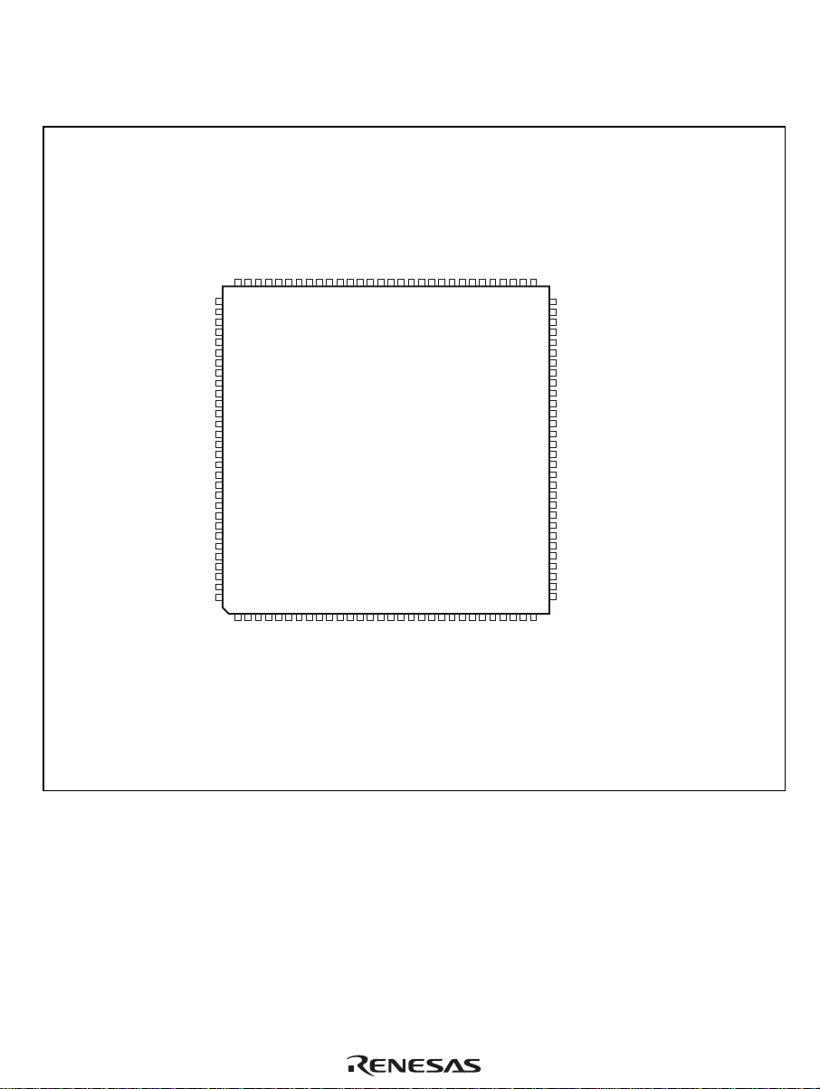
1.3 Pin Assignments
1.3.1 Pin Assignments
Vcc
EXTAL
STBY
P17/IRQ7-A/TCLKD-B
P16/DACK1-A/IRQ6-A/TCLKC-B
MD2
PF7/A23
PB3/CS3/CS7-A
XTAL
PF6/A22
PF5/A21
PF4/A20
P62/TMO2/SCK4/DACK2/IRQ10-B
P63/TMRI3/DREQ3/IRQ11-B
P56/AN6/DA0/IRQ6-B
P57/AN7/DA1/IRQ7-B
PB0/CS0/CS4/CS5-B
PLLVcc
PLLVss
P64/TMCI3/TEND3
P65/TMO3/DACK3
PA0/BREQO/BS-A
PA1/BACK/(RD/WR)
MD0
P50/AN0/IRQ0-B
P51/AN1/IRQ1-B
P52/AN2/IRQ2-B
AVcc
P53/AN3/IRQ3-B
AVss
P54/AN4/IRQ4-B
Vref
P55/AN5/IRQ5-B
MD1
PA2/BREQ/WAIT
PA3/LLWR/LLB
PA4/LHWR/LUB
PA5/RD
PA6/AS/AH/BS-B
Vss
PA7/Bφ
Vcc
P61/TMCI2/RxD4/TEND2/IRQ9-B
P60/TMRI2/TxD4/DREQ2/IRQ8-B
9089888786858483828180797877767574737271706968676665646362
91
92
93
94
95
96
97
98
99
100
101
102
103
104
105
106
107
108
109
110
111
112
113
114
115
116
117
118
119
120
1234567891011121314151617181920212223242526272829
PB2/CS2-A/CS6-A
Vss
WDTOVF
P15/TEND1-A/IRQ5-A/TCLKB-B
Vss
PF3/A19
PF2/A18
VCL
RES
Vss
P14/DREQ1-A/IRQ4-A/TCLKA-B
TFP-120
(top view)
PF1/A17
PF0/A16
PE7/A15
PE6/A14
P12/SCK2/DACK0-A/IRQ2-A
P11/RxD2/TEND0-A/IRQ1-A
P13/ADTRG0/IRQ3-A
Vss
PE5/A13
PE4/A12
PI7/D15
P10/TxD2/DREQ0-A/IRQ0-A
Vcc
PE3/A11
PI6/D14
PI5/D13
PI4/D12
PE1/A9
PE0/A8
PE2/A10
Vss
PI3/D11
PD7/A7
PD6/A6
PI2/D10
PI1/D9
Vss
PD5/A5
PI0/D8
Vcc
PH7/D7
61
60
PH6/D6
59
PH5/D5
58
PH4/D4
57
Vss
56
PH3/D3
55
PH2/D2
54
PH1/D1
53
PH0/D0
52
NMI
51
P37/PO15/TIOCA2/TIOCB2/TCLKD-A
50
P36/PO14/TIOCA2
49
P35/PO13/TIOCA1/TIOCB1/TCLKC-A/DACK1-B
48
P34/PO12/TIOCA1/TEND1-B
47
P33/PO11/TIOCC0/TIOCD0/TCLKB-A/DREQ1-B
46
P32/PO10/TIOCC0/TCLKA-A/DACK0-B
45
P31/PO9/TIOCA0/TIOCB0/TEND0-B
44
Vcc
43
P30/PO8/TIOCA0/DREQ0-B
42
Vss
41
P27/PO7/TIOCA5/TIOCB5
40
P26/PO6/TIOCA5/TMO1/TxD1
39
P25/PO5/TIOCA4/TMCI1/RxD1
38
P24/PO4/TIOCA4/TIOCB4/TMRI1/SCK1
37
P23/PO3/TIOCC3/TIOCD3/IRQ11-A
36
P22/PO2/TIOCC3/TMO0/TxD0/IRQ10-A
P21/PO1/TIOCA3/TMCI0/RxD0/IRQ9-A
35
P20/PO0/TIOCA3/TIOCB3/TMRI0/SCK0/IRQ8-A
34
EMLE
33
PD0/A0
32
PD1/A1
31
30
PD4/A4
PD3/A3
PD2/A2
PB1/CS1/CS2-B/CS5-A/CS6-B/CS7-B
Figure 1.2 Pin Assignments
Rev. 1.00, 03/04, page 3 of 810
Page 44

1.3.2 Pin Configuration in Each Operating Mode
Table 1.1 Pin Configuration in Each Operating Mode
Operating Mode
Pin No. Modes 1 to 7
1 PB1/CS1/CS2-B/CS5-A/CS6-B/CS7-B
2 PB2/CS2-A/CS6-A
3 PB3/CS3/CS7-A
4 MD2
5 PF7/A23
6 PF6/A22
7 PF5/A21
8 PF4/A20
9 PF3/A19
10 VSS
11 PF2/A18
12 PF1/A17
13 PF0/A16
14 PE7/A15
15 PE6/A14
16 PE5/A13
17 VSS
18 PE4/A12
19 VCC
20 PE3/A11
21 PE2/A10
22 PE1/A9
23 PE0/A8
24 PD7/A7
25 PD6/A6
26 VSS
27 PD5/A5
28 PD4/A4
29 PD3/A3
30 PD2/A2
Rev. 1.00, 03/04, page 4 of 810
Page 45

Operating Mode
Pin No. Modes 1 to 7
31 PD1/A1
32 PD0/A0
33 EMLE
34 P20/PO0/TIOCA3/TIOCB3/TMRI0/SCK0/IRQ8-A
35 P21/PO1/TIOCA3/TMCI0/RxD0/IRQ9-A
36 P22/PO2/TIOCC3/TMO0/TxD0/IRQ10-A
37 P23/PO3/TIOCC3/TIOCD3/IRQ11-A
38 P24/PO4/TIOCA4/TIOCB4/TMRI1/SCK1
39 P25/PO5/TIOCA4/TMCI1/RxD1
40 P26/PO6/TIOCA5/TMO1/TxD1
41 P27/PO7/TIOCA5/TIOCB5
42 VSS
43 P30/PO8/TIOCA0/DREQ0-B
44 VCC
45 P31/PO9/TIOCA0/TIOCB0/TEND0-B
46 P32/PO10/TIOCC0/TCLKA-A/DACK0-B
47 P33/PO11/TIOCC0/TIOCD0/TCLKB-A/DREQ1-B
48 P34/PO12/TIOCA1/TEND1-B
49 P35/PO13/TIOCA1/TIOCB1/TCLKC-A/DACK1-B
50 P36/PO14/TIOCA2
51 P37/PO15/TIOCA2/TIOCB2/TCLKD-A
52 NMI
53 PH0/D0
54 PH1/D1
55 PH2/D2
56 PH3/D3
57 VSS
58 PH4/D4
59 PH5/D5
60 PH6/D6
Rev. 1.00, 03/04, page 5 of 810
Page 46

Operating Mode
Pin No. Modes 1 to 7
61 PH7/D7
62 VCC
63 PI0/D8
64 PI1/D9
65 PI2/D10
66 PI3/D11
67 VSS
68 PI4/D12
69 PI5/D13
70 PI6/D14
71 PI7/D15
72 P10/TxD2/DREQ0-A/IRQ0-A
73 P11/RxD2/TEND0-A/IRQ1-A
74 P12/SCK2/DACK0-A/IRQ2-A
75 P13/ADTRG0/IRQ3-A
76 VSS
77 RES
78 VCL
79 P14/DREQ1-A/IRQ4-A/TCLKA-B
80 P15/TEND1-A/IRQ5-A/TCLKB-B
81 WDTOVF
82 VSS
83 XTAL
84 EXTAL
85 VCC
86 P16/DACK1-A/IRQ6-A/TCLKC-B
87 P17/IRQ7-A/TCLKD-B
88 STBY
89 P60/TMRI2/TxD4/DREQ2/IRQ8-B
90 P61/TMCI2/RxD4/TEND2/IRQ9-B
Rev. 1.00, 03/04, page 6 of 810
Page 47

Operating Mode
Pin No. Modes 1 to 7
91 P62/TMO2/SCK4/DACK2/IRQ10-B
92 PLLVCC
93 P63/TMRI3/DREQ3/IRQ11-B
94 PLLVSS
95 P64/TMCI3/TEND3
96 P65/TMO3/DACK3
97 MD0
98 P50/AN0/IRQ0-B
99 P51/AN1/IRQ1-B
100 P52/AN2/IRQ2-B
101 AVCC
102 P53/AN3/IRQ3-B
103 AVSS
104 P54/AN4/IRQ4-B
105 Vref
106 P55/AN5/IRQ5-B
107 P56/AN6/DA0/IRQ6-B
108 P57/AN7/DA1/IRQ7-B
109 MD1
110 PA0/BREQO/BS-A
111 PA1/BACK/(RD/WR)
112 PA2/BREQ/WAIT
113 PA3/LLWR/LLB
114 PA4/LHWR/LUB
115 PA5/RD
116 PA6/AS/AH/BS-B
117 VSS
118 PA7/Bφ
119 VCC
120 PB0/CS0/CS4/CS5-B
Rev. 1.00, 03/04, page 7 of 810
Page 48

1.3.3 Pin Functions
Table 1.2 Pin Functions
Pin No.
Classification Abbreviation
Power supply V
V
V
19, 44, 62,
CC
78 Input Connect to VSS via a 0.1-µF capacitor (place it
CL
10, 17, 26,
SS
PLLVCC 92 Input Power supply pin for the PLL circuits.
PLLVSS 94 Input Ground pin for the PLL circuits.
Clock XTAL 83 Input
EXTAL 84 Input
Bφ 118 Output Outputs the system clock for external devices.
Operating mode
control
MD2
MD1
MD0
System control RES 77 Input Reset signal input pin. This LSI enters the reset
STBY 88 Input This LSI enters hardware standby mode when
EMLE 33 Input Input pin for on-chip emulator enable signal.
(TFP-120) I/O Description
Input Power supply pins. Connect to the system power
85, 119
supply.
close to this pin).
Input Ground pins. Connect to the system power
42, 57, 67,
supply (0 V).
76, 82,
117
Pins for a crystal resonator. External clock can
be input to the EXTAL pin. For a connection
example, see section 19, Clock Pulse Generator.
4
109
97
Input Pins for setting the operating mode. The signal
levels of these pins must not be changed during
operation.
state when this signal goes low.
this signal goes low.
Normally the signal level should be fixed low.
Rev. 1.00, 03/04, page 8 of 810
Page 49

Pin No.
Classification Abbreviation
Address bus A23
A22
A21
A20
A19
A18
A17
A16
A15
A14
A13
A12
A11
A10
A9
A8
A7
A6
A5
A4
A3
A2
A1
A0
Data bus D15
D14
D13
D12
D11
D10
D9
D8
D7
D6
D5
D4
D3
D2
D1
D0
Bus control BREQ 112 Input External bus masters request the bus by this
BREQO 110 Output The internal bus masters request the bus to
(TFP-120) I/O Description
5
6
7
8
9
11
12
13
14
15
16
18
20
21
22
23
24
25
27
28
29
30
31
32
71
70
69
68
66
65
64
63
61
60
59
58
56
55
54
53
Output Output pins for the addresses.
Input/
output
Bidirectional data bus. These pins also output
addresses when accessing the address/data
multiplexed I/O interface space.
signal.
access the external space in the external bus
released state.
Rev. 1.00, 03/04, page 9 of 810
Page 50

Pin No.
Classification Abbreviation
Bus control BACK 111 Output Bus acknowledge signal which indicates that the
BS-A/BS-B 110/116 Output Indicates the start of a bus cycle.
AS 116 Output Strobe signal which indicates that the output
AH 116 Output This signal is used to hold the address when
RD 115 Output Indicates that the basic bus interface space is
RD/WR 111 Output Indicates the direction (input/output) of the data
LHWR 114 Output Strobe signal which indicates that the upper byte
LLWR 113 Output Strobe signal which indicates that the lower byte
LUB 114 Output Strobe signal which indicates that the upper byte
LLB 113 Output Strobe signal which indicates that the lower byte
CS0
CS1
CS2-A/CS2-B
CS3
CS4
CS5-A/CS5-B
CS6-A/CS6-B
CS7-A/CS7-B
WAIT 112 Input Requests wait cycles when accessing the
(TFP-120) I/O Description
bus has been released.
address on the address bus is valid when
accessing the basic bus interface or byte control
SRAM interface space.
accessing the address/data multiplexed I/O
interface space.
being read from.
bus.
(D15 to D8) is valid when accessing the basic
bus interface space.
(D7 to D0) is valid when accessing the basic bus
interface space.
(D15 to D8) is valid when accessing the byte
control SRAM interface space.
(D7 to D0) is valid when accessing the byte
control SRAM interface space.
120
1
2/1
3
120
1/120
2/1
3/1
Output Select signals for areas 7 to 0.
external space.
Rev. 1.00, 03/04, page 10 of 810
Page 51

Pin No.
Classification Abbreviation
Interrupt NMI 52 Input Non-maskable interrupt request signal. When
IRQ11-A/IRQ11-B
IRQ10-A/IRQ10-B
IRQ9-A/IRQ9-B
IRQ8-A/IRQ8-B
IRQ7-A/IRQ7-B
IRQ6-A/IRQ6-B
IRQ5-A/IRQ5-B
IRQ4-A/IRQ4-B
IRQ3-A/IRQ3-B
IRQ2-A/IRQ2-B
IRQ1-A/IRQ1-B
IRQ0-A/IRQ0-B
DMA controller
(DMAC)
DACK0-A/DACK0-B
TEND0-A/TEND0-B
16-bit timer
pulse unit (TPU)
TIOCA0
TIOCA1
TIOCA2
DREQ0-A/DREQ0-B
DREQ1-A/DREQ1-B
DREQ2
DREQ3
DACK1-A/DACK1-B
DACK2
DACK3
TEND1-A/TEND1-B
TEND2
TEND3
TCLKA-A/TCLKA-B
TCLKB-A/TCLKB-B
TCLKC-A/TCLKC-B
TCLKD-A/TCLKD-B
TIOCB0
TIOCC0
TIOCD0
TIOCB1
TIOCB2
(TFP-120) I/O Description
this pin is not in use, this signal must be fixed
high.
37/93
36/91
35/90
34/89
87/108
86/107
80/106
79/104
75/102
74/100
73/99
72/98
72/43
79/47
89
93
74/46
86/49
91
96
73/45
80/48
90
95
46/79
47/80
49/86
51/87
43, 45
45
46, 47
47
48, 49
49
50, 51
51
Input Maskable interrupt request signal.
Input Requests DMAC activation.
Output DMAC single address transfer acknowledge
signal.
Output Indicates DMAC data transfer end.
Input Input pins for the external clocks.
Input/
output
Input/
output
Input/
output
Signals for TGRA_0 to TGRD_0. These are
used for the input capture inputs/output compare
outputs/PWM outputs.
Signals for TGRA_1 and TGRB_1. These are
used for the input capture inputs/output compare
outputs/PWM outputs.
Signals for TGRA_2 and TGRB_2. These are
used for the input capture inputs/output compare
outputs/PWM outputs.
Rev. 1.00, 03/04, page 11 of 810
Page 52

Pin No.
Classification Abbreviation
16-bit timer
pulse unit (TPU)
TIOCA4
TIOCA5
Programmable
pulse generator
(PPG)
8-bit timer
(TMR)
TMCI0
TMRI0
Watchdog timer
(WDT)
TIOCA3
TIOCB3
TIOCC3
TIOCD3
TIOCB4
TIOCB5
PO15
PO14
PO13
PO12
PO11
PO10
PO9
PO8
PO7
PO6
PO5
PO4
PO3
PO2
PO1
PO0
TMO0
TMO1
TMO2
TMO3
TMCI1
TMCI2
TMCI3
TMRI1
TMRI2
TMRI3
WDTOVF 81 Output Output pin for the counter overflow signal in
(TFP-120) I/O Description
34, 35
34
36, 37
37
38, 39
38
40, 41
41
51
50
49
48
47
46
45
43
41
40
39
38
37
36
35
34
36
40
91
96
35
39
90
95
34
38
89
93
Input/
output
Input/
output
Input/
output
Output Output pins for the pulse signals.
Output Output pins for the compare match signals.
Input Input pins for the external clock signals used for
Input Input pins for the counter reset signals.
Signals for TGRA_3 to TGRD_3. These are
used for the input capture inputs/output compare
outputs/PWM outputs.
Signals for TGRA_4 and TGRB_4. These are
used for the input capture inputs/output compare
outputs/PWM outputs.
Signals for TGRA_5 and TGRB_5. These are
used for the input capture inputs/output compare
outputs/PWM outputs.
the counters.
watchdog timer mode.
Rev. 1.00, 03/04, page 12 of 810
Page 53

Pin No.
Classification Abbreviation
Serial
communication
interface (SCI)
RxD0
SCK0
A/D converter AN7
ADTRG0 75 Input Input pin for the external trigger signal to start
D/A converter DA1
A/D converter,
D/A converter
AVSS 103 Input Ground pin for the A/D and D/A converters.
Vref 105 Input Reference power supply pin for the A/D and D/A
I/O port P17
TxD0
TxD1
TxD2
TxD4
RxD1
RxD2
RxD4
SCK1
SCK2
SCK4
AN6
AN5
AN4
AN3
AN2
AN1
AN0
DA0
AVCC 101 Input Analog power supply pin for the A/D and D/A
P16
P15
P14
P13
P12
P11
P10
(TFP-120) I/O Description
36
40
72
89
35
39
73
90
34
38
74
91
108
107
106
104
102
100
99
98
108
107
87
86
80
79
75
74
73
72
Output Output pins for transmit data.
Input Input pins for receive data.
Input/
output
Input Input pins for the analog signals for the A/D
Output Output pins for the analog signals for the D/A
Input/
output
Input/output pins for clock signals.
converter.
A/D conversion.
converter.
converters. When the A/D and D/A converters
are not in use, connect to the system power
supply.
Connect to the system power supply (0 V).
converters. When the A/D and D/A converters
are not in use, connect to the system power
supply.
8-bit input/output pins.
Rev. 1.00, 03/04, page 13 of 810
Page 54

Classification Abbreviation
I/O port P27
P26
P25
P24
P23
P22
P21
P20
P37
P36
P35
P34
P33
P32
P31
P30
P57
P56
P55
P54
P53
P52
P51
P50
P65
P64
P63
P62
P61
P60
PA7
PA6
PA5
PA4
PA3
PA2
PA1
PA0
PB3
PB2
PB1
PB0
Pin No.
(TFP-120) I/O Description
41
40
39
38
37
36
35
34
51
50
49
48
47
46
45
43
108
107
106
104
102
100
99
98
96
95
93
91
90
89
118
116
115
114
113
112
111
110
3
2
1
120
Input/
output
Input/
output
Input 8-bit input/output pins.
Input/
output
Input/
output
Input/
output
8-bit input/output pins.
8-bit input/output pins.
6-bit input/output pins.
8-bit input/output pins.
4-bit input/output pins.
Rev. 1.00, 03/04, page 14 of 810
Page 55

Classification Abbreviation
I/O port PD7
PD6
PD5
PD4
PD3
PD2
PD1
PD0
PE7
PE6
PE5
PE4
PE3
PE2
PE1
PE0
PF7
PF6
PF5
PF4
PF3
PF2
PF1
PF0
PH7
PH6
PH5
PH4
PH3
PH2
PH1
PH0
PI7
PI6
PI5
PI4
PI3
PI2
PI1
PI0
Pin No.
(TFP-120) I/O Description
24
25
27
28
29
30
31
32
14
15
16
18
20
21
22
23
5
6
7
8
9
11
12
13
61
60
59
58
56
55
54
53
71
70
69
68
66
65
64
63
Input/
output
Input/
output
Input/
output
Input/
output
Input/
output
8-bit input/output pins.
8-bit input/output pins.
8-bit input/output pins.
8-bit input/output pins.
8-bit input/output pins.
Rev. 1.00, 03/04, page 15 of 810
Page 56

Rev. 1.00, 03/04, page 16 of 810
Page 57

Section 2 CPU
The H8SX CPU is a high-speed CPU with an internal 32-bit architecture that is upwardcompatible with the H8/300, H8/300H, and H8S CPUs.
The H8SX CPU has sixteen 16-bit general registers, can handle a 4-Gbyte linear address space,
and is ideal for a realtime control system.
2.1 Features
• Upward-compatible with H8/300, H8/300H, and H8S CPUs
Can execute H8/300, H8/300H, and H8S/2000 object programs
• Sixteen 16-bit general registers
Also usable as sixteen 8-bit registers or eight 32-bit registers
• 87 basic instructions
8/16/32-bit arithmetic and logic instructions
Multiply and divide instructions
Bit field transfer instructions
Powerful bit-manipulation instructions
Bit condition branch instructions
Multiply-and-accumulate instruction
• Eleven addressing modes
Register direct [Rn]
Register indirect [@ERn]
Register indirect with displacement [@(d:2,ERn), @(d:16,ERn), or @(d:32,ERn)]
Index register indirect with displacement [@(d:16,RnL.B), @(d:32,RnL.B),
@(d:16,Rn.W), @(d:32,Rn.W), @(d:16,ERn.L), or @(d:32,ERn.L)]
Register indirect with pre-/post-increment or pre-/post-decrement [@+ERn, @−ERn,
@ERn+, or @ERn−]
Absolute address [@aa:8, @aa:16, @aa:24, or @aa:32]
Immediate [#xx:3, #xx:4, #xx:8, #xx:16, or #xx:32]
Program-counter relative [@(d:8,PC) or @(d:16,PC)]
Program-counter relative with index register [@(RnL.B,PC), @(Rn.W,PC), or
@(ERn.L,PC)]
Memory indirect [@@aa:8]
Extended memory indirect [@@vec:7]
CPUSX10A_000120030800 Rev. 1.00, 03/04, page 17 of 810
Page 58

• Two base registers
Vector base register
Short address base register
• 4-Gbyte address space
Program: 4 Gbytes
Data: 4 Gbytes
• High-speed operation
All frequently-used instructions executed in one or two states
8/16/32-bit register-register add/subtract: 1 state
8 × 8-bit register-register multiply: 1 state
16 ÷ 8-bit register-register divide: 10 states
16 × 16-bit register-register multiply: 1 state
32 ÷ 16-bit register-register divide: 18 states
32 × 32-bit register-register multiply: 5 states
32 ÷ 32-bit register-register divide: 18 states
• Four CPU operating modes
Normal mode
Middle mode
Advanced mode
Maximum mode
• Power-down modes
Transition is made by execution of SLEEP instruction
Choice of CPU operating clocks
Notes: 1. Advanced mode is only supported as the CPU operating mode of the H8SX/1657
Group. Normal, middle, and maximum modes are not supported.
2. The multiplier and divider are supported by the H8SX/1657 Group.
Rev. 1.00, 03/04, page 18 of 810
Page 59
2.2 CPU Operating Modes
The H8SX CPU has four operating modes: normal, middle, advanced and maximum modes. For
details on mode settings, see section 3.1, Operating Mode Selection.
Normal mode
Middle mode
CPU operating modes
Advanced mode
Maximum mode
Maximum 64 kbytes for program
and data areas combined
Maximum 16-Mbyte program
area and 64-kbyte data area,
maximum 16 Mbytes for program
and data areas combined
Maximum 16-Mbyte program
area and 4-Gbyte data area,
maximum 4 Gbytes for program
and data areas combined
Maximum 4 Gbytes for program
and data areas combined
Figure 2.1 CPU Operating Modes
2.2.1 Normal Mode
The exception vector table and stack have the same structure as in the H8/300 CPU.
Note: Normal mode is not supported in this LSI.
• Address Space
The maximum address space of 64 kbytes can be accessed.
• Extended Registers (En)
The extended registers (E0 to E7) can be used as 16-bit registers, or as the upper 16-bit
segments of 32-bit registers. When the extended register En is used as a 16-bit register it can
contain any value, even when the corresponding general register Rn is used as an address
register. (If the general register Rn is referenced in the register indirect addressing mode with
pre-/post-increment or pre-/post-decrement and a carry or borrow occurs, however, the value in
the corresponding extended register En will be affected.)
• Instruction Set
All instructions and addressing modes can be used. Only the lower 16 bits of effective
addresses (EA) are valid.
• Exception Vector Table and Memory Indirect Branch Addresses
In normal mode, the top area starting at H'0000 is allocated to the exception vector table. One
branch address is stored per 16 bits. The structure of the exception vector table is shown in
figure 2.2.
Rev. 1.00, 03/04, page 19 of 810
Page 60

H'0000
H'0001
H'0002
H'0003
Reset exception vector
Reset exception vector
Exception
vector table
Figure 2.2 Exception Vector Table (Normal Mode)
The memory indirect (@@aa:8) and extended memory indirect (@@vec:7) addressing modes
are used in the JMP and JSR instructions. An 8-bit absolute address included in the instruction
code specifies a memory location. Execution branches to the contents of the memory location.
• Stack Structure
The stack structure of PC at a subroutine branch and that of PC and CCR at an exception
handling are shown in figure 2.3. The PC contents are saved or restored in 16-bit units.
1
SP
PC
(16 bits)
SP
2
*
(SP )
EXR*
Reserved*
CCR
CCR*3
PC
(16 bits)
1, *3
(a) Subroutine Branch (b) Exception Handling
Notes: 1.
When EXR is not used it is not stored on the stack.
2.
SP when EXR is not used.
3.
Ignored on return.
Figure 2.3 Stack Structure (Normal Mode)
Rev. 1.00, 03/04, page 20 of 810
Page 61

2.2.2 Middle Mode
The program area in middle mode is extended to 16 Mbytes as compared with that in normal
mode.
• Address Space
The maximum address space of 16 Mbytes can be accessed as a total of the program and data
areas. For individual areas, up to 16 Mbytes of the program area or up to 64 kbytes of the data
area can be allocated.
• Extended Registers (En)
The extended registers (E0 to E7) can be used as 16-bit registers, or as the upper 16-bit
segments of 32-bit registers. When the extended register En is used as a 16-bit register (in
other than the JMP and JSR instructions), it can contain any value even when the
corresponding general register Rn is used as an address register. (If the general register Rn is
referenced in the register indirect addressing mode with pre-/post-increment or pre-/postdecrement and a carry or borrow occurs, however, the value in the corresponding extended
register En will be affected.)
• Instruction Set
All instructions and addressing modes can be used. Only the lower 16 bits of effective
addresses (EA) are valid and the upper eight bits are sign-extended.
• Exception Vector Table and Memory Indirect Branch Addresses
In middle mode, the top area starting at H'000000 is allocated to the exception vector table.
One branch address is stored per 32 bits. The upper eight bits are ignored and the lower 24 bits
are stored. The structure of the exception vector table is shown in figure 2.4.
The memory indirect (@@aa:8) and extended memory indirect (@@vec:7) addressing modes
are used in the JMP and JSR instructions. An 8-bit absolute address included in the instruction
code specifies a memory location. Execution branches to the contents of the memory location.
In middle mode, an operand is a 32-bit (longword) operand, providing a 32-bit branch address.
The upper eight bits are reserved and assumed to be H'00.
• Stack Structure
The stack structure of PC at a subroutine branch and that of PC and CCR at an exception
handling are shown in figure 2.5. The PC contents are saved or restored in 24-bit units.
Rev. 1.00, 03/04, page 21 of 810
Page 62
2.2.3 Advanced Mode
The data area is extended to 4 Gbytes as compared with that in middle mode.
• Address Space
The maximum address space of 4 Gbytes can be linearly accessed. For individual areas, up to
16 Mbytes of the program area and up to 4 Gbytes of the data area can be allocated.
• Extended Registers (En)
The extended registers (E0 to E7) can be used as 16-bit registers, or as the upper 16-bit
segments of 32-bit registers or address registers.
• Instruction Set
All instructions and addressing modes can be used.
• Exception Vector Table and Memory Indirect Branch Addresses
In advanced mode, the top area starting at H'00000000 is allocated to the exception vector
table. One branch address is stored per 32 bits. The upper eight bits are ignored and the lower
24 bits are stored. The structure of the exception vector table is shown in figure 2.4.
H'00000000
H'00000001
H'00000002
H'00000003
H'00000004
H'00000005
H'00000006
H'00000007
Reserved
Reset exception vector
Reserved
Exception vector table
Figure 2.4 Exception Vector Table (Middle and Advanced Modes)
The memory indirect (@@aa:8) and extended memory indirect (@@vec:7) addressing modes
are used in the JMP and JSR instructions. An 8-bit absolute address included in the instruction
code specifies a memory location. Execution branches to the contents of the memory location.
In advanced mode, an operand is a 32-bit (longword) operand, providing a 32-bit branch
address. The upper eight bits are reserved and assumed to be H'00.
Rev. 1.00, 03/04, page 22 of 810
Page 63
• Stack Structure
The stack structure of PC at a subroutine branch and that of PC and CCR at an exception
handling are shown in figure 2.5. The PC contents are saved or restored in 24-bit units.
1
SP
SP
Reserved
PC
(24 bits)
(a) Subroutine Branch (b) Exception Handling
2
*
(SP )
EXR*
Reserved*
CCR
PC
(24 bits)
1
3
,
*
Notes: 1.
When EXR is not used it is not stored on the stack.
2.
SP when EXR is not used.
3.
Ignored on return.
Figure 2.5 Stack Structure (Middle and Advanced Modes)
2.2.4 Maximum Mode
The program area is extended to 4 Gbytes as compared with that in advanced mode.
• Address Space
The maximum address space of 4 Gbytes can be linearly accessed.
• Extended Registers (En)
The extended registers (E0 to E7) can be used as 16-bit registers or as the upper 16-bit
segments of 32-bit registers or address registers.
• Instruction Set
All instructions and addressing modes can be used.
• Exception Vector Table and Memory Indirect Branch Addresses
In maximum mode, the top area starting at H'00000000 is allocated to the exception vector
table. One branch address is stored per 32 bits. The structure of the exception vector table is
shown in figure 2.6.
Rev. 1.00, 03/04, page 23 of 810
Page 64
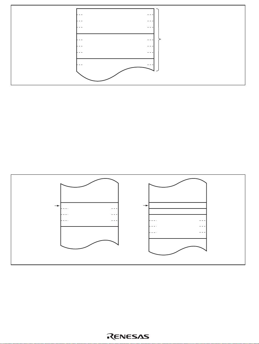
H'00000000
H'00000001
H'00000002
H'00000003
H'00000004
H'00000005
H'00000006
H'00000007
Reset exception vector
Exception vector table
Figure 2.6 Exception Vector Table (Maximum Modes)
The memory indirect (@@aa:8) and extended memory indirect (@@vec:7) addressing modes
are used in the JMP and JSR instructions. An 8-bit absolute address included in the instruction
code specifies a memory location. Execution branches to the contents of the memory location.
In maximum mode, an operand is a 32-bit (longword) operand, providing a 32-bit branch
address.
• Stack Structure
The stack structure of PC at a subroutine branch and that of PC and CCR at an exception
handling are shown in figure 2.7. The PC contents are saved or restored in 32-bit units. The
EXR contents are saved or restored regardless of whether or not EXR is in use.
SP
PC
(32 bits)
(a) Subroutine Branch (b) Exception Handling
Figure 2.7 Stack Structure (Maximum Mode)
Rev. 1.00, 03/04, page 24 of 810
SP
EXR
CCR
PC
(32 bits)
Page 65

2.3 Instruction Fetch
The H8SX CPU has two modes for instruction fetch: 16-bit and 32-bit modes. It is recommended
that the mode be set according to the bus width of the memory in which a program is stored. The
instruction-fetch mode setting does not affect operation other than instruction fetch such as data
accesses. Whether an instruction is fetched in 16- or 32-bit mode is selected by the FETCHMD bit
in SYSCR. For details, see sction 3.2.2, System Control Register (SYSCR).
2.4 Address Space
Figure 2.8 shows a memory map of the H8SX CPU. The address space differs depending on the
CPU operating mode.
Normal mode
H'0000 H'000000
H'007FFF
Program area
Data area
H'FFFF
(64 kbytes)
H'FF8000
H'FFFFFF
Middle mode Advanced mode
H'00000000
Program area
(16 Mbytes)
Data area
(64 kbytes)
H'00FFFFFF
H'FFFFFFFF
Figure 2.8 Memory Map
H'00000000
Program area
(16 Mbytes)
Data area
(4 Gbytes)
H'FFFFFFFF
Maximum mode
Program area
Data area
(4 Gbytes)
Rev. 1.00, 03/04, page 25 of 810
Page 66
2.5 Registers
The H8SX CPU has the internal registers shown in figure 2.9. There are two types of registers:
general registers and control registers. The control registers are the 32-bit program counter (PC),
8-bit extended control register (EXR), 8-bit condition-code register (CCR), 32-bit vector base
register (VBR), 32-bit short address base register (SBR), and 64-bit multiply-accumulate register
(MAC).
General Registers and Extended Registers
15 07 07 0
ER0
ER1
ER2
ER3
ER4
ER5
ER6
ER7 (SP)
Control Registers
31 0
PC
E0
E1
E2
E3
E4
E5
E6
E7
R0H
R1H
R2H
R3H
R4H
R5H
R6H
R7H
R0L
R1L
R2L
R3L
R4L
R5L
R6L
R7L
76543210
UI
HUNZ VCCCR
I
31 012
VBR
31 08
SBR
63 3241
MAC
[Legend]
SP:
PC:
CCR:
I:
UI:
H:
U:
N:
Stack pointer
Program counter
Condition-code register
Interrupt mask bit
User bit or interrupt mask bit
Half-carry flag
User bit
Negative flag
Rev. 1.00, 03/04, page 26 of 810
Sign extension
MACL
Z:
V:
C:
EXR:
T:
I2 to I0:
VBR:
SBR:
MAC:
Zero flag
Overflow flag
Carry flag
Extended control register
Trace bit
Interrupt mask bits
Vector base register
Short address base register
Multiply-accumulate register
Figure 2.9 CPU Registers
7654321
T
————
(Reserved)
(Reserved)
MACH
0
I2 I1 I0EXR
031
Page 67
2.5.1 General Registers
The H8SX CPU has eight 32-bit general registers. These general registers are all functionally alike
and can be used as both address registers and data registers. When a general register is used as a
data register, it can be accessed as a 32-bit, 16-bit, or 8-bit register. Figure 2.10 illustrates the
usage of the general registers.
When the general registers are used as 32-bit registers or address registers, they are designated by
the letters ER (ER0 to ER7).
When the general registers are used as 16-bit registers, the ER registers are divided into 16-bit
general registers designated by the letters E (E0 to E7) and R (R0 to R7). These registers are
functionally equivalent, providing a maximum sixteen 16-bit registers. The E registers (E0 to E7)
are also referred to as extended registers.
When the general registers are used as 8-bit registers, the R registers are divided into 8-bit general
registers designated by the letters RH (R0H to R7H) and RL (R0L to R7L). These registers are
functionally equivalent, providing a maximum sixteen 8-bit registers.
The general registers ER (ER0 to ER7), R (R0 to R7), and RL (R0L to R7L) are also used as index
registers. The size in the operand field determines which register is selected.
The usage of each register can be selected independently.
Address registers
•
32-bit registers
•
32-bit index registers
•
General registers ER
(ER0 to ER7)
16-bit registers
•
General registers E
(E0 to E7)
•
16-bit registers
•
16-bit index registers
•
General registers R
(R0 to R7)
•
•
Figure 2.10 Usage of General Registers
Rev. 1.00, 03/04, page 27 of 810
8-bit registers
General registers RH
(R0H to R7H)
8-bit registers
8-bit index registers
General registers RL
(R0L to R7L)
Page 68

General register ER7 has the function of stack pointer (SP) in addition to its general-register
function, and is used implicitly in exception handling and subroutine branches. Figure 2.11 shows
the stack.
Free area
SP (ER7)
Stack area
Figure 2.11 Stack
2.5.2 Program Counter (PC)
PC is a 32-bit counter that indicates the address of the next instruction the CPU will execute. The
length of all CPU instructions is 16 bits (one word) or a multiple of 16 bits, so the least significant
bit is ignored. (When the instruction code is fetched, the least significant bit is regarded as 0.
Rev. 1.00, 03/04, page 28 of 810
Page 69

2.5.3 Condition-Code Register (CCR)
CCR is an 8-bit register that contains internal CPU status information, including an interrupt mask
(I) and user (UI, U) bits and half-carry (H), negative (N), zero (Z), overflow (V), and carry (C)
flags.
Operations can be performed on the CCR bits by the LDC, STC, ANDC, ORC, and XORC
instructions. The N, Z, V, and C flags are used as branch conditions for conditional branch (Bcc)
instructions.
Initial
Bit Bit Name
7 I 1 R/W Interrupt Mask Bit
6 UI Undefined R/W User Bit or Interrupt Mask Bit
5 H Undefined R/W Half-Carry Flag
4 U Undefined R/W User Bit
3 N Undefined R/W Negative Flag
Value R/W Description
Masks interrupts when set to 1. This bit is set to 1 at
the start of an exception handling.
Can be written to and read from by software using
the LDC, STC, ANDC, ORC, and XORC
instructions. This bit can also be used as an
interrupt mask bit.
When the ADD.B, ADDX.B, SUB.B, SUBX.B,
CMP.B, or NEG.B instruction is executed, this flag is
set to 1 if there is a carry or borrow at bit 3, and
cleared to 0 otherwise. When the ADD.W, SUB.W,
CMP.W, or NEG.W instruction is executed, this flag
is set to 1 if there is a carry or borrow at bit 11, and
cleared to 0 otherwise. When the ADD.L, SUB.L,
CMP.L, or NEG.L instruction is executed, this flag is
set to 1 if there is a carry or borrow at bit 27, and
cleared to 0 otherwise.
Can be written to and read from by software using
the LDC, STC, ANDC, ORC, and XORC
instructions.
Stores the value of the most significant bit (regarded
as sign bit) of data.
Rev. 1.00, 03/04, page 29 of 810
Page 70

Initial
Bit Bit Name
2 Z Undefined R/W Zero Flag
1 V Undefined R/W Overflow Flag
0 C Undefined R/W Carry Flag
Value R/W Description
Set to 1 to indicate zero data, and cleared to 0 to
indicate non-zero data.
Set to 1 when an arithmetic overflow occurs, and
cleared to 0 otherwise.
Set to 1 when a carry occurs, and cleared to 0
otherwise. A carry has the following types:
• Carry from the result of addition
• Borrow from the result of subtraction
• Carry from the result of shift or rotation
The carry flag is also used as a bit accumulator by
bit manipulation instructions.
2.5.4 Extended Control Register (EXR)
EXR is an 8-bit register that contains the trace bit (T) and three interrupt mask bits (I2 to I0).
Operations can be performed on the EXR bits by the LDC, STC, ANDC, ORC, and XORC
instructions.
For details, see section 4, Exception Handling.
Initial
Bit Bit Name
7 T 0 R/W Trace Bit
6 to 3 All 1 R/W Reserved
2
1
0
Rev. 1.00, 03/04, page 30 of 810
I2
I1
I0
Value R/W Description
When this bit is set to 1, a trace exception is
generated each time an instruction is executed.
When this bit is cleared to 0, instructions are
executed in sequence.
These bits are always read as 1.
1
1
1
R/W
R/W
R/W
Interrupt Mask Bits
These bits designate the interrupt mask level (0 to
7).
Page 71

2.5.5 Vector Base Register (VBR)
VBR is a 32-bit register in which the upper 20 bits are valid. The lower 12 bits of this register are
read as 0s. This register is a base address of the vector area for exception handlings other than a
reset and a CPU address error (extended memory indirect is also out of the target). The initial
value is H'00000000. The VBR contents are changed with the LDC and STC instructions.
2.5.6 Short Address Base Register (SBR)
SBR is a 32-bit register in which the upper 24 bits are valid. The lower eight bits are read as 0s. In
8-bit absolute address addressing mode (@aa:8), this register is used as the upper address. The
initial value is H'FFFFFF00. The SBR contents are changed with the LDC and STC instructions.
2.5.7 Multiply-Accumulate Register (MAC)
MAC is a 64-bit register that stores the results of multiply-and-accumulate operations. It consists
of two 32-bit registers denoted MACH and MACL. The lower 10 bits of MACH are valid; the
upper bits are sign extended. The MAC contents are changed with the MAC, CLRMAC, LDMAC,
and STMAC instructions.
2.5.8 Initial Values of CPU Registers
Reset exception handling loads the start address from the vector table into the PC, clears the T bit
in EXR to 0, and sets the I bits in CCR and EXR to 1. The general registers, MAC, and the other
bits in CCR are not initialized. In particular, the initial value of the stack pointer (ER7) is
undefined. The SP should therefore be initialized using an MOV.L instruction executed
immediately after a reset.
Rev. 1.00, 03/04, page 31 of 810
Page 72
2.6 Data Formats
The H8SX CPU can process 1-bit, 4-bit BCD, 8-bit (byte), 16-bit (word), and 32-bit (longword)
data.
Bit-manipulation instructions operate on 1-bit data by accessing bit n (n = 0, 1, 2, …, 7) of byte
operand data. The DAA and DAS decimal-adjust instructions treat byte data as two digits of 4-bit
BCD data.
2.6.1 General Register Data Formats
Figure 2.12 shows the data formats in general registers.
1-bit data
1-bit data
4-bit BCD data
4-bit BCD data
Byte data
Byte data
Word data
Word data
Longword data
15
MSB LSB
31
MSB
[Legend]
ERn:
General register ER
En:
General register E
Rn:
General register R
RnH:
General register RH
RnH
RnL
RnH
RnL
RnH
RnL
Rn
En
ERn
En
7
7 6 5 4 3 2 1 0 Don't care
Don't care 7 6 5 4 3 2 1
43
70
Don't care
7
MSB
Don't care
15
MSB
0
15
16
General register RL
RnL:
Most significant bit
MSB:
Least significant bit
LSB:
0
70
Don’t careUpper Lower
7
Upper
0
Don't care
LSB
70
MSB
Rn
43
0
0
Lower
LSB
0
LSB
0
LSB
Figure 2.12 General Register Data Formats
Rev. 1.00, 03/04, page 32 of 810
Page 73

2.6.2 Memory Data Formats
Figure 2.13 shows the data formats in memory.
The H8SX CPU can access word data and longword data which are stored at any addresses in
memory. When word data begins at an odd address or longword data begins at an address other
than a multiple of 4, a bus cycle is divided into two or more accesses. For example, when
longword data begins at an odd address, the bus cycle is divided into byte, word, and byte
accesses. In this case, these accesses are assumed to be individual bus cycles.
However, instructions to be fetched, word and longword data to be accessed during execution of
the stack manipulation, branch table manipulation, block transfer instructions, and MAC
instruction should be located to even addresses.
When SP (ER7) is used as an address register to access the stack, the operand size should be word
size or longword size.
Data Type Data Format
Address
70
1-bit data
Address L
76543210
Byte data
Word data
Longword data
Address L
Address 2M
Address 2M + 1
Address 2N
Address 2N + 1
Address 2N + 2
Address 2N + 3
MSB LSB
MSB
MSB
Figure 2.13 Memory Data Formats
Rev. 1.00, 03/04, page 33 of 810
LSB
LSB
Page 74
2.7 Instruction Set
The H8SX CPU has 87 types of instructions. The instructions are classified by function as shown
in table 2.1. The arithmetic operation, logic operation, shift, and bit manipulation instructions are
called operation instruction in this manual.
Table 2.1 Instruction Classification
Function Instructions Size Types
Data transfer MOV B/W/L 6
MOVFPE*6, MOVTPE*6 B
POP, PUSH*1 W/L
LDM, STM L
MOVA B/W*2
Block transfer EEPMOV B 3
MOVMD B/W/L
MOVSD B
Arithmetic
operations
DAA, DAS B
ADDS, SUBS L
MULXU, DIVXU, MULXS, DIVXS B/W
MULU, DIVU, MULS, DIVS W/L
MULU/U, MULS/U L
EXTU, EXTS W/L
TAS B
MAC
LDMAC, STMAC
CLRMAC
Logic operations AND, OR, XOR, NOT B/W/L 4
Shift SHLL, SHLR, SHAL, SHAR, ROTL, ROTR, ROTXL, ROTXR B/W/L 8
Bit manipulation BSET, BCLR, BNOT, BTST, BAND, BIAND, BOR, BIOR,
BSET/EQ, BSET/NE, BCLR/EQ, BCLR/NE, BSTZ, BISTZ B
BFLD, BFST B
ADD, ADDX, SUB, SUBX, CMP, NEG, INC, DEC B/W/L 27
B 20
BXOR, BIXOR, BLD, BILD, BST, BIST
Rev. 1.00, 03/04, page 34 of 810
Page 75

Function Instructions Size Types
3
Branch BRA/BS, BRA/BC, BSR/BS, BSR/BC B*
9
Bcc*5, JMP, BSR, JSR, RTS
RTS/L L*5
BRA/S
System control TRAPA, RTE, SLEEP, NOP 10
RTE/L L*5
LDC, STC, ANDC, ORC, XORC B/W/L
Total 87
[Legend]
B: Byte size
W: Word size
L: Longword size
Notes: 1. POP.W Rn and PUSH.W Rn are identical to MOV.W @SP+, Rn and MOV.W Rn,
@−SP.
POP.L ERn and PUSH.L ERn are identical to MOV.L @SP+, ERn and MOV.L ERn,
@−SP.
2. Size of data to be added with a displacement
3. Size of data to specify a branch condition
4. Bcc is the generic designation of a conditional branch instruction.
5. Size of general register to be restored
6. Not available in this LSI.
Rev. 1.00, 03/04, page 35 of 810
Page 76

2.7.1 Instructions and Addressing Modes
Table 2.2 indicates the combinations of instructions and addressing modes that the H8SX CPU can
use.
Table 2.2 Combinations of Instructions and Addressing Modes (1)
Addressing Mode
@(d,
@−ERn/
RnL.B/
@ERn+/
Classification Instruction Size #xx Rn @ERn @(d,ERn)
Data
MOV B/W/L S SD SD SD SD SD SD
Rn.W/
@ERn−/
ERn.L)
@+ERn @aa:8
transfer
B S/D S/D
MOVFPE,
MOVTPE*
B S/D S/D*
12
POP, PUSH W/L S/D S/D*2
LDM, STM L S/D S/D*2
MOVA*4 B/W S S S S S S
EEPMOV B SD*3 Block
transfer
MOVMD B/W/L SD*
MOVSD B SD*3
Arithmetic
operations
ADD, CMP B S D D D D D D D
B S D D D D D D
B D S S S S S S
B SD SD SD SD SD
W/L S SD SD SD SD SD SD
SUB B S D D D D D D
B S D D D D D D
B D S S S S S S
B SD SD SD SD SD
W/L S SD SD SD SD SD SD
ADDX, SUBX B/W/L S SD
B/W/L S SD
B/W/L S SD*5
INC, DEC B/W/L D
ADDS, SUBS L D
DAA, DAS B D
MULXU,
B/W S:4 SD
DIVXU
MULU, DIVU W/L S:4 SD
Rev. 1.00, 03/04, page 36 of 810
@aa:16/
@aa:32
1
3
Page 77

Addressing Mode
@(d,
RnL.B/
Classification
Arithmetic
operations
W/L D D D D D D
EXTU, EXTS W/L D D D D D D
TAS B D
MAC
CLRMAC O
LDMAC S
STMAC D
Logic
operations
W/L D D D D D D
Shift SHLL, SHLR B D D D D D D D
B/W/L*6 D D D D D D
B/W/L*7 D
Bit
manipulation
BAND, BIAND,
Instruction Size #xx Rn @ERn @(d,ERn)
MULXS,
DIVXS
MULS, DIVS W/L S:4 SD
NEG B D D D D D D D
AND, OR, XOR B S D D D D D D
B D S S S S S S
B SD SD SD SD SD
W/L S SD SD SD SD SD SD
NOT B D D D D D D D
ROTL, ROTR
ROTXL,
ROTXR
BSET, BCLR,
BNOT, BTST,
BSET/cc,
BCLR/cc
BOR, BIOR,
BXOR, BIXOR,
BLD, BILD,
BST, BIST,
BSTZ, BISTZ
B/W S:4 SD
B D D D D D D D SHAL, SHAR
W/L D D D D D D
B D D D D
B D D D D
Rn.W/
ERn.L)
@−ERn/
@ERn+/
@ERn−/
@+ERn @aa:8
@aa:16/
@aa:32
Rev. 1.00, 03/04, page 37 of 810
Page 78

Addressing Mode
@(d,
@−ERn/
RnL.B/
@ERn+/
Rn.W/
Classification
manipulation
Branch BRA/BS,
BSR/BS,
System
control
ANDC, ORC,
SLEEP O
NOP O
Instruction Size #xx Rn @ERn @(d,ERn)
BFLD B D S S S Bit
BFST B S D D D
B S S S
BRA/BC*
BSR/BC*
LDC
(CCR, EXR)
LDC
(VBR, SBR)
STC
(CCR, EXR)
STC
(VBR, SBR)
XORC
8
B S S S
8
B/W*9 S S S S S*10 S
L S
B/W*9 D D D D*11 D
L D
B S
@ERn−/
ERn.L)
@+ERn @aa:8
@aa:16/
@aa:32
[Legend]
d: d:16 or d:32
S: Can be specified as a source operand.
D: Can be specified as a destination operand.
SD: Can be specified as either a source or destination operand or both.
S/D: Can be specified as either a source or destination operand.
S:4: 4-bit immediate data can be specified as a source operand.
Notes: 1. Only @aa:16 is available.
2. @ERn+ as a source operand and @−ERn as a destination operand
3. Specified by ER5 as a source address and ER6 as a destination address for data
transfer.
4. Size of data to be added with a displacement
5. Only @ERn− is available
6. When the number of bits to be shifted is 1, 2, 4, 8, or 16
7. When the number of bits to be shifted is specified by 5-bit immediate data or a general
register
8. Size of data to specify a branch condition
9. Byte when immediate or register direct, otherwise, word
10. Only @ERn+ is available
11. Only @−ERn is available
12. Not available in this LSI.
Rev. 1.00, 03/04, page 38 of 810
Page 79

Table 2.2 Combinations of Instructions and Addressing Modes (2)
Addressing Mode
@(RnL.
B/Rn.W/
Classification
Branch BRA/BS,
BSR/BS,
Bcc O
BRA O O
BRA/S O*
JMP O O O O O
BSR O
JSR O O O O O
RTS, RTS/L O
control
Instruction Size @ERn @(d,PC)
O
BRA/BC
O
BSR/BC
TRAPA O System
RTE, RTE/L O
[Legend]
d: d:8 or d:16
Note: * Only @(d:8, PC) is available.
ERn.L,
PC) @aa:24 @ aa:32 @@ aa:8 @@vec:7
Rev. 1.00, 03/04, page 39 of 810
Page 80

2.7.2 Table of Instructions Classified by Function
Tables 2.4 to 2.11 summarize the instructions in each functional category. The notation used in
these tables is defined in table 2.3.
Table 2.3 Operation Notation
Operation Notation Description
Rd General register (destination)*
Rs General register (source)*
Rn General register*
ERn General register (32-bit register)
(EAd) Destination operand
(EAs) Source operand
EXR Extended control register
CCR Condition-code register
VBR Vector base register
SBR Short address base register
N N (negative) flag in CCR
Z Z (zero) flag in CCR
V V (overflow) flag in CCR
C C (carry) flag in CCR
PC Program counter
SP Stack pointer
#IMM Immediate data
disp Displacement
+ Addition
− Subtraction
× Multiplication
÷ Division
∧ Logical AND
∨ Logical OR
⊕ Logical exclusive OR
→ Move
∼ Logical not (logical complement)
:8/:16/:24/:32 8-, 16-, 24-, or 32-bit length
Note: * General registers include 8-bit registers (R0H to R7H, R0L to R7L), 16-bit registers (R0
to R7, E0 to E7), and 32-bit registers (ER0 to ER7).
Rev. 1.00, 03/04, page 40 of 810
Page 81

Table 2.4 Data Transfer Instructions
Instruction Size Function
MOV B/W/L #IMM → (EAd), (EAs) → (EAd)
Transfers data between immediate data, general registers, and memory.
MOVFPE* B (EAs) → Rd
MOVTPE* B Rs → (EAs)
POP W/L @SP+ → Rn
Restores the data from the stack to a general register.
PUSH W/L Rn → @−SP
Saves general register contents on the stack.
LDM L @SP+ → Rn (register list)
Restores the data from the stack to multiple general registers. Two, three,
or four general registers which have serial register numbers can be
specified.
STM L Rn (register list) → @−SP
Saves the contents of multiple general registers on the stack. Two, three,
or four general registers which have serial register numbers can be
specified.
MOVA B/W EA → Rd
Zero-extends and shifts the contents of a specified general register or
memory data and adds them with a displacement. The result is stored in a
general register.
Note: Not available in this LSI.
Rev. 1.00, 03/04, page 41 of 810
Page 82

Table 2.5 Block Transfer Instructions
Instruction Size Function
EEPMOV.B
EEPMOV.W
MOVMD.B B Transfers a data block.
MOVMD.W W Transfers a data block.
MOVMD.L L Transfers a data block.
MOVSD.B B Transfers a data block with zero data detection.
B Transfers a data block.
Transfers byte data which begins at a memory location specified by ER5 to
a memory location specified by ER6. The number of byte data to be
transferred is specified by R4 or R4L.
Transfers byte data which begins at a memory location specified by ER5 to
a memory location specified by ER6. The number of byte data to be
transferred is specified by R4.
Transfers word data which begins at a memory location specified by ER5
to a memory location specified by ER6. The number of word data to be
transferred is specified by R4.
Transfers longword data which begins at a memory location specified by
ER5 to a memory location specified by ER6. The number of longword data
to be transferred is specified by R4.
Transfers byte data which begins at a memory location specified by ER5 to
a memory location specified by ER6. The number of byte data to be
transferred is specified by R4. When zero data is detected during transfer,
the transfer stops and execution branches to a specified address.
Rev. 1.00, 03/04, page 42 of 810
Page 83

Table 2.6 Arithmetic Operation Instructions
z Size Function
ADD
SUB
ADDX
SUBX
INC
DEC
ADDS
SUBS
DAA
DAS
MULXU B/W Rd × Rs → Rd
MULU W/L Rd × Rs → Rd
MULU/U L Rd × Rs → Rd
MULXS B/W Rd × Rs → Rd
MULS W/L Rd × Rs → Rd
MULS/U L Rd × Rs → Rd
DIVXU B/W Rd ÷ Rs → Rd
B/W/L (EAd) ± #IMM → (EAd), (EAd) ± (EAs) → (EAd)
Performs addition or subtraction on data between immediate data, general
registers, and memory. Immediate byte data cannot be subtracted from
byte data in a general register.
B/W/L (EAd) ± #IMM ± C → (EAd), (EAd) ± (EAs) ± C → (EAd)
Performs addition or subtraction with carry on data between immediate
data, general registers, and memory. The addressing mode which
specifies a memory location can be specified as register indirect with postdecrement or register indirect.
B/W/L Rd ± 1 → Rd, Rd ± 2 → Rd
Increments or decrements a general register by 1 or 2. (Byte operands can
be incremented or decremented by 1 only.)
L Rd ± 1 → Rd, Rd ± 2 → Rd, Rd ± 4 → Rd
Adds or subtracts the value 1, 2, or 4 to or from data in a general register.
B Rd (decimal adjust) → Rd
Decimal-adjusts an addition or subtraction result in a general register by
referring to the CCR to produce 2-digit 4-bit BCD data.
Performs unsigned multiplication on data in two general registers: either 8
bits × 8 bits → 16 bits, or 16 bits × 16 bits → 32 bits.
Performs unsigned multiplication on data in two general registers: either 8
bits × 8 bits → 16 bits, or 16 bits × 16 bits → 32 bits.
Performs unsigned multiplication on data in two general registers (32 bits ×
32 bits → upper 32 bits).
Performs signed multiplication on data in two general registers: either 8
bits × 8 bits → 16 bits, or 16 bits × 16 bits → 32 bits.
Performs signed multiplication on data in two general registers: either 16
bits × 16 bits → 16 bits, or 32 bits × 32 bits → 32 bits.
Performs signed multiplication on data in two general registers (32 bits ×
32 bits → upper 32 bits).
Performs unsigned division on data in two general registers: either 16 bits
÷ 8 bits → 8-bit quotient and 8-bit remainder, or 32 bits ÷ 16 bits → 16-bit
quotient and 16-bit remainder.
Rev. 1.00, 03/04, page 43 of 810
Page 84

Instruction Size Function
DIVU W/L Rd ÷ Rs → Rd
Performs unsigned division on data in two general registers: either 16 bits
÷ 16 bits → 16-bit quotient, or 32 bits ÷ 32 bits → 32-bit quotient.
DIVXS B/W Rd ÷ Rs → Rd
Performs signed division on data in two general registers: either 16 bits ÷ 8
bits → 8-bit quotient and 8-bit remainder, or 32 bits ÷ 16 bits → 16-bit
quotient and 16-bit remainder.
DIVS W/L Rd ÷ Rs → Rd
Performs signed division on data in two general registers: either 16 bits ÷
16 bits → 16-bit quotient, or 32 bits ÷ 32 bits → 32-bit quotient.
CMP B/W/L (EAd) − #IMM, (EAd) − (EAs)
Compares data between immediate data, general registers, and memory
and stores the result in CCR.
NEG B/W/L 0 − (EAd) → (EAd)
Takes the two's complement (arithmetic complement) of data in a general
register or the contents of a memory location.
EXTU W/L (EAd) (zero extension) → (EAd)
Performs zero-extension on the lower 8 or 16 bits of data in a general
register or memory to word or longword size.
The lower 8 bits to word or longword, or the lower 16 bits to longword can
be zero-extended.
EXTS W/L (EAd) (sign extension) → (EAd)
Performs sign-extension on the lower 8 or 16 bits of data in a general
register or memory to word or longword size.
The lower 8 bits to word or longword, or the lower 16 bits to longword can
be sign-extended.
TAS B @ERd − 0, 1 → (<bit 7> of @EAd)
Tests memory contents, and sets the most significant bit (bit 7) to 1.
MAC (EAs) × (EAd) + MAC → MAC
Performs signed multiplication on memory contents and adds the result to
MAC.
CLRMAC 0 → MAC
Clears MAC to zero.
LDMAC Rs → MAC
Loads data from a general register to MAC.
STMAC MAC → Rd
Stores data from MAC to a general register.
Rev. 1.00, 03/04, page 44 of 810
Page 85

Table 2.7 Logic Operation Instructions
Instruction Size Function
AND B/W/L (EAd) ∧ #IMM → (EAd), (EAd) ∧ (EAs) → (EAd)
Performs a logical AND operation on data between immediate data,
general registers, and memory.
OR B/W/L (EAd) ∨ #IMM → (EAd), (EAd) ∨ (EAs) → (EAd)
Performs a logical OR operation on data between immediate data, general
registers, and memory.
XOR B/W/L (EAd) ⊕ #IMM → (EAd), (EAd) ⊕ (EAs) → (EAd)
Performs a logical exclusive OR operation on data between immediate
data, general registers, and memory.
NOT B/W/L ∼ (EAd) → (EAd)
Takes the one's complement of the contents of a general register or a
memory location.
Table 2.8 Shift Operation Instructions
Instruction Size Function
SHLL
SHLR
SHAL
SHAR
ROTL
ROTR
ROTXL
ROTXR
B/W/L (EAd) (shift) → (EAd)
Performs a logical shift on the contents of a general register or a memory
location.
The contents of a general register or a memory location can be shifted by
1, 2, 4, 8, or 16 bits. The contents of a general register can be shifted by
any bits. In this case, the number of bits is specified by 5-bit immediate
data or the lower 5 bits of the contents of a general register.
B/W/L (EAd) (shift) → (EAd)
Performs an arithmetic shift on the contents of a general register or a
memory location.
1-bit or 2-bit shift is possible.
B/W/L (EAd) (rotate) → (EAd)
Rotates the contents of a general register or a memory location.
1-bit or 2-bit rotation is possible.
B/W/L (EAd) (rotate) → (EAd)
Rotates the contents of a general register or a memory location with the
carry bit.
1-bit or 2-bit rotation is possible.
Rev. 1.00, 03/04, page 45 of 810
Page 86

Table 2.9 Bit Manipulation Instructions
Instruction Size Function
BSET B 1 → (<bit-No.> of <EAd>)
Sets a specified bit in the contents of a general register or a memory
location to 1. The bit number is specified by 3-bit immediate data or the
lower three bits of a general register.
BSET/cc B if cc, 1 → (<bit-No.> of <EAd>)
If the specified condition is satisfied, this instruction sets a specified bit in a
memory location to 1. The bit number can be specified by 3-bit immediate
data, or by the lower three bits of a general register. The Z flag status can
be specified as a condition.
BCLR B 0 → (<bit-No.> of <EAd>)
Clears a specified bit in the contents of a general register or a memory
location to 0. The bit number is specified by 3-bit immediate data or the
lower three bits of a general register.
BCLR/cc B if cc, 0 → (<bit-No.> of <EAd>)
If the specified condition is satisfied, this instruction clears a specified bit in
a memory location to 0. The bit number can be specified by 3-bit
immediate data, or by the lower three bits of a general register. The Z flag
status can be specified as a condition.
BNOT B ∼ (<bit-No.> of <EAd>) → (<bit-No.> of <EAd>)
Inverts a specified bit in the contents of a general register or a memory
location. The bit number is specified by 3-bit immediate data or the lower
three bits of a general register.
BTST B ∼ (<bit-No.> of <EAd>) → Z
Tests a specified bit in the contents of a general register or a memory
location and sets or clears the Z flag accordingly. The bit number is
specified by 3-bit immediate data or the lower three bits of a general
register.
BAND B C ∧ (<bit-No.> of <EAd>) → C
ANDs the carry flag with a specified bit in the contents of a general register
or a memory location and stores the result in the carry flag. The bit number
is specified by 3-bit immediate data.
BIAND B C ∧ [∼ (<bit-No.> of <EAd>)] → C
ANDs the carry flag with the inverse of a specified bit in the contents of a
general register or a memory location and stores the result in the carry
flag. The bit number is specified by 3-bit immediate data.
BOR B C ∨ (<bit-No.> of <EAd>) → C
ORs the carry flag with a specified bit in the contents of a general register
or a memory location and stores the result in the carry flag. The bit number
is specified by 3-bit immediate data.
Rev. 1.00, 03/04, page 46 of 810
Page 87

Instruction Size Function
BIOR B C ∨ [~ (<bit-No.> of <EAd>)] → C
ORs the carry flag with the inverse of a specified bit in the contents of a
general register or a memory location and stores the result in the carry
flag. The bit number is specified by 3-bit immediate data.
BXOR B C ⊕ (<bit-No.> of <EAd>) → C
Exclusive-ORs the carry flag with a specified bit in the contents of a
general register or a memory location and stores the result in the carry
flag. The bit number is specified by 3-bit immediate data.
BIXOR B C ⊕ [~ (<bit-No.> of <EAd>)] → C
Exclusive-ORs the carry flag with the inverse of a specified bit in the
contents of a general register or a memory location and stores the result in
the carry flag. The bit number is specified by 3-bit immediate data.
BLD B (<bit-No.> of <EAd>) → C
Transfers a specified bit in the contents of a general register or a memory
location to the carry flag. The bit number is specified by 3-bit immediate
data.
BILD B ~ (<bit-No.> of <EAd>) → C
Transfers the inverse of a specified bit in the contents of a general register
or a memory location to the carry flag. The bit number is specified by 3-bit
immediate data.
BST B C → (<bit-No.> of <EAd>)
Transfers the carry flag value to a specified bit in the contents of a general
register or a memory location. The bit number is specified by 3-bit
immediate data.
BSTZ B Z → (<bit-No.> of <EAd>)
Transfers the zero flag value to a specified bit in the contents of a memory
location. The bit number is specified by 3-bit immediate data.
BIST B ∼ C → (<bit-No.> of <EAd>)
Transfers the inverse of the carry flag value to a specified bit in the
contents of a general register or a memory location. The bit number is
specified by 3-bit immediate data.
Rev. 1.00, 03/04, page 47 of 810
Page 88

Instruction Size Function
BISTZ B ∼ Z → (<bit-No.> of <EAd>)
Transfers the inverse of the zero flag value to a specified bit in the
contents of a memory location. The bit number is specified by 3-bit
immediate data.
BFLD B (EAs) (bit field) → Rd
Transfers a specified bit field in memory location contents to the lower bits
of a specified general register.
BFST B Rs → (EAd) (bit field)
Transfers the lower bits of a specified general register to a specified bit
field in memory location contents.
Table 2.10 Branch Instructions
Instruction Size Function
BRA/BS
BRA/BC
BSR/BS
BSR/BC
Bcc Branches to a specified address if the specified condition is satisfied.
BRA/S Branches unconditionally to a specified address after executing the next
JMP Branches unconditionally to a specified address.
BSR Branches to a subroutine at a specified address.
JSR Branches to a subroutine at a specified address.
RTS Returns from a subroutine.
RTS/L Returns from a subroutine, restoring data from the stack to multiple
B Tests a specified bit in memory location contents. If the specified condition
is satisfied, execution branches to a specified address.
B Tests a specified bit in memory location contents. If the specified condition
is satisfied, execution branches to a subroutine at a specified address.
instruction. The next instruction should be a 1-word instruction except for
the block transfer and branch instructions.
general registers.
Rev. 1.00, 03/04, page 48 of 810
Page 89

Table 2.11 System Control Instructions
Instruction Size Function
TRAPA Starts trap-instruction exception handling.
RTE Returns from an exception-handling routine.
RTE/L Returns from an exception-handling routine, restoring data from the stack
to multiple general registers.
SLEEP Causes a transition to a power-down state.
LDC
STC
ANDC B CCR ∧ #IMM → CCR, EXR ∧ #IMM → EXR
ORC B CCR ∨ #IMM → CCR, EXR ∨ #IMM → EXR
XORC B CCR ⊕ #IMM → CCR, EXR ⊕ #IMM → EXR
NOP PC + 2 → PC
B/W #IMM → CCR, (EAs) → CCR, #IMM → EXR, (EAs) → EXR
Loads immediate data or the contents of a general register or a memory
location to CCR or EXR.
Although CCR and EXR are 8-bit registers, word-size transfers are
performed between them and memory. The upper 8 bits are valid.
L Rs → VBR, Rs → SBR
Transfers the general register contents to VBR or SBR.
B/W CCR → (EAd), EXR → (EAd)
Transfers the contents of CCR or EXR to a general register or memory.
Although CCR and EXR are 8-bit registers, word-size transfers are
performed between them and memory. The upper 8 bits are valid.
L VBR → Rd, SBR → Rd
Transfers the contents of VBR or SBR to a general register.
Logically ANDs the CCR or EXR contents with immediate data.
Logically ORs the CCR or EXR contents with immediate data.
Logically exclusive-ORs the CCR or EXR contents with immediate data.
Only increments the program counter.
Rev. 1.00, 03/04, page 49 of 810
Page 90
2.7.3 Basic Instruction Formats
The H8SX CPU instructions consist of 2-byte (1-word) units. An instruction consists of an
operation field (op field), a register field (r field), an effective address extension (EA field), and a
condition field (cc).
Figure 2.14 shows examples of instruction formats.
(1) Operation field only
op
(2) Operation field and register fields
op
(3) Operation field, register fields, and effective address extension
op
EA (disp)
(4) Operation field, effective address extension, and condition field
op cc EA (disp) BRA d:16, etc
rn
rn rm
rm
NOP, RTS, etc.
ADD.B Rn, Rm, etc.
MOV.B @(d:16, Rn), Rm, etc.
Figure 2.14 Instruction Formats
• Operation Field
Indicates the function of the instruction, and specifies the addressing mode and operation to be
carried out on the operand. The operation field always includes the first four bits of the
instruction. Some instructions have two operation fields.
• Register Field
Specifies a general register. Address registers are specified by 3 bits, data registers by 3 bits or
4 bits. Some instructions have two register fields. Some have no register field.
• Effective Address Extension
8, 16, or 32 bits specifying immediate data, an absolute address, or a displacement.
• Condition Field
Specifies the branch condition of Bcc instructions.
Rev. 1.00, 03/04, page 50 of 810
Page 91

2.8 Addressing Modes and Effective Address Calculation
The H8SX CPU supports the 11 addressing modes listed in table 2.12. Each instruction uses a
subset of these addressing modes.
Bit manipulation instructions use register direct, register indirect, or absolute addressing mode to
specify an operand, and register direct (BSET, BCLR, BNOT, and BTST instructions) or
immediate (3-bit) addressing mode to specify a bit number in the operand.
Table 2.12 Addressing Modes
No. Addressing Mode Symbol
1 Register direct Rn
2 Register indirect @ERn
3 Register indirect with displacement @(d:2,ERn)/@(d:16,ERn)/@(d:32,ERn)
4 Index register indirect with displacement @(d:16, RnL.B)/@(d:16,Rn.W)/@(d:16,ERn.L)
@(d:32, RnL.B)/@(d:32,Rn.W)/@(d:32,ERn.L)
5 Register indirect with post-increment @ERn+
Register indirect with pre-decrement @−ERn
Register indirect with pre-increment @+ERn
Register indirect with post-decrement @ERn−
6 Absolute address @aa:8/@aa:16/@aa:24/@aa:32
7 Immediate #xx:3/#xx:4/#xx:8/#xx:16/#xx:32
8 Program-counter relative @(d:8,PC)/@(d:16,PC)
9 Program-counter relative with index register @(RnL.B,PC)/@(Rn.W,PC)/@(ERn.L,PC)
10 Memory indirect @@aa:8
11 Extended memory indirect @@vec:7
2.8.1 Register DirectRn
The operand value is the contents of an 8-, 16-, or 32-bit general register which is specified by the
register field in the instruction code.
R0H to R7H and R0L to R7L can be specified as 8-bit registers.
R0 to R7 and E0 to E7 can be specified as 16-bit registers.
ER0 to ER7 can be specified as 32-bit registers.
Rev. 1.00, 03/04, page 51 of 810
Page 92

2.8.2 Register Indirect@ERn
The operand value is the contents of the memory location which is pointed to by the contents of an
address register (ERn). ERn is specified by the register field of the instruction code.
In advanced mode, if this addressing mode is used in a branch instruction, the lower 24 bits are
valid and the upper 8 bits are all assumed to be 0 (H'00).
2.8.3 Register Indirect with Displacement@(d:2, ERn), @(d:16, ERn), or @(d:32, ERn)
The operand value is the contents of a memory location which is pointed to by the sum of the
contents of an address register (ERn) and a 16- or 32-bit displacement. ERn is specified by the
register field of the instruction code. The displacement is included in the instruction code and the
16-bit displacement is sign-extended when added to ERn.
This addressing mode has a short format (@(d:2, ERn)). The short format can be used when the
displacement is 1, 2, or 3 and the operand is byte data, when the displacement is 2, 4, or 6 and the
operand is word data, or when the displacement is 4, 8, or 12 and the operand is longword data.
2.8.4 Index Register Indirect with Displacement@(d:16,RnL.B), @(d:32,RnL.B),
@(d:16,Rn.W), @(d:32,Rn.W), @(d:16,ERn.L), or @(d:32,ERn.L)
The operand value is the contents of a memory location which is pointed to by the sum of the
following operation result and a 16- or 32-bit displacement: a specified bits of the contents of an
address register (RnL, Rn, ERn) specified by the register field in the instruction code are zeroextended to 32-bit data and multiplied by 1, 2, or 4. The displacement is included in the instruction
code and the 16-bit displacement is sign-extended when added to ERn. If the operand is byte data,
ERn is multiplied by 1. If the operand is word or longword data, ERn is multiplied by 2 or 4,
respectively.
2.8.5 Register Indirect with Post-Increment, Pre-Decrement, Pre-Increment,
or Post-Decrement@ERn+, @−ERn, @+ERn, or @ERn−
• Register indirect with post-increment@ERn+
The operand value is the contents of a memory location which is pointed to by the contents of
an address register (ERn). ERn is specified by the register field of the instruction code. After
the memory location is accessed, 1, 2, or 4 is added to the address register contents and the
sum is stored in the address register. The value added is 1 for byte access, 2 for word access, or
4 for longword access.
Rev. 1.00, 03/04, page 52 of 810
Page 93

• Register indirect with pre-decrement@−ERn
The operand value is the contents of a memory location which is pointed to by the following
operation result: the value 1, 2, or 4 is subtracted from the contents of an address register
(ERn). ERn is specified by the register field of the instruction code. After that, the operand
value is stored in the address register. The value subtracted is 1 for byte access, 2 for word
access, or 4 for longword access.
• Register indirect with pre-increment@+ERn
The operand value is the contents of a memory location which is pointed to by the following
operation result: the value 1, 2, or 4 is added to the contents of an address register (ERn). ERn
is specified by the register field of the instruction code. After that, the operand value is stored
in the address register. The value added is 1 for byte access, 2 for word access, or 4 for
longword access.
• Register indirect with post-decrement@ERn−
The operand value is the contents of a memory location which is pointed to by the contents of
an address register (ERn). ERn is specified by the register field of the instruction code. After
the memory location is accessed, 1, 2, or 4 is subtracted from the address register contents and
the remainder is stored in the address register. The value subtracted is 1 for byte access, 2 for
word access, or 4 for longword access.
If the contents of a general register which is also used as an address register is written to memory
using this addressing mode, data to be written is the contents of the address register after
calculating an effective address.
2.8.6 Absolute Address@aa:8, @aa:16, @aa:24, or @aa:32
The operand value is the contents of a memory location which is pointed to by an absolute address
included in the instruction code.
There are 8-bit (@aa:8), 16-bit (@aa:16), 24-bit (@aa:24), and 32-bit (@aa:32) absolute
addresses.
To access the data area, the absolute address of 8 bits (@aa:8), 16 bits (@aa:16), or 32 bits
(@aa:32) is used. For an 8-bit absolute address, the upper 24 bits are specified by SBR. For a 16bit absolute address, the upper 16 bits are sign-extended. A 32-bit absolute address can access the
entire address space.
To access the program area, the absolute address of 24 bits (@aa:24) or 32 bits (@aa:32) is used.
For a 24-bit absolute address, the upper 8 bits are all assumed to be 0 (H'00).
Table 2.13 shows the accessible absolute address ranges.
Rev. 1.00, 03/04, page 53 of 810
Page 94

Table 2.13 Absolute Address Access Ranges
Absolute
Address
Data area 8 bits
(@aa:8)
16 bits
(@aa:16)
32 bits
(@aa:32)
Program area 24 bits
(@aa:24)
32 bits
(@aa:32)
Normal
Mode
A consecutive 256-byte area (the upper address is set in SBR)
H'0000 to
H'FFFF
H'000000 to
H'00000000 to
Middle
Mode
H'000000 to
H'007FFF,
H'FF8000 to
H'FFFFFF
H'FFFFFF
Advanced
Mode
H'00000000 to H'00007FFF,
H'FFFF8000 to H'FFFFFFFF
H'00000000 to H'FFFFFFFF
H'00000000 to H'00FFFFFF
H'00FFFFFF
Maximum
Mode
H'00000000 to
H'FFFFFFFF
2.8.7 Immediate#xx
The operand value is 8-bit (#xx:8), 16-bit (#xx:16), or 32-bit (#xx:32) data included in the
instruction code.
This addressing mode has short formats in which 3- or 4-bit immediate data can be used.
When the size of immediate data is less than that of the destination operand value (byte, word, or
longword) the immediate data is zero-extended.
The ADDS, SUBS, INC, and DEC instructions contain immediate data implicitly. Some bit
manipulation instructions contain 3-bit immediate data in the instruction code, for specifying a bit
number. The BFLD and BFST instructions contain 8-bit immediate data in the instruction code,
for specifying a bit field. The TRAPA instruction contains 2-bit immediate data in the instruction
code, for specifying a vector address.
2.8.8 Program-Counter Relative@(d:8, PC) or @(d:16, PC):
This mode is used in the Bcc and BSR instructions. The operand value is a 32-bit branch address,
which is the sum of an 8- or 16-bit displacement in the instruction code and the 32-bit address of
the PC contents. The 8-bit or 16-bit displacement is sign-extended to 32 bits when added to the PC
contents. The PC contents to which the displacement is added is the address of the first byte of the
next instruction, so the possible branching range is −126 to +128 bytes (−63 to +64 words) or
−32766 to +32768 bytes (−16383 to +16384 words) from the branch instruction. The resulting
value should be an even number. In advanced mode, only the lower 24 bits of this branch address
are valid; the upper 8 bits are all assumed to be 0 (H'00).
Rev. 1.00, 03/04, page 54 of 810
Page 95
2.8.9 Program-Counter Relative with Index Register@(RnL.B, PC), @(Rn.W, PC), or
@(ERn.L, PC)
This mode is used in the Bcc and BSR instructions. The operand value is a 32-bit branch address,
which is the sum of the following operation result and the 32-bit address of the PC contents: the
contents of an address register specified by the register field in the instruction code (RnL, Rn, or
ERn) is zero-extended and multiplied by 2. The PC contents to which the displacement is added is
the address of the first byte of the next instruction. In advanced mode, only the lower 24 bits of
this branch address are valid; the upper 8 bits are all assumed to be 0 (H'00).
2.8.10 Memory Indirect@@aa:8
This mode can be used by the JMP and JSR instructions. The operand value is a branch address,
which is the contents of a memory location pointed to by an 8-bit absolute address in the
instruction code.
The upper bits of an 8-bit absolute address are all assumed to be 0, so the address range is 0 to 255
(H'0000 to H'00FF in normal mode, H'000000 to H'0000FF in other modes).
In normal mode, the memory location is pointed to by word-size data and the branch address is 16
bits long. In other modes, the memory location is pointed to by longword-size data. In middle or
advanced mode, the first byte of the longword-size data is assumed to be all 0 (H'00).
Note that the top part of the address range is also used as the exception handling vector area. A
vector address of an exception handling other than a reset or a CPU address error can be changed
by VBR.
Figure 2.15 shows an example of specification of a branch address using this addressing mode.
Specified
by @aa:8
Branch address
(a) Normal Mode (b) Advanced Mode
Specified
by @aa:8
Reserved
Branch address
Figure 2.15 Branch Address Specification in Memory Indirect Mode
Rev. 1.00, 03/04, page 55 of 810
Page 96

2.8.11 Extended Memory Indirect@@vec:7
This mode can be used by the JMP and JSR instructions. The operand value is a branch address,
which is the contents of a memory location pointed to by the following operation result: the sum
of 7-bit data in the instruction code and the value of H'80 is multiplied by 2 or 4.
The address range to store a branch address is H'0100 to H'01FF in normal mode and H'000200 to
H'0003FF in other modes. In assembler notation, an address to store a branch address is specified.
In normal mode, the memory location is pointed to by word-size data and the branch address is 16
bits long. In other modes, the memory location is pointed to by longword-size data. In middle or
advanced mode, the first byte of the longword-size data is assumed to be all 0 (H'00).
2.8.12 Effective Address Calculation
Tables 2.14 and 2.15 show how effective addresses are calculated in each addressing mode. The
lower bits of the effective address are valid and the upper bits are ignored (zero extended or sign
extended) according to the CPU operating mode.
The valid bits in middle mode are as follows:
• The lower 16 bits of the effective address are valid and the upper 16 bits are sign-extended for
the transfer and operation instructions.
• The lower 24 bits of the effective address are valid and the upper eight bits are zero-extended
for the branch instructions.
Rev. 1.00, 03/04, page 56 of 810
Page 97

Table 2.14 Effective Address Calculation for Transfer and Operation Instructions
No.
Addressing Mode and Instruction Format Effective Address Calculation Effective Address (EA)
1
Immediate
IMM
Register direct
2
opoprm rn
Register indirect
3
op
r
4
Register indirect with 16-bit displacement
op
r
disp
Register indirect with 32-bit displacement
op
r
disp
31 0 31 0
General register contents
31 0
General register contents
31 15
Sign extension
31 0
General register contents
disp
disp
31 0
0
+
31 0
+
5
Index register indirect with 16-bit displacement
op
r
disp
Index register indirect with 32-bit displacement
op
r
disp
Register indirect with post-increment or post-decrement
6
op
r
Register indirect with pre-increment or pre-decrement
op
r
8-bit absolute address
7
op
aa
16-bit absolute address
op
aa
32-bit absolute address
op
aa
31 0
Zero extension
Contents of general register (RL, R, or ER)
31 15
Sign extension
31 0
Zero extension
Contents of general register (RL, R, or ER)
31
31
31
31 07
31 15
Sign extension
31
disp
General register contents
General register contents
One extension
aa
1, 2, or 4
disp
1, 2, or 4
1, 2, or 4
1, 2, or 4
aa
aa
×
31 0
+
0
×
31 0
0
+
0
31 0
±
0
31 0
±
31 0
0
31 0
0
31 0
Rev. 1.00, 03/04, page 57 of 810
Page 98
Table 2.15 Effective Address Calculation for Branch Instructions
No.
Addressing Mode and Instruction Format Effective Address Calculation Effective Address (EA)
Register indirect
1
r
op
Program-counter relative with 8-bit displacement
2
op
disp
Program-counter relative with 16-bit displacement
op
disp
31 0 31
General register contents
31 0
31 7 0
31 0
31 15 0
Sign extension
Sign extension
PC contents
PC contents
+
disp
disp
+
31 0
31 0
0
Program-counter relative with index register
3
op
r
24-bit absolute address
4
op
32-bit absolute address
op
aa
Memory indirect
5
op aa
6
Extended memory indirect
op
vec
aa aa
31 0
Zero extension
Contents of general register (RL, R, or ER)
31
Zero
31 23 0
extension
31
31 0
31
31
31
31
PC contents
Zero extension
Memory contents
Zero extension
Memory contents
aa
7
aa
17vec
2 or 4
×
2
31 0
0
+
31 0
31 0
0
31 0
0
0
×
0
31 0
0
2.8.13 MOVA Instruction
The MOVA instruction stores the effective address in a general register.
1. Firstly, data is obtained by the addressing mode shown in item 2of table 2.14.
2. Next, the effective address is calculated using the obtained data as the index by the addressing
mode shown in item 5 of table 2.14. The obtained data is used instead of the general register.
The result is stored in a general register. For details, see H8SX Family Programming Manual.
Rev. 1.00, 03/04, page 58 of 810
Page 99

2.9 Processing States
The H8SX CPU has five main processing states: the reset state, exception-handling state, program
execution state, bus-released state, and program stop state. Figure 2.16 indicates the state
transitions.
• Reset state
In this state the CPU and internal peripheral modules are all initialized and stopped. When the
RES input goes low, all current processing stops and the CPU enters the reset state. All
interrupts are masked in the reset state. Reset exception handling starts when the RES signal
changes from low to high. For details, refer to section 4, Exception Handling.
The reset state can also be entered by a watchdog timer overflow when available.
• Exception-handling state
The exception-handling state is a transient state that occurs when the CPU alters the normal
processing flow due to activation of an exception source, such as, a reset, trace, interrupt, or
trap instruction. The CPU fetches a start address (vector) from the exception handling vector
table and branches to that address. For further details, refer to section 4, Exception Handling.
• Program execution state
In this state the CPU executes program instructions in sequence.
• Bus-released state
The bus-released state occurs when the bus has been released in response to a bus request from
a bus master other than the CPU. While the bus is released, the CPU halts operations.
• Program stop state
This is a power-down state in which the CPU stops operating. The program stop state occurs
when a SLEEP instruction is executed or the CPU enters hardware standby mode. For details,
refer to section 20, Power-Down Modes.
Rev. 1.00, 03/04, page 59 of 810
Page 100
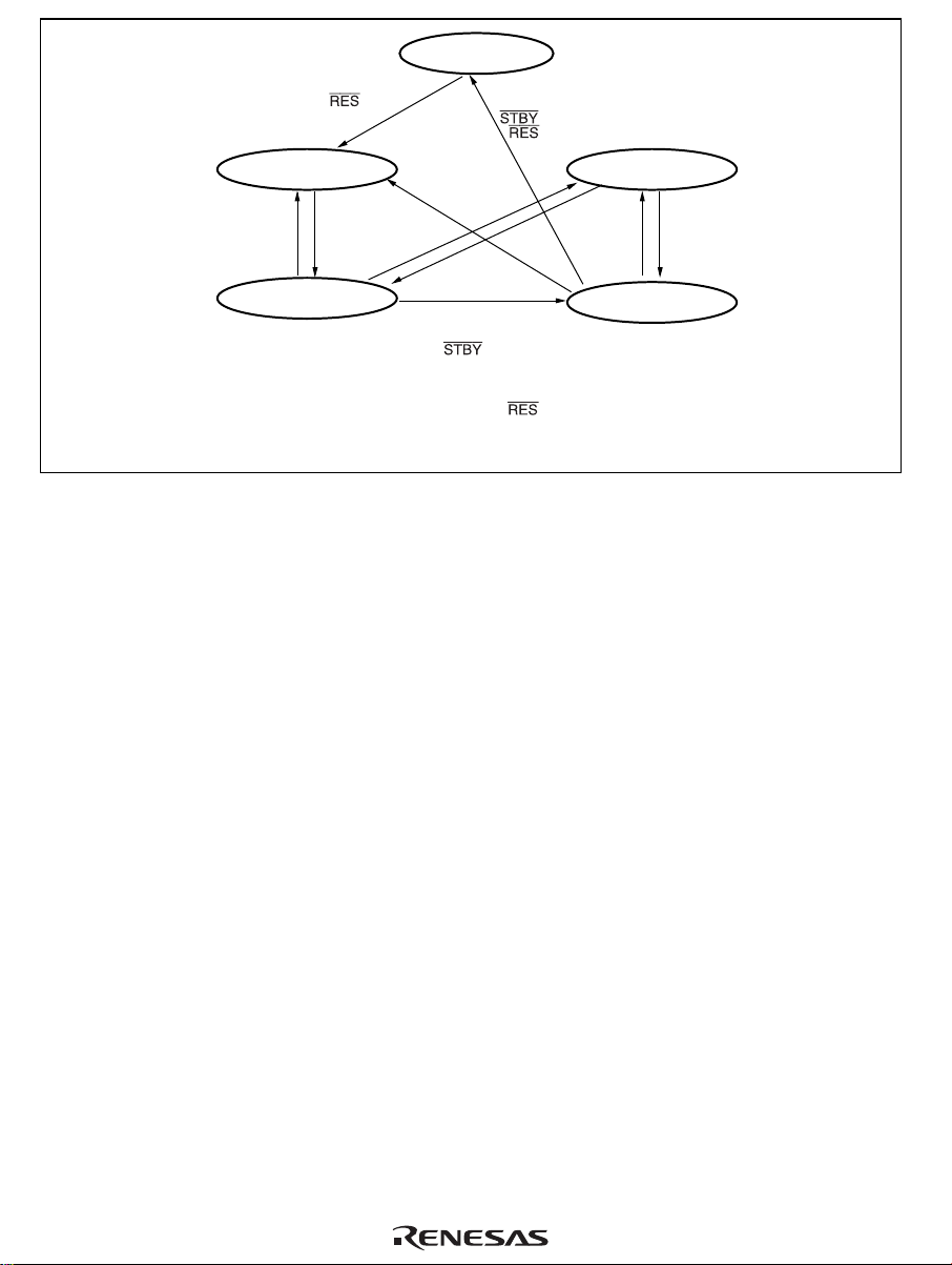
Reset state*
Exception-handling
Request for exception
handling
Program execution
Notes:
*
= high
state
End of exception
handling
state
In any state, when the signal goes low, the hardware standby
mode is entered.
From any state except hardware standby mode, a transition to the
reset state occurs whenever the
can also be made to the reset state when the watchdog timer overflows.
Interrupt
request
End of
bus request
SLEEP instruction
= high,
= low
Bus
request
Bus request
signal goes low. A transition
Bus-released state
End of bus request
Program stop state
Figure 2.16 State Transitions
Rev. 1.00, 03/04, page 60 of 810
 Loading...