

Page 1
R0E53033ACFG90
Converter Board for Connecting R8C/33A Group 32-pin 0.8mm pitch LQFP
User’s Manual
* NQPACK, YQPACK, YQSOCKET, YQ-GUIDE, HQPACK, TQPACK, TQSOCKET, CSSOCKET, CSPLUG/W and LSPACK are
trademarks of Tokyo Eletech Corporation.
CAUTION
Renesas Tools Homepage http://www.renesas.com/tools
Rev.1.00
Jun. 01, 2008
REJ10J1872-0100
If the requirements shown in the "CAUTION" sentences are ignored,
the equipment may cause personal injury or damage to the products.
(1/4)
Page 2
1. Outline
The R0E53033ACFG90 is a converter board for connecting the
signals of the MCU unit R0E521300MCU00 for R8C/Tiny
Series to a foot pattern for 32-pin 0.8mm pitch LQFP of
R8C/33A group.
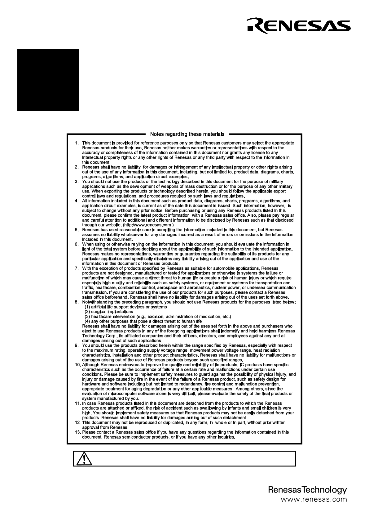
2. Package Components (See Figure 1)
Check to see if the R0E53033ACFG90 package has all the
following contents before using this product.
(1) R0E53033ACFG90 converter board........................... 1 pc.
(2) YQPACK032SA
(3) NQPACK032SA
(4) YQ-GUIDE
(made by Tokyo Eletech Corporation).......... 1 pc.
(made by Tokyo Eletech Corporation) ........ 1 pc.
(made by Tokyo Eletech Corporation) ...............4 pcs.
(5) R0E53033ACFG90 User's Manual (this manual)
3. Specifications
Table 1 Specifications
PLQP0032GB-A:
Applicable package
formerly 32P6U-A
(32-pin 0.8mm pitch LQFP)
Insertion/removal
iterations of connector
50 times guaranteed
4. Usage (See Figure 2)
The R0E53033ACFG90 can be used for debugging and
on-board evaluation in common by mounting the
NQPACK032SA on the user system.
(1) For debugging
Mount the NQPACK032SA on the foot pattern of the user
system and attach the YQPACK032SA on it. In addition,
connect the R0E53033ACFG90 to the YQPACK032SA,
and then connect the flexible cable R0E001000FLX10 of
the emulator to the upper connector of the
R0E53033ACFG90.
(2) For on-board evaluation
Mount an MCU with on-chip flash memory or one-time
PROM and the HQPACK032SA (not included) in order
on the NQPACK032SA on the user system.
Before using the R0E53033ACFG90, be sure to read "7.
Precautions" on page 4.
R0E53033ACFG90
YQ-GUIDE (×4)
YQPACK032SA
NQPACK032SA
Figure 1 Package components of the R0E53033ACFG90
(1) For debugging
Flexible cable
R0E001000FLX10
(2) For on-board
evaluation
R0E53033ACFG90
HQPACK032SA
(not included)
YQ-GUIDE (×4)
YQPACK032SA
NQPACK032SA
32-pin 0.8mm pitch
foot pattern
●: No.1 pin
Be sure to align the pins.
FLASH MCU, etc.
Figure 2 Usage of the R0E53033ACFG90
(2/4)
Page 3

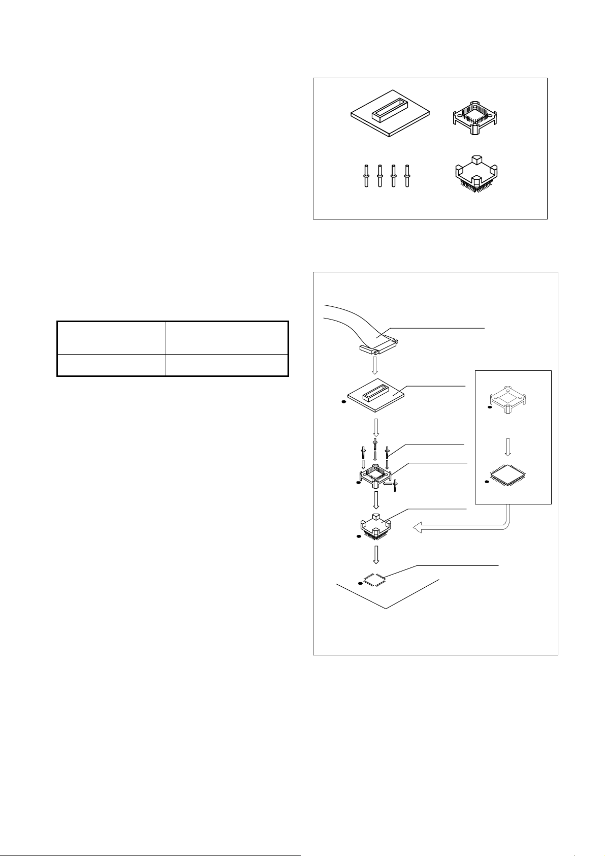
5. Connection Procedure (See Figure 3)
The procedure for connecting the R0E53033ACFG90 is shown
below.
(1) Mount the NQPACK032SA on the user system.
(2) Attach the YQPACK032SA on the NQPACK032SA.
(3) Secure the four corners of the YQPACK032SA with the
YQ-GUIDEs.
● Do not use the screws included with the
YQPACK032SA for fixing the YQPACK032SA.
● Do NOT use the screwdriver included with the
NQPACK032SA for fixing the YQ-GUIDEs. That is
used only for the HQPACK032SA.
(4) Mount the R0E53033ACFG90 on the YQPACK032SA.
(5) Connect the flexible cable R0E001000FLX10 of the
emulator to the R0E53033ACFG90.
Flexible cable
R0E001000FLX10
(5)
R0E53033ACFG90
Use a slotted screwdriver.
(4)
YQ-GUIDE(×4)
YQPACK032SA
(3)
(2)
(1)
NQPACK032SA
32-pin 0.8mm pitch
foot pattern
●: No.1 pin
Be sure to align the pins.
Figure 3 Connection procedure of the R0E53033ACFG90
6. External Dimensions and a Sample Foot Pattern
22.00
MADE IN JAPAN
CN1
Pb Free
50
TP1
100
1
51
TP2
R0E53033ACFG90
REV.A
10.65
38.00
10.65
16.50
0.50
0.80
6.80
6.80
10.00
2.65
Figure 4 External dimensions and a sample foot pattern of the R0E53033ACFG90
2.65
(3/4)
10.00
Unit: mm
Page 4

7. Precautions
CAUTION
Cautions to Be Taken for This Product:
z When connecting the YQPACK032SA, be sure to use the included YQ-GUIDEs.
z Do NOT use the screws included with the YQPACK032SA for connecting the YQPACK032SA.
IMPORTANT
Notes on This Product:
z We cannot accept any request for repair.
z For purchasing the NQPACK032SA, YQPACK032SA, HQPACK032SA, contact the following:
Tokyo Eletech Corporation http://www.tetc.co.jp/e_index.htm
z For inquiries about the product or the contents of this manual, contact your local distributor.
Renesas Tools Homepage http://www.renesas.com/tools
8. Correspondence of Connectors CN1
Table 2 Correspondence of the connectors
CN1 Pin No. IC1 CN1 Pin No. IC1
1 - 100 2 - 99 3 - 98 4 - 97 5 19 96 18
6 20 95 17
7 21 94 16
8 22 93 -
9 23 92 10 24 91 11 - 90 12 - 89 13 - 88 14 - 87 15 - 86 16 - 85 17 - 84 18 - 83 19 - 82 20 25 81 15
21 26 80 22 27 79 23 28 78 24 29 77 25 30 76 26 - 75 27 31 74 14
28 32 73 13
29 - 72 12
30 - 71 31 - 70 32 - 69 33 - 68 34 - 67 35 - 66 11
36 - 65 10
37 - 64 38 - 63 9
39 - 62 8
40 - 61 41 - 60 42 1 59 43 2 58 44 - 57 45 - 56 7
46 3 55 6
47 4 54 5
48 - 53 49 - 52 50 - 51 -
(-: No connection or signals in the emulator)
(4/4)
 Loading...