

Page 1
Release Note
R20UT4965EC0100 Rev.1.0.0 Page 1 of 8
Mar.31.21
QE for AFE[RA] V1.0.0
Release Note
Thank you very much for using the QE for AFE[RA] V1.0.0.
This release note covers product installation, restrictions, and so on. Please read this document before using
the product.
Contents
1. About QE for AFE .................................................................................................................... 2
1.1 Summary ................................................................................................................................................. 2
1.2 Functions ................................................................................................................................................. 2
1.3 Supported Environment ........................................................................................................................... 2
1.4 Supported Microcontrollers ..................................................................................................................... 2
2. Installation and Uninstallation .................................................................................................. 3
2.1 Installing This Product ............................................................................................................................. 3
2.2 Updating This Product ............................................................................................................................. 3
2.3 Uninstalling This Product ......................................................................................................................... 3
3. Notes / Restrictions.................................................................................................................. 4
3.1 Usage Considerations ............................................................................................................................. 4
3.1.1 Notes on SDADC24 Configuration ........................................................................................................ 4
3.1.2 Notes on ADC16 Configuration ............................................................................................................. 5
3.1.3 Notes on “stop AFE tuning” Operation Failure ...................................................................................... 5
3.1.4 Notes on Setting DAC8/DAC12 Output Pin Function ........................................................................... 5
3.1.5 Notes on Tuning Time on [AD Monitor] Tab .......................................................................................... 5
3.1.6 Notes on Tuning ADC16 on [AD Monitor] Tab ...................................................................................... 6
3.1.7 Notes on UART connection ................................................................................................................... 6
3.1.8 Notes on switching monitoring targets in the [AD Monitor] tab ............................................................. 7
Revision History .............................................................................................................................. 8
Page 2

QE for AFE[RA] V1.0.0 Release Note
R20UT4965EC0100 Rev.1.0.0 Page 2 of 8
Mar.31.21
1. About QE for AFE
1.1 Summary
QE for AFE[RA] is an evaluation tool for embedded system development that performs graphical tuning with
an integrated analog front end (AFE). Using this tool, you can configure AFE registers, write register into
evaluation board and monitor the A/D conversion results in a waveform.
QE for AFE[RA] is a standalone version tool (.exe) running on local PC. To use this tool, you firstly need an
evaluation board. QE for AFE[RA] communicates with the evaluation board by a USB cable connecting
between PC and board.
1.2 Functions
The main functions are listed below:
1. Connect and operate the evaluation board
2. Set AFE related registers with GUI
3. Display graphics of AD conversion result and digital filter frequency response
1.3 Supported Environment
Host PC: Windows10 (64 bit)
Evaluation board: EK-RA2A1
Sample project: The sample project attached in the application note (RA2A1 Groupe Board Control
Program for “QE for AFE”: R01AN5795EJ0100) must be loaded by e2 studio and run on the evaluation
board. Please refer to the application note for details.
1.4 Supported Microcontrollers
• RA Family (only MCUs that incorporate the AFE)
⎯ RA2A Series: RA2A1
Page 3
QE for AFE[RA] V1.0.0 Release Note
R20UT4965EC0100 Rev.1.0.0 Page 3 of 8
Mar.31.21
2. Installation and Uninstallation
2.1 Installing This Product
QE for AFE[RA] is provided as a compressed package (.zip). Follow the procedure below to use this product:
1. Extract “.zip” file to a user-specified location on the PC.
Note: Please do not put the tool under OS program folder (C:\Program Files)
2. Start this product by double clicking “\eclipse\ qe-afe.exe”.
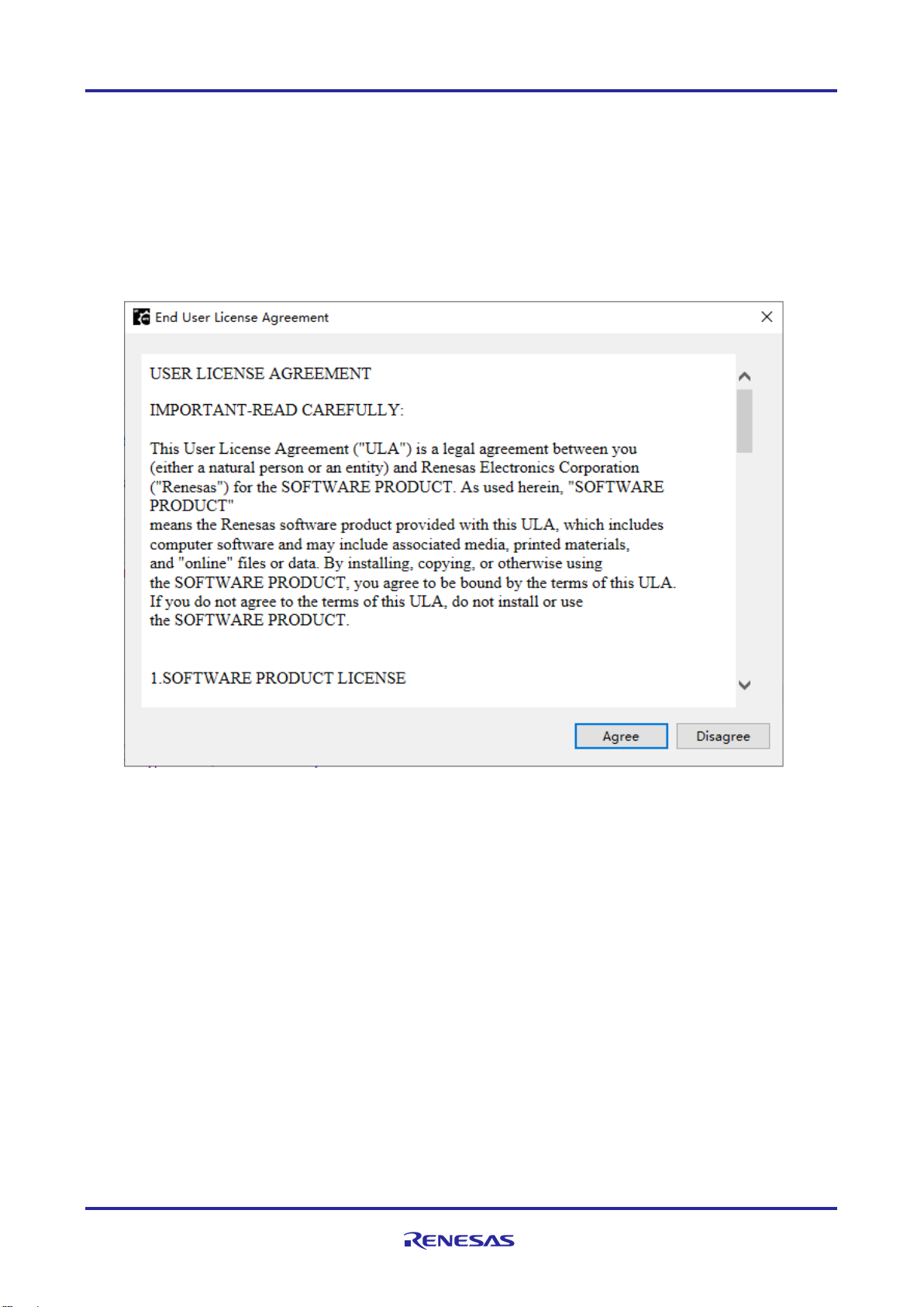
3. For the first time this product starts, there is a dialog of license agreement. After checking the license,
you can select “Agree” or “Disagree”.
Figure 2-1. License agreement dialog
4. If “Agree” is selected in above step, the product is launched then you can use it; if “Disagree” is selected
in above step, the product won’t be launched.
2.2 Updating This Product
If you have already used this product, you can update it in the same way as the procedure for installation.
2.3 Uninstalling This Product
Delete the entire folder in which .zip package is extracted.
Page 4

QE for AFE[RA] V1.0.0 Release Note
R20UT4965EC0100 Rev.1.0.0 Page 4 of 8
Mar.31.21
3. Notes / Restrictions
3.1 Usage Considerations
Please pay attention to the following items.
3.1.1 Notes on SDADC24 Configuration
The SDADC24 reference clock which is input on the GUI must be consistent with the actual clock used on
the evaluation board, otherwise SDADC24 can’t work as expected and the graphics displayed in QE for AFE
isn’t correct.
Figure 3-1 SDADC24 clock setting
When using USB communication with evaluation board, please set STC1.CLKDIV as “1/12”, set SDADCCLK
as 48MHz; when using UART communication with evaluation board, please set STC1.CLKDIV as “1/16”, set
SDADCCLK as 64MHz. For detailed explanation, please refer to the application note (RA2A1 Groupe Board
Control Program for “QE for AFE”: R01AN5795EJ0100).
Page 5

QE for AFE[RA] V1.0.0 Release Note
R20UT4965EC0100 Rev.1.0.0 Page 5 of 8
Mar.31.21
3.1.2 Notes on ADC16 Configuration
To display the ADC16 conversion results using QE for AFE, please increase the number of enabled
channels and set the sampling time longer (see Figure 3-2). If LED1 on the evaluation board is always on,
which means the board is not operating properly, please restart QE for AFE and reset the sample project to
try again.
Figure 3-2 ADC16 configuration setting
3.1.3 Notes on “stop AFE tuning” Operation Failure
Occasionally user click “stop AFE tuning” button on [AD Monitor] tab but the tuning doesn’t stop. As a
workaround of this case, please click “Disconnect” button to disconnect QE for AFE with evaluation board.
Then click “Connect” button after resetting the evaluation board.
3.1.4 Notes on Setting DAC8/DAC12 Output Pin Function
QE for AFE V1.0.0 doesn’t support to set PmnPFS register which is used to set DAC8/DAC12 output pin
function. Please set PmnPFS register in firmware program manually when you need to use DAC8/DAC12
output pin.
3.1.5 Notes on Tuning Time on [AD Monitor] Tab
When tuning on [AD Monitor] tab, QE for AFE obtains A/D conversion values from the evaluation board. If
the tuning time is very long, too much data will lead to the host PC memory overflow. So, QE for AFE V1.0.0
supports tuning time no more than 1 hour. If tuning operates for more than 1 hour, the tool will stop tuning
automatically and output a message to inform user that the tuning time can’t exceed 1 hour.
Enable more channels
Set the sampling time longer
Page 6

QE for AFE[RA] V1.0.0 Release Note
R20UT4965EC0100 Rev.1.0.0 Page 6 of 8
Mar.31.21
3.1.6 Notes on Tuning ADC16 on [AD Monitor] Tab
Please note the follow procedure by which QE for AFE get ADC16 conversion result from the evaluation
board:
1) After user click “Start AFE tuning” button on [AD Monitor] Tab in QE for AFE, ADC16 starts conversion
on evaluation board.
2) On evaluation board, when the A/D conversion result buffer is full, the sample project stops ADC16
conversion and send response to QE for AFE.
3) QE for AFE starts to read data from evaluation board until the result buffer is empty.
4) QE for AFE restart ADC16 conversion, the procedure goes to 2)
Above 2) to 4) is internal communication between QE for AFE and sample project, which will continue until
user click “stop AFE tuning” button.
3.1.7 Notes on UART connection
Please note the following items when using UART connection.
1) After reset of the evaluation board, please set bitrate as 1000000bps in the [ConnectSetting] dialog, then
click “connect” button.
Figure 3-3 Bitrate setting
2) After successful connection with evaluation board, you can open the [ConnectSetting] dialog to change
the bitrate setting. 1000000bps, 1500000bps, 2000000bps, or 3000000bps can be input manually or
selected from the combo box.
3) It's rare case that the current bitrate information displayed in [ConnectSetting] dialog is invalid. When
you met this case, please confirm the message output in [Console] window firstly. If the message is
“[Info]Set bitrate successfully”, the invalid information can be ignored. If bitrate change failed, please try
it again.
Figure 3-4 Invalid current bitrate information
Page 7
QE for AFE[RA] V1.0.0 Release Note
R20UT4965EC0100 Rev.1.0.0 Page 7 of 8
Mar.31.21
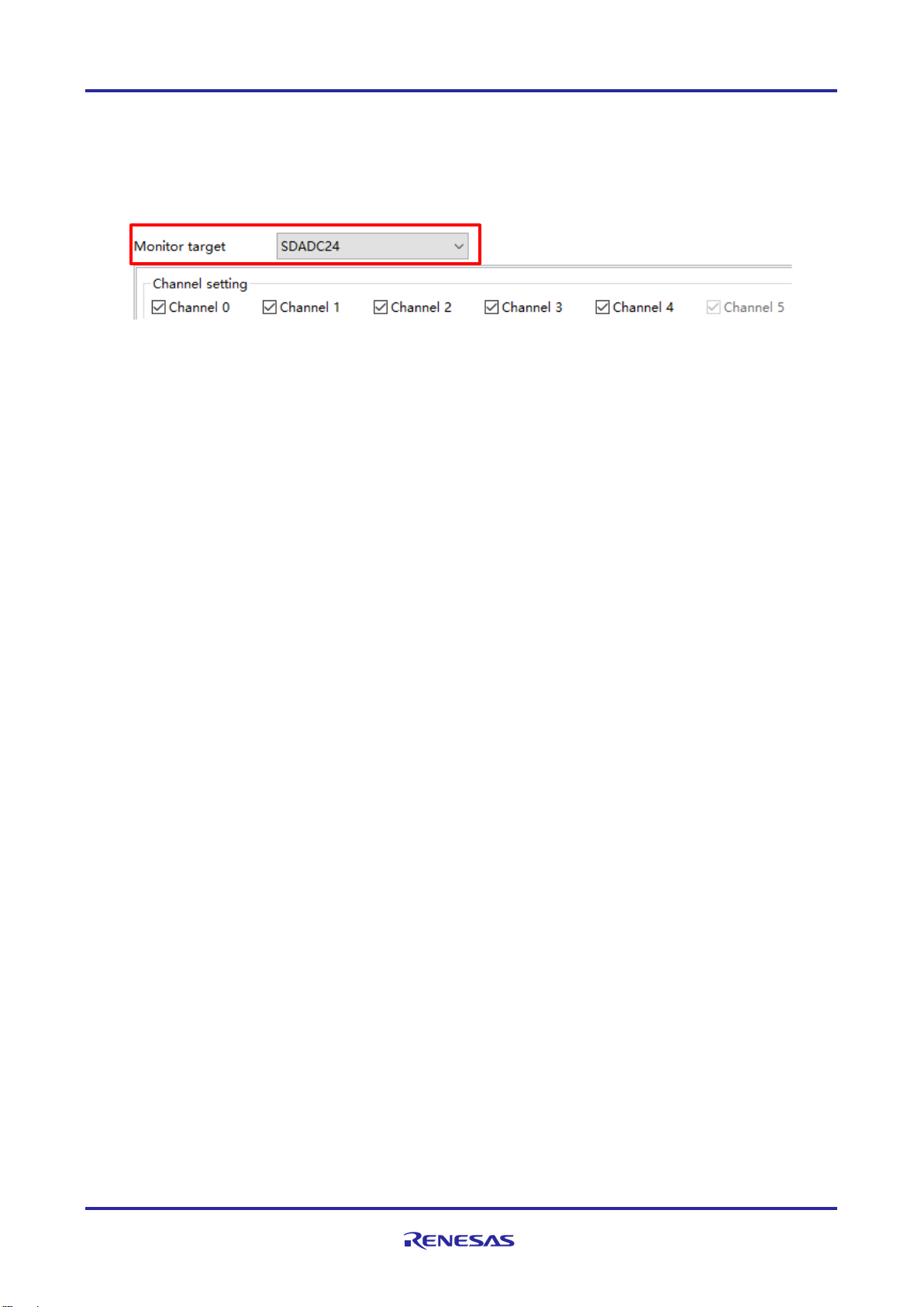
3.1.8 Notes on switching monitoring targets in the [AD Monitor] tab
When the [Monitor target] is switched in the [AD Monitor] tab, the channel selected in the [Channel setting]
may be not correctly. As a workaround, please click [Start AFE tuning] button once. It can correct [Channel
setting] automatically when AFE tuning starts.
Figure 3-5 Monitor target setting
Page 8
QE for AFE[RA] V1.0.0 Release Note
R20UT4965EC0100 Rev.1.0.0 Page 8 of 8
Mar.31.21
Revision History
Rev.
Date
Description
Page
Summary
1.0.0
Mar.31.21
-
First edition issued.
Page 9

General Precautions in the Handling of Microprocessing Unit and Microcontroller Unit Products
The following usage notes are applicable to all Microprocessing unit and Microcontroller unit products from Renesas. For detailed usage notes on the
products covered by this document, refer to the relevant sections of the document as well as any technical updates that have been issued for the products.
1. Precaution against Electrostatic Discharge (ESD)
A strong electrical field, when exposed to a CMOS device, can cause destruction of the gate oxide and ultimately degrade the device operation. Steps
must be taken to stop the generation of static electricity as much as possible, and quickly dissipate it when it occurs. Environmental control must be
adequate. When it is dry, a humidifier should be used. This is recommended to avoid using insulators that can easily build up static electricity.
Semiconductor devices must be stored and transported in an anti-static container, static shielding bag or conductive material. All test and
measurement tools including work benches and floors must be grounded. The operator must also be grounded using a wrist strap. Semiconductor
devices must not be touched with bare hands. Similar precautions must be taken for printed circuit boards with mounted semiconductor devices.
2. Processing at power-on
The state of the product is undefined at the time when power is supplied. The states of internal circuits in the LSI are indeterminate and the states of
register settings and pins are undefined at the time when power is supplied. In a finished product where the reset signal is applied to the external reset
pin, the states of pins are not guaranteed from the time when power is supplied until the reset process is completed. In a similar way, the states of pins
in a product that is reset by an on-chip power-on reset function are not guaranteed from the time when power is supplied until the power reaches the
level at which resetting is specified.
3. Input of signal during power-off state
Do not input signals or an I/O pull-up power supply while the device is powered off. The current injection that results from input of such a signal or I/O
pull-up power supply may cause malfunction and the abnormal current that passes in the device at this time may cause degradation of internal
elements. Follow the guideline for input signal during power-off state as described in your product documentation.
4. Handling of unused pins
Handle unused pins in accordance with the directions given under handling of unused pins in the manual. The input pins of CMOS products are
generally in the high-impedance state. In operation with an unused pin in the open-circuit state, extra electromagnetic noise is induced in the vicinity of
the LSI, an associated shoot-through current flows internally, and malfunctions occur due to the false recognition of the pin state as an input signal
become possible.
5. Clock signals
After applying a reset, only release the reset line after the operating clock signal becomes stable. When switching the clock signal during program
execution, wait until the target clock signal is stabilized. When the clock signal is generated with an external resonator or from an external oscillator
during a reset, ensure that the reset line is only released after full stabilization of the clock signal. Additionally, when switching to a clock signal
produced with an external resonator or by an external oscillator while program execution is in progress, wait until the target clock signal is stable.
6. Voltage application waveform at input pin
Waveform distortion due to input noise or a reflected wave may cause malfunction. If the input of the CMOS device stays in the area between VIL
(Max.) and VIH (Min.) due to noise, for example, the device may malfunction. Take care to prevent chattering noise from entering the device when the
input level is fixed, and also in the transition period when the input level passes through the area between VIL (Max.) and VIH (Min.).
7. Prohibition of access to reserved addresses
Access to reserved addresses is prohibited. The reserved addresses are provided for possible future expansion of functions. Do not access these
addresses as the correct operation of the LSI is not guaranteed.
8. Differences between products
Before changing from one product to another, for example to a product with a different part number, confirm that the change will not lead to problems.
The characteristics of a microprocessing unit or microcontroller unit products in the same group but having a different part number might differ in terms
of internal memory capacity, layout pattern, and other factors, which can affect the ranges of electrical characteristics, such as characteristic values,
operating margins, immunity to noise, and amount of radiated noise. When changing to a product with a different part number, implement a systemevaluation test for the given product.
Page 10

© 2021 Renesas Electronics Corporation. All rights reserved.
Notice
1. Descriptions of circuits, software and other related information in this document are provided only to illustrate the operation of semiconductor products
and application examples. You are fully responsible for the incorporation or any other use of the circuits, software, and information in the design of your
product or system. Renesas Electronics disclaims any and all liability for any losses and damages incurred by you or third parties arising from the use
of these circuits, software, or information.
2. Renesas Electronics hereby expressly disclaims any warranties against and liability for infringement or any other claims involving patents, copyrights,
or other intellectual property rights of third parties, by or arising from the use of Renesas Electronics products or technical information described in this
document, including but not limited to, the product data, drawings, charts, programs, algorithms, and application examples.
3. No license, express, implied or otherwise, is granted hereby under any patents, copyrights or other intellectual property rights of Renesas Electronics
or others.
4. You shall be responsible for determining what licenses are required from any third parties, and obtaining such licenses for the lawful import, export,
manufacture, sales, utilization, distribution or other disposal of any products incorporating Renesas Electronics products, if required.
5. You shall not alter, modify, copy, or reverse engineer any Renesas Electronics product, whether in whole or in part. Renesas Electronics disclaims any
and all liability for any losses or damages incurred by you or third parties arising from such alteration, modification, copying or reverse engineering.
6. Renesas Electronics products are classified according to the following two quality grades: “Standard” and “High Quality”. The intended applications for
each Renesas Electronics product depends on the product’s quality grade, as indicated below.
"Standard": Computers; office equipment; communications equipment; test and measurement equipment; audio and visual equipment; home
electronic appliances; machine tools; personal electronic equipment; industrial robots; etc.
"High Quality": Transportation equipment (automobiles, trains, ships, etc.); traffic control (traffic lights); large-scale communication equipment; key
financial terminal systems; safety control equipment; etc.
Unless expressly designated as a high reliability product or a product for harsh environments in a Renesas Electronics data sheet or other Renesas
Electronics document, Renesas Electronics products are not intended or authorized for use in products or systems that may pose a direct threat to
human life or bodily injury (artificial life support devices or systems; surgical implantations; etc.), or may cause serious property damage (space
system; undersea repeaters; nuclear power control systems; aircraft control systems; key plant systems; military equipment; etc.). Renesas Electronics
disclaims any and all liability for any damages or losses incurred by you or any third parties arising from the use of any Renesas Electronics product
that is inconsistent with any Renesas Electronics data sheet, user’s manual or other Renesas Electronics document.
7. No semiconductor product is absolutely secure. Notwithstanding any security measures or features that may be implemented in Renesas Electronics
hardware or software products, Renesas Electronics shall have absolutely no liability arising out of any vulnerability or security breach, including but
not limited to any unauthorized access to or use of a Renesas Electronics product or a system that uses a Renesas Electronics product. RENESAS
ELECTRONICS DOES NOT WARRANT OR GUARANTEE THAT RENESAS ELECTRONICS PRODUCTS, OR ANY SYSTEMS CREATED USING
RENESAS ELECTRONICS PRODUCTS WILL BE INVULNERABLE OR FREE FROM CORRUPTION, ATTACK, VIRUSES, INTERFERENCE,
HACKING, DATA LOSS OR THEFT, OR OTHER SECURITY INTRUSION (“Vulnerability Issues”). RENESAS ELECTRONICS DISCLAIMS ANY AND
ALL RESPONSIBILITY OR LIABILITY ARISING FROM OR RELATED TO ANY VULNERABILITY ISSUES. FURTHERMORE, TO THE EXTENT
PERMITTED BY APPLICABLE LAW, RENESAS ELECTRONICS DISCLAIMS ANY AND ALL WARRANTIES, EXPRESS OR IMPLIED, WITH
RESPECT TO THIS DOCUMENT AND ANY RELATED OR ACCOMPANYING SOFTWARE OR HARDWARE, INCLUDING BUT NOT LIMITED TO
THE IMPLIED WARRANTIES OF MERCHANTABILITY, OR FITNESS FOR A PARTICULAR PURPOSE.
8. When using Renesas Electronics products, refer to the latest product information (data sheets, user’s manuals, application no tes, “General Notes for
Handling and Using Semiconductor Devices” in the reliability handbook, etc.), and ensure that usage conditions are within the ranges specified by
Renesas Electronics with respect to maximum ratings, operating power supply voltage range, heat dissipation characteristics, installation, etc. Renesas
Electronics disclaims any and all liability for any malfunctions, failure or accident arising out of the use of Renesas Electronics products outside of such
specified ranges.
9. Although Renesas Electronics endeavors to improve the quality and reliability of Renesas Electronics products, semiconductor products have specific
characteristics, such as the occurrence of failure at a certain rate and malfunctions under certain use conditions. Unless designated as a high reliability
product or a product for harsh environments in a Renesas Electronics data sheet or other Renesas Electronics document, Renesas Electronics
products are not subject to radiation resistance design. You are responsible for implementing safety measures to guard against the possibility of bodily
injury, injury or damage caused by fire, and/or danger to the public in the event of a failure or malfunction of Renesas Electronics products, such as
safety design for hardware and software, including but not limited to redundancy, fire control and malfunction prevention, appropriate treatment for
aging degradation or any other appropriate measures. Because the evaluation of microcomputer software alone is very difficult and impractical, you are
responsible for evaluating the safety of the final products or systems manufactured by you.
10. Please contact a Renesas Electronics sales office for details as to environmental matters such as the environmental compatibility of each Renesas
Electronics product. You are responsible for carefully and sufficiently investigating applicable laws and regulations that regulate the inclusion or use of
controlled substances, including without limitation, the EU RoHS Directive, and using Renesas Electronics products in compliance with all these
applicable laws and regulations. Renesas Electronics disclaims any and all liability for damages or losses occurring as a result of your noncompliance
with applicable laws and regulations.
11. Renesas Electronics products and technologies shall not be used for or incorporated into any products or systems whose manufacture, use, or sale is
prohibited under any applicable domestic or foreign laws or regulations. You shall comply with any applicable export control laws and regulations
promulgated and administered by the governments of any countries asserting jurisdiction over the parties or transactions.
12. It is the responsibility of the buyer or distributor of Renesas Electronics products, or any other party who distributes, disposes of, or otherwise sells or
transfers the product to a third party, to notify such third party in advance of the contents and conditions set forth in this document.
13. This document shall not be reprinted, reproduced or duplicated in any form, in whole or in part, without prior written consent of Renesas Electronics.
14. Please contact a Renesas Electronics sales office if you have any questions regarding the information contained in this document or Renesas
Electronics products.
(Note1) “Renesas Electronics” as used in this document means Renesas Electronics Corporation and also includes its directly or indirectly controlled
subsidiaries.
(Note2) “Renesas Electronics product(s)” means any product developed or manufactured by or for Renesas Electronics.
(Rev.5.0-1 October 2020)
Corporate Headquarters
Contact information
TOYOSU FORESIA, 3-2-24 Toyosu,
Koto-ku, Tokyo 135-0061, Japan
www.renesas.com
For further information on a product, technology, the most up-to-date
version of a document, or your nearest sales office, please visit:
www.renesas.com/contact/.
Trademarks
Renesas and the Renesas logo are trademarks of Renesas Electronics
Corporation. All trademarks and registered trademarks are the property
of their respective owners.
 Loading...