

Page 1
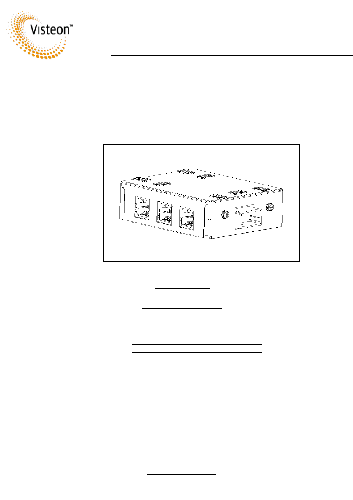
Multimedia Service Manual
for the Control Module used on the Renault Rear
Seat Entertainment System
Control Module
Control Module
Control Module Control Module
Part Number 4035241
Part Number 4035241
Part Number 4035241Part Number 4035241
Document no. 30-900-00015
Produced by: Visteon Technical Service
Download from: http://euro.evisteon.com
Issue
Issue Remarks
IssueIssue
2002-11-28 First Issue
Printed Copies are Uncontrolled.
Printed Copies are Uncontrolled.
Rear Seat Entertainment System Control Module
for the Renault Scenic, Laguna and Espace
Printed Copies are Uncontrolled.Printed Copies are Uncontrolled.
About this Document
About this Document
About this DocumentAbout this Document
Operations
Remarks
RemarksRemarks
CONFIDENTIAL
30-900-00015 Issued 2002-11-28 http:/euro.evisteon.com © Copyright Visteon 2002
Page 2
Service Manual – Renault System
A. Initial Inspection and Test.
1. Read the dealer fault report.
2. Examine the module. Note any bent or missing connector pins or other obvious damage.
3. Plug the module into the test kit and test as follows. Note any faults found.
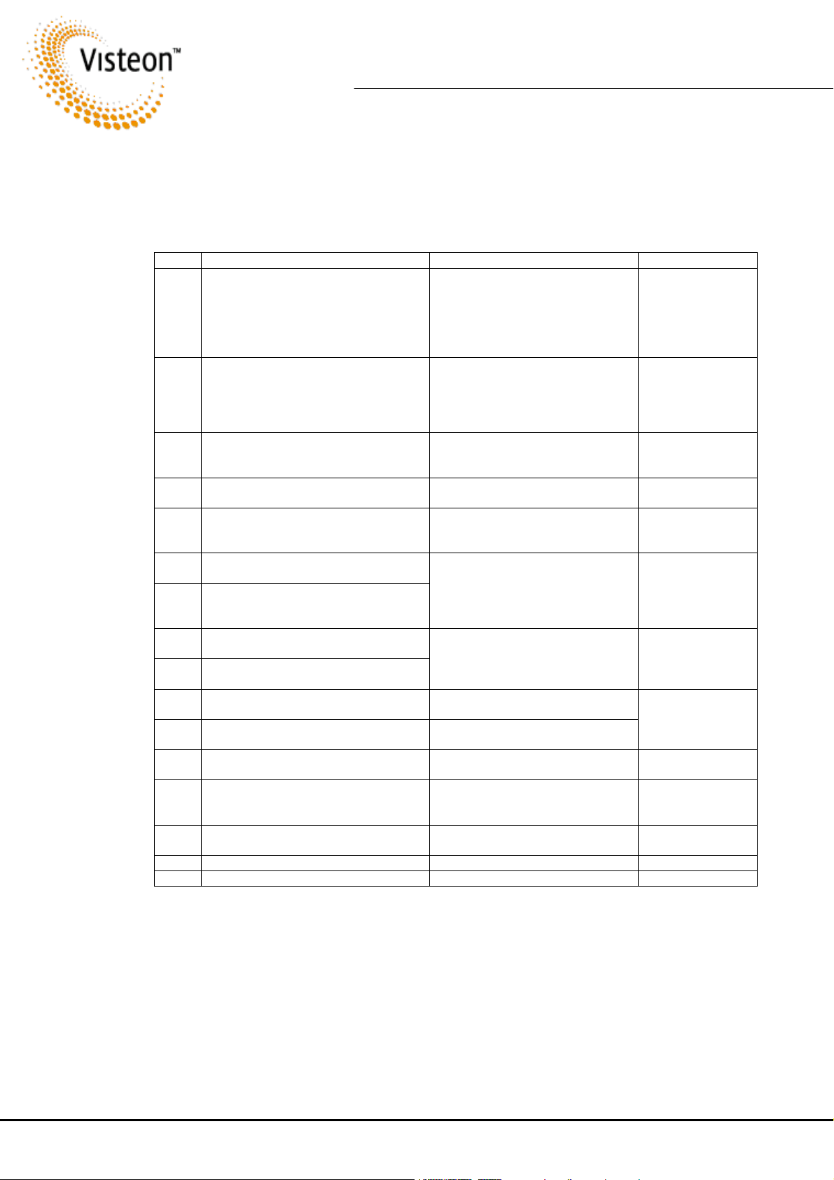
Step Procedure Check that . . Verification
1 Connect the control module to the test
kit. Plug the output from the DVD into
CN1 (see figure 1) on the control
module. Connect a 12.5 V DC supply to
The DVD switches on.
the permanent and ignition inputs of the
test kit.
2 Aim the remote control at TFT screen A
and press 'POWER'
Both TFT screens come on
3 Press 'MENU' on the remote. Navigate
to 'MEDIA SELECT' then press 'ENTER'.
The menu appears on TFT A. Menu chip.
Select DVD and press ENTER again.
4 Aim the remote at TFT screen B and
select DVD as per step 2 above.
The menu appears on TFT B
5 Insert a DVD disk into the DVD player. Check that the DVD displays on
both screens and there is sound on
both channels.
6 Aim the controller at TFT A, press Stop,
wait and then press PLAY.
7 Aim the controller at TFT B and press
Menu. Press Stop and then PLAY as
The DVD pauses then continues to
play each time.
above.
10 Plug the DVD output into CN2. Use the
remote to select AUX 1 on both screens.
11 Plug the DVD output into CN3. Use the
remote to select AUX 2 on both screens.
17 With the remote aimed at Screen A
The picture from the DVD appears
on TFT A and TFT B as each
selection is made and there is sound
on both channels.
Colour scale appears on screen
select COLOUR on the DISPLAY menu.
18 Vary intensity from high to low colour.
Set back to mid-range.
19 Select BRIGHTNESS. Vary intensity from
high to low then to mid-range.
20 Select CONTRAST. Vary intensity from
high to low contrast then back to
Colour changes from black & white
to extreme colour.
Brightness changes from dark to
bright.
Contrast changes from diffuse to
sharp.
midrange.
21 Press the OFF button on the remote. Screens become dark, picture and
illumination ceases.
22 Turn off the ignition switch After 5 min the power switches off. Auto-off feature
23 Unplug the control module.
4. If the unit is faulty proceed to the next step.
Module power
circuits and
regulator.
Control, power &
IR. Transmission,
backlight & screen
power supplies to
the TFT monitors
Control power to
TFT B
Video and Audio
circuits
IR coms
Menu chip, TFT
screens
Colour adjustment
Brightness
adjustment
Contrast
adjustment
Power switching
30-900-00015 Issued 2002-11-28 Page 2 of 19 © Copyright Visteon 2002
Page 3
c
c
Service Manual – Renault System
B Opening the Control Module
4444
3333
CN3
CN3
CN3CN3
CN2
CN2
CN2CN2
CN1
CN1
CN1CN1
7777
8888
CAUTION: Observe anti
CAUTION: Observe anti----stati
CAUTION: Observe antiCAUTION: Observe anti
precautions when handling the PCB.
precautions when handling the PCB.
precautions when handling the PCB.precautions when handling the PCB.
static
staticstati
2222
1111
6666
CN4
CN4
CN4CN4
5555
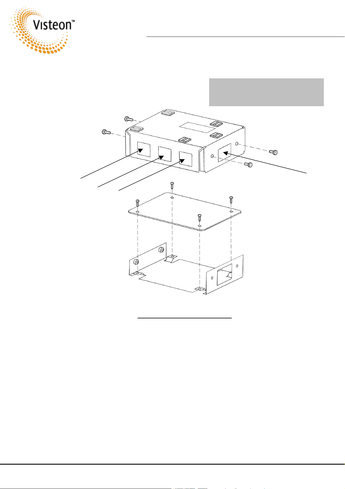
Figure 1 Control Module Housing
Figure 1 Control Module Housing
Figure 1 Control Module HousingFigure 1 Control Module Housing
1. Loosen screws 1 to 4 and remove the control box lid.
2. Remove screws 5 to 8. and separate the PCB from the control box base.
3. Visually inspect the components for obvious signs of mechanical or electrical damage.
4. Proceed to section C.
30-900-00015 Issued 2002-11-28 Page 3 of 19 © Copyright Visteon 2002
Page 4
Service Manual – Renault System
C. Diagnosis and Repair.
1. Connect the open control module to the test kit.
2. Connect the 12.5 V power supplies to the test kit.
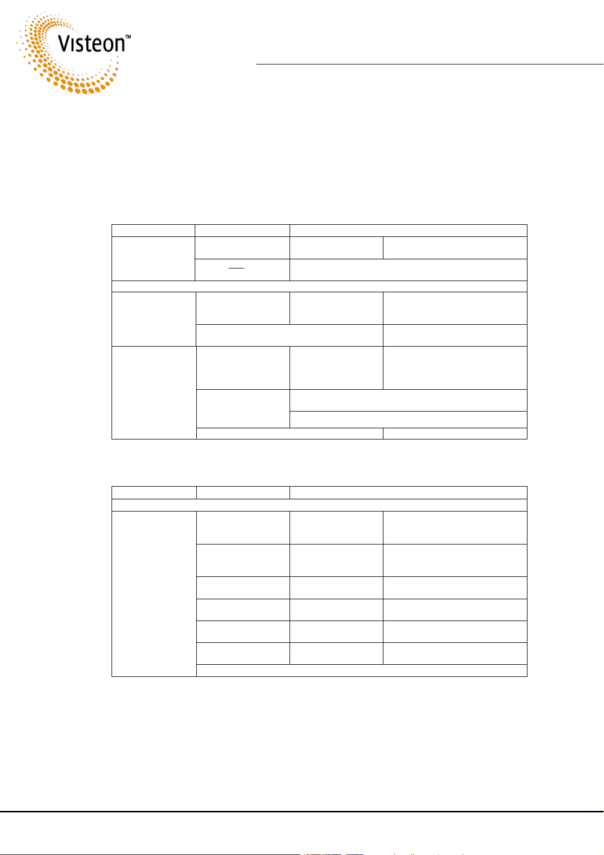
3. Compare the symptoms observed under A. Initial Inspection and Test with the symptoms
listed below to locate the components likely to be faulty and effect the necessary repairs.
Symptom
Symptom Investigation
SymptomSymptom
as DVD or TV
missing from OSD
Menu
Media Device
Switching OFF/ON
continuously,
video signal
present
Audio Fault
No sound both
left and right
Symptom
Symptom Investigation
SymptomSymptom
Power Faults
Power Faults
Power FaultsPower Faults
No Power / No
LCD
Investigation Corrective Action
InvestigationInvestigation
Check for <1 V at IC1
Corrective Action
Corrective ActionCorrective Action
If OK go to next line Replace IC1. Media device such
pin11,12
Power OFF
supply for
Repower system and recheck fault.
5 Seconds
Check for <0.5 V
TR3 collector
If OK go to next line Check TR3, D1, IC1, C3, C26,
C36, C37 in turn. Replace faulty
components.
IC11 defective Replace IC 11.
Check Audio route in
If OK go to next line Replace faulty components.
logical manner
IC7/19 > IC1 >
IC2/5 > IC3/4
Video OK?
Check as No Colour / poor /no image – NO audio OSD OK
– See "Image Faults" below.
If OK go to next line.
Check IC1, IC3, IC4.defect - Replace defective components.
Investigation Corrective Action
InvestigationInvestigation
Corrective Action
Corrective ActionCorrective Action
Check 12 V on F1 If OK go to next line F1 Defect - check for S/C on
output. Replace defective
components.
Check 5 V/12 V IC
17
If OK go to next line IC 17/D3 Defective or S/C on
output. Replace defective
components.
Check IR sig. on
IC11 pin 8
Check Xtal sig. on IC
11pin 6, 7
Check < 0.6 V IC
11tPin 2
If OK go to next line Check IC12/13/14. Replace
defective components.
If OK go to next line XTAL or IC11 Defect. Replace
defective components.
If OK go to next line TR6 defect IC11 Defect. Replace
defective components.
Check 5 V IC 16 Pin 2 If OK go to next line TR6 defect, IC16. Replace
defective components.
Check for PCB damaged pins . Replace defective components.
30-900-00015 Issued 2002-11-28 Page 4 of 19 © Copyright Visteon 2002
Page 5
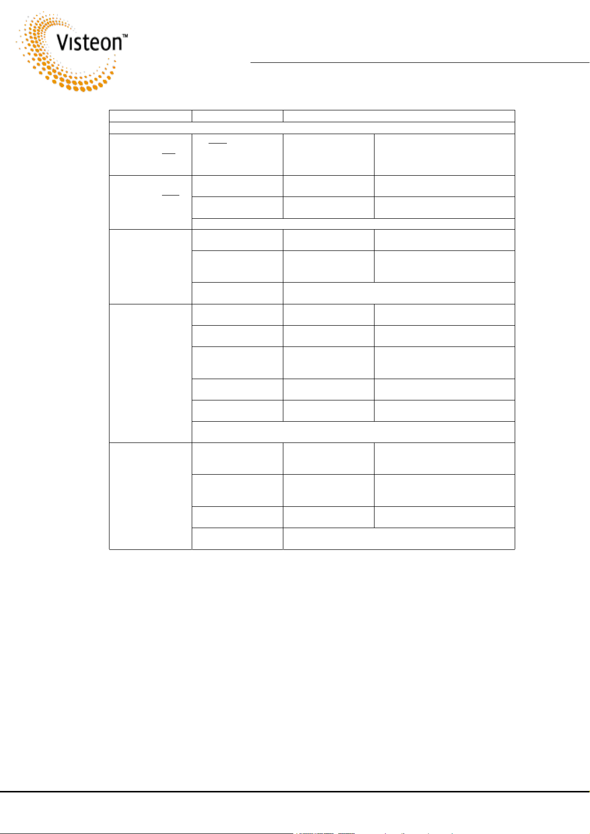
Symptom
Symptom Investigation
SymptomSymptom
Image Faults
Image Faults
Image FaultsImage Faults
LCDs on.
No OSD on one
Investigation Corrective Action
InvestigationInvestigation
Is color
image shown
on LCD?
LCD
LCDs on.
No OSD on both
LCDs
Check Waveform
IC11 Pin 9,10
Check Waveform
IC8, 9 Pin 7
CN4 damaged - Check For PCB Damage. -Replace defective components.
No colour, poor
/no image – No
audio, OSD OK
Check Waveform IC1
pin 1/8
Check 9V IC18 pin 3 If OK go to next line IC18 Defect - check for S/C on
Check Waveform IC1
pin 33/34
No colour, poor
Is OSD OK? If OK go to next line Go to image Faults – No OSD
/no image – audio
OK:
All 3 Inputs, one
or both LCDs
Check Waveform IC1
pin 1,8,15
Check Waveform IC1
pin 44,53
Check Waveform
IC10 pin 7,8
Check Waveform
CN4 pin 8/18
Check Correct Values R35/36 - Reg supplies 5/12/Gnd.
Service Manual – Renault System
Corrective Action
Corrective ActionCorrective Action
If yes go to next line TR1/2, IC8 Defective CN4
damaged. Replace defective
components.
If OK go to next line IC11 Defect - eeprom corrupt.
Replace defective components.
If OK go to next line IC 8/9 Defect. Replace defective
components.
If OK go to next line CN1/2 / test Media / looms.
Replace defective components.
O/P. Replace defective
components.
If OK suspect Defective IC / inspect soldering or PCB
damage. Replace defective components.
above.
If OK go to next line IC v / defect IC1 x S/C. Replace
defective components.
If OK go to next line Defect IC1, C26/36/37-PCB
O/C. Replace defective
components.
If OK go to next line IC10 Defect Replace defective
component.
If OK go to next line R35, 36 – PCB Defect. Replace
defective components.
No colour, poor
/no image – audio
OK.
One input, both
LCDs
Check Waveform
CN1/2/3 pin7
If OK go to next line Check connector / test
Media/looms. Replace defective
components.
Check Waveform IC1
pin 44, 53
If OK go to next line Defect IC1, C26/36/37-PCB
O/C. Replace defective
components.
Check Waveform
If OK go to next line Recheck Fault symptoms
IC10 7, 8
Check test looms Check Reg supplies 5/9/12/Gnd. Replace defective
components.
30-900-00015 Issued 2002-11-28 Page 5 of 19 © Copyright Visteon 2002
Page 6
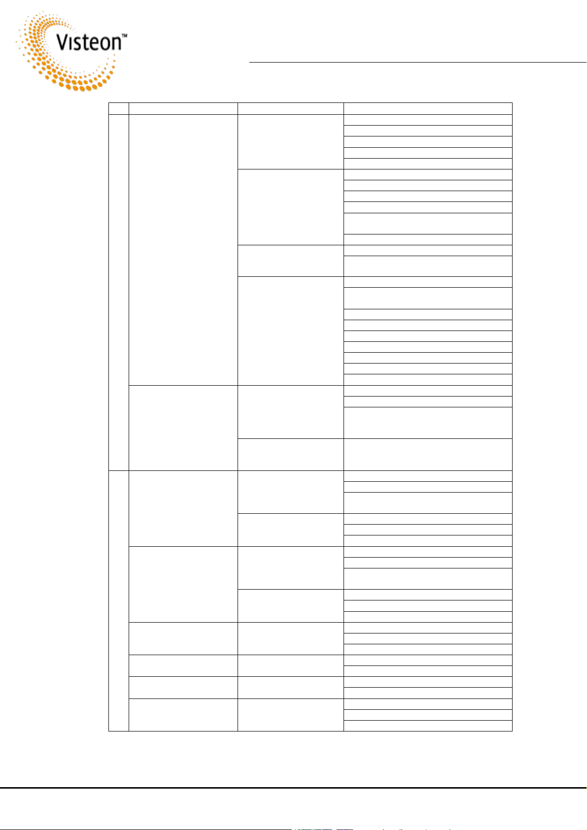
Symptom
Symptom Possible Cause
SymptomSymptom
Possible Cause Probable Diagnosis
Possible CausePossible Cause
Micro defective.
Power supply circuit not
PPPP
switched on
oooo
wwww
Control Module Power
eeee
Failure.
rrrr
interface board IR sensor
missing
CCCC
oooo
nnnn
tttt
IR detection circuit
failure.
rrrr
oooo
llll
Micro does not detect
that the media1 or media
Control module fails to
detect media device
No video on left screen,
audio OK
VVVV
No video on right screen,
audio is ok
iiii
dddd
eeee
oooo
Poor quality video on left
and right screens, audio
OK
right screen, audio OK
screen, audio OK
No video picture, on
either screen, DVD
controls working
2 sense lines are
grounded
Micro does not detect
either Media1 or media 2
sense lines
No video output from
IC1 circuit area
No video output from
IC10 circuit area
No video output from
IC1 circuit area
No video output from
IC10 circuit area
Video input signal not
terminated properly.
Video output signal not
terminated properly
Video output signal not
terminated properly
No IIC clock signal to
LCD screens
Service Manual – Renault System
Probable Diagnosis
Probable DiagnosisProbable Diagnosis
IC11 micro crashed
XT1 inoperative
TR5 collector output failed low (reset).
D3 failed o/c.
IC 17 (5 V)
TR5 failed low
IC16 switch inoperative
TR6 output failed low
Dry joint at IC11 pin 2.
Dry joint or broken track between IC16
pin 23 and TR6 collector.
D2 failed s/c
R55 & R56 o/c or missing +5 V supply to LCD
C77 & C76 s/c to gnd.
IC12 internally defective holding 14 high.
CN3 pin 3 or CN4 PIN 4 or CN4 pin14
gnd.
C94 s/c to gnd
LK1 missing (no +5V)
R42 missing
IC14 faulty
C50 s/c to gnd
IC13 faulty
R59, R48 OR R49 o/c.
R63 or R54 o/c
IC11 pin 11 or 12 dry-jointed
Poor continuity between
CN1 pin 2 and IC11 pin 12 and CN2
pin 2 and IC11 pin 11
Media device connected after turning on
power supply to the control box.
C11 or C12 or C13 o/c
IC1 defective
Dry or open joints on IC1 video input pins
1, 8, & 15 or output pins 44 & 53.
C45, C48, R36, L9 o/c
IC10 defective
Dry/ open joints on IC10 pins
C11. C12, C13 o/c
IC1 defective
Dry open joints on IC1 video input pins 1,
8 & 15 or output pins 53 & 44.
C44, C47, R35, L8 o/c
IC10 defective
Dry/ open joints on IC10 pins
R1, R2, R3 dry joint/ o/c
RV1 or RV2 or RV3 partial short
C11, C12, C13 o/c
C44, C47, R35 o/c or dry joint Poor quality video on
RV18 partial short
C45, C48, R36 o/c or dry joint Poor quality video on left
RV15 partial short
C80 s/c to gnd.
IC9 pin 7 failed, open
R31 open, dry-jointed
30-900-00015 Issued 2002-11-28 Page 6 of 19 © Copyright Visteon 2002
Page 7
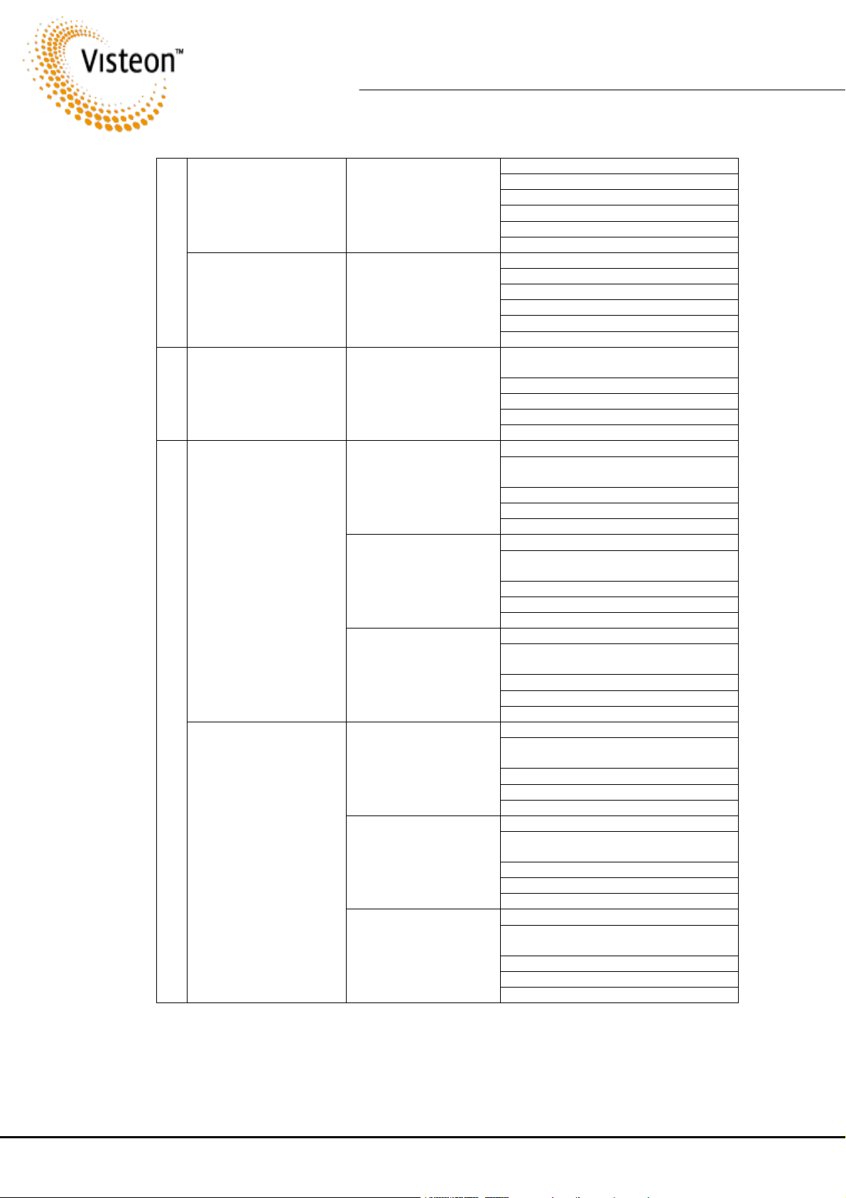
Service Manual – Renault System
C78 s/c to gnd
Loss of control of OSD
functions e.g. contrast,
colour, etc. . on right
screen.
OOOO
SSSS
DDDD
Loss of control of OSD
functions e.g. contrast,
colour, etc. on left screen
DDDD
DVD player does not
VVVV
respond to remote control
DDDD
Left side audio missing or
out of spec, video OK: left
and/or right screen
AAAA
uuuu
dddd
iiii
oooo
Right side audio missing or
out of spec, video OK: left
and/or right screen
IIC control signals to
right LCD screen
defective
IIC control signals to left
LCD screen defective
IR signal not being
relayed from the control
module
Failure of any left-side
audio input circuit
associated with CN1
Failure of any left-side
audio input circuit
associated with CN2
Failure of any left-side
audio input circuit
associated with CN3
Failure of any right-side
audio input circuit
associated with CN1
Failure of any right-side
audio input circuit
associated with CN2
Failure of any right-side
audio input circuit
associated with CN3
IC8 pin2 failed, open
IC9 pin 7 to CN4 pin 2 open, dry-jointed
IC11 pin 16 output failed, open
R28 open, dry-jointed
TR1 failed, open
C79 s/c to gnd
IC8 pin7 failed, open
IC9 pin7 to CN4 pin12 open, dry-jointed.
IC11 pin 14 output failed or open
R29 open, dry-jointed
TR2 failed, open
IC11 pin19 open, dry jointed, output
failed
R57 open, dry jointed
D5 failed s/c to gnd or to 5 V
L2 open, dry-jointed
CN1 pin5 dry-jointed
C5, C82 o/c or dry joint
R4 terminator, R10, R75, R77 o/c or dry
joint,
IC7 failed or not receiving 9 V supply
IC1 partially defective
Dry joint on IC1 pin 43 or 52.
C6, C86 o/c or dry joint
R5 terminator, R11, R80, R83, o/c or dry
joint
IC7 failed or not receiving 9 V supply
IC1 partially defective
Dry joint on IC1 pin 43 or 52.
C7, C88, o/c or dry joint
R6 terminator, R12, R86, R87, o/c or dry
joint,
IC19 failed or not receiving 9 V supply
IC1 partially defective
Dry joint on IC1 pin 43 or 52
C8, C83 o/c or dry joint
R7 terminator, R13, R78, R84 o/c or dry
joint,
IC7 failed or not receiving 9 V supply
IC1 partially defective
Dry joint on IC1 pin 45 or 54
C9, C85 o/c or dry joint
R8 terminator, R14, R81, R83 o/c or dry
joint
IC7 failed or not receiving 9 V supply
IC1 partially defective
Dry joint on IC1 pin 43 or 52
C10, C87, o/c or dry joint
R9 terminator, R15, R83, R85, R88, o/c
or dry joint
IC19 failed or not receiving 9 V supply
IC1 partially defective
Dry joint on IC1 pin 43 or 52
30-900-00015 Issued 2002-11-28 Page 7 of 19 © Copyright Visteon 2002
Page 8
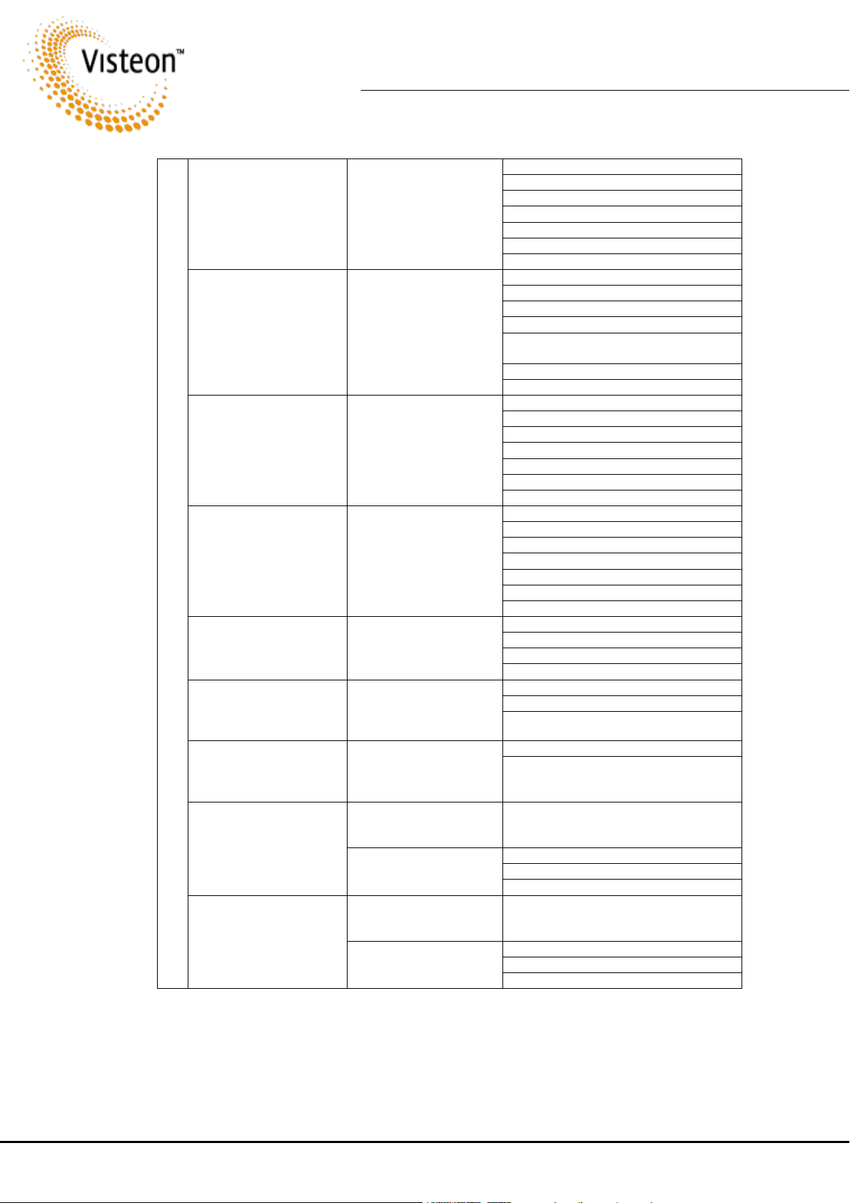
Service Manual – Renault System
C25, C29 or C35 o/c
C32 failed s/c
IC4 pin 7 open
IC4 partially defective
IC5 pin 2, 12, 13 or 19 open (no IIC)
IC5 partially defective
R26 or R20 o/c
C24, C31 or C34 o/c
C33 failed s/c
IC4 pin 6 open
IC4 partially defective
IC5 pin 1, 12, 13 or 18, open
(no IIC)
IC5 partially defective
R21 or R27 o/c
C16, C18 or C20 o/c
C22 failed s/c
IC2 pin 2, 12, 13 or19 open (no IIC)
IC2 partially defective
IC3 pin 7 open
IC3 partially defective
R16 or R24 o/c
C15, C19 or C21 o/c
C23 failed s/c
IC2 pin 1, 12, 13, 18, open (no IIC)
IC2 partially defective
IC3 pin 6, open
IC3 partially defective
R17, R25 o/c
IC11 pin3 open, dry jointed, output failed
IC19 pin 9 output failed
LK4 defective
TR7 defective
IC11 pin3 output failed high
R102 defective
TR7 failed high (>6 V)
IC11 pin3 output failed low Right screen audio not
TR7 failed o/c
IC2 pin12 and/or 13 open.
C28 open
IC2 pin 15 open (no 9 V)
IC2 is defective
IC5 pin 12 and/or 13 open
C30 open
IC5 pin15 open (no 9 V)
IC5 defective
Left side audio on left
screen missing or out of
spec., video OK.
Right side audio on left
screen missing or out of
spec., video OK.
Left side audio on right
screen missing
AAAA
Right side audio on right
uuuu
screen missing
dddd
iiii
oooo
Audio signal not reaching
rear shelf speakers
(headphones OK)
Left screen audio not
reaching rear shelf
speakers (headphones,
right screen audio OK)
reaching rear shelf
speakers (headphones,
right screen audio OK)
Unable to adjust audio
controls: treble, bass etc.
on right screen. OSD OK.
Unable to adjust audio
controls: treble, bass etc.
on left screen. OSD OK.
Failure in left side audio
processing within the left
screen audio
processor/amplifier
circuit
Failure in right side audio
processing within the left
screen audio
processor/amplifier
circuit
Failure in left side audio
processing within the
right screen audio
processor/amplifier
circuit
Failure in right side audio
processing within the
right screen audio
processor/amplifier
circuit
Channel select signal not
being relayed from
control module
Channel select signal for
left screen audio not
being relayed from
control module
Channel select signal for
right screen audio not
being relayed from
control module
No IIC clock signal to
right audio processor
chip
Right screen audio
processor IC2 not
working
No IIC clock signal to
right audio processor
chip
Left screen audio
processor IC5 not
working
4. Complete repairs to the control module. Ensure that the repaired items are clean.
5. Reassemble the control module by performing the dismantling procedure described above
in reverse.
6. Retest the module as described in section A-3
30-900-00015 Issued 2002-11-28 Page 8 of 19 © Copyright Visteon 2002
Page 9

Service Manual – Renault System
D. Reference
General Description:
General Description:
General Description:General Description:
The control module is central to the Entertainment system. It interprets and implements
commands entered by the user using the system's infrared remote control. These
commands are relayed to the control module via the system's infrared sensors mounted in
the screen modules. It also distributes power to the system and detects the vehicle's
ignition state via a sense wire running from CN1 to the vehicle's ignition switch. This
enables it to limit battery drain whilst the vehicle is not in use.
The control module receives audio and video inputs from the DVD Player via connector
CN1 and from the vehicle's TV tuner (if fitted) via connector CN2. It is also able to receive
a further audio/video input and supply a low-level two-channel audio output via CN3.
Technical Description:
Technical Description:
Technical Description:Technical Description:
A micro-controller in the Control Module supplies and controls the power to the system via
2
an I
C bus. On receipt of a
simple system check and then sends commands to other parts of the system to bring them
on line.
power-on
command from the Infrared Controller it performs a
When a screen has been selected using the infrared remote control the Control Module
identifies the selected screen and displays on it a menu providing the user with access to
the functions detailed below:
• Independent switching of three Audio-Visual inputs (DVD, TV and AUX)
• Video manipulation (Colour, brightness, contrast and aspect ratio of the display.)
• Audio processor (Bass, Treble and Volume)
• On-Screen instructions language selection
• Switch on/off individual screen displays
The Control Module also determines which media source has been routed to the selected
screen and relays commands in the appropriate protocol.
For example if, while Screen A is displaying the DVD transmission, an infrared play
command is detected at screen A, it would be captured, stored and relayed to the DVD in
the DVD's Infrared protocol. If screen B is displaying a TV transmission the play command
would be transmitted in the vehicle's TV tuner infrared protocol.
A non-volatile memory stores the display instruction language in use and the current Audio
and Video settings for each output channel. These settings are reloaded on power-up with
the exception of the audio volume level, which defaults to a low state.
Support equipment that has been powered off is detected by the lack of video sync pulse.
This can be caused by auto shutdown after extended pause mode. When this happens the
module responds by transmitting a power-on command to the support equipment until it is
ready to accept it and power up. The supply of the video sync pulse then resumes and the
module stops transmitting the power-on command.
30-900-00015 Issued 2002-11-28 Page 9 of 19 © Copyright Visteon 2002
Page 10
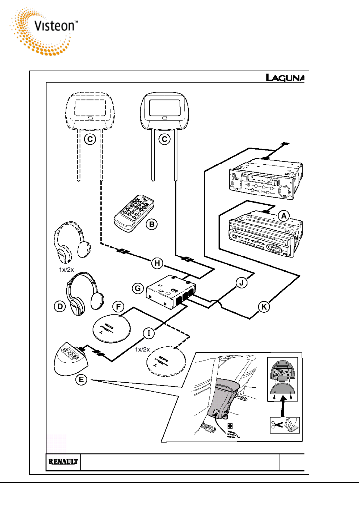
Con
Connection Diagram
nection Diagram
ConCon
nection Diagramnection Diagram
Service Manual – Renault System
30-900-00015 Issued 2002-11-28 Page 10 of 19 © Copyright Visteon 2002
Page 11
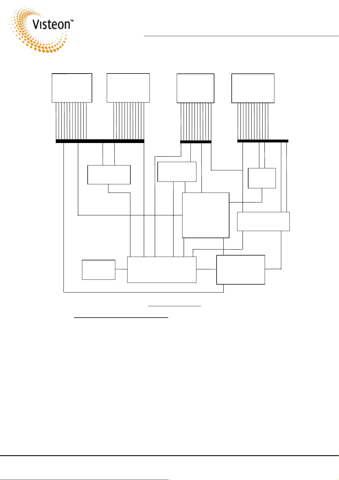
Service Manual – Renault System
CN 1
DVD
CN 2
CN3
Auxiliary Panel
CN4
Video Output
to TFT Screens
Audio
I2C Bus Extender
Processors
Audio
Processors
Video/Audio
EPROM
Analogue Audio and Video signals:
Analogue Audio and Video signals:
Analogue Audio and Video signals:Analogue Audio and Video signals:
Microprocessor
Functional Diagram
Functional Diagram
Functional DiagramFunctional Diagram
Switch
Power supply
I2C Bus Extender
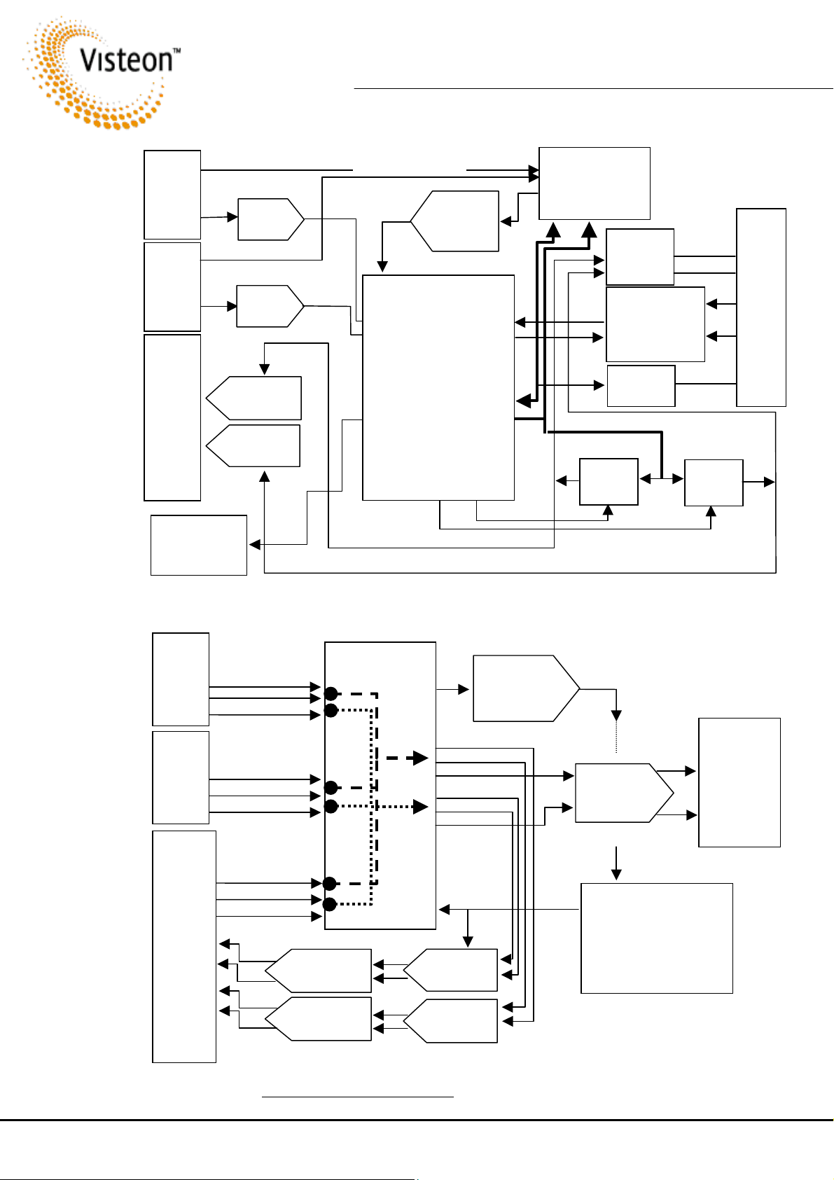
Quad OP amps IC7 & 19 (if fitted) are used to reduce any ground noise from the Vehicle
by employing a “Floating” audio ground that is referenced from the media devices ground.
Audio signals from these devices along with the corresponding CVBS signals are applied to
²
IC1 (I
C controlled AV Switch matrix). Audio signals are routed through this device to the
relevant audio processors IC2/5 and then on to the Headphone amplifiers IC3/4
Video signals from IC1 are buffered by IC10 and supplied to the relevant LCD module.
30-900-00015 Issued 2002-11-28 Page 11 of 19 © Copyright Visteon 2002
Page 12
k
k
k
k
CN1
CN1
CN1CN1
VCR
VCR
VCRVCR
5
CN2
CN2
CN2CN2
DVD
DVD
DVDDVD
5
CN3
CN3
CN3CN3
HP1
HP2
VCR Detect
Audio Amp
DVD Detect
Audio Amp
IC2
IC2-Audio
IC2IC2
Processor
IC5
IC5-Audio
IC5IC5
Processor
Service Manual – Renault System
VIDEO/AU
D1/TR3
VIDEO
DETECT
17
19 1,20
18 8
LOGIC CONTROL
IC11
IC11
IC11 IC11
CLK10
2 PWR EN SDA-9
IIC BUS
EN1 EN2
14 16
IC1
37
33 34
IC8
IC8
IC8IC8
3 SDA1
IC12, 13, 14
IC12, 13, 14
IC12, 13, 14IC12, 13, 14
IR
Sis-Strength
/Selector
IC9
IC9
IC9IC9
6 SCL
TR1
TR1
TR1TR1
SDA1
TR2
TR2
TR2TR2
SDA2
CN4
CN4
CN4CN4
1
11
4
14
2,12
PSU
IC16
IC16
IC16 IC16
CN1
DVD
Video
R
L
CN2
TV
Video
R
L
CN3
AUX
Video
R
L
Control Signal Bloc
Control Signal Bloc
Control Signal Bloc
Control Signal Bloc
IC1
AV Switching
D1/TR3
VIDEO SIG
DETECT
CN4
Screen1
IC10
VIDEO AMP
Screen2
LOGIC CONTROL
R1 HP
L1 HP
IC3-Screen 1
Audio Amp
IC2-Audio
Processor
R2 HP
L2 HP
IC4-Screen 2
Audio Amp
Router Signal Block Diagram
Router Signal Block Diagram
Router Signal Block DiagramRouter Signal Block Diagram
IC5-Audio
Processor
30-900-00015 Issued 2002-11-28 Page 12 of 19 © Copyright Visteon 2002
Page 13
Service Manual – Renault System
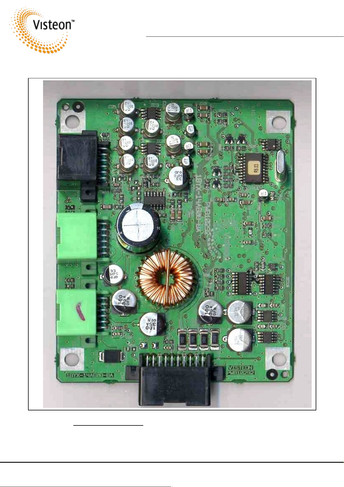
Control Module pcb Top
Control Module pcb Top
Control Module pcb TopControl Module pcb Top
30-900-00015 Issued 2002-11-28 Page 13 of 19 © Copyright Visteon 2002
Page 14
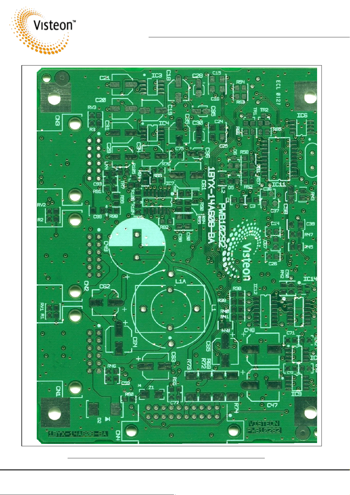
Service Manual – Renault System
Top View of the Control Module pcb Detailing Circuit Reference Nos.
Top View of the Control Module pcb Detailing Circuit Reference Nos.
Top View of the Control Module pcb Detailing Circuit Reference Nos.Top View of the Control Module pcb Detailing Circuit Reference Nos.
30-900-00015 Issued 2002-11-28 Page 14 of 19 © Copyright Visteon 2002
Page 15
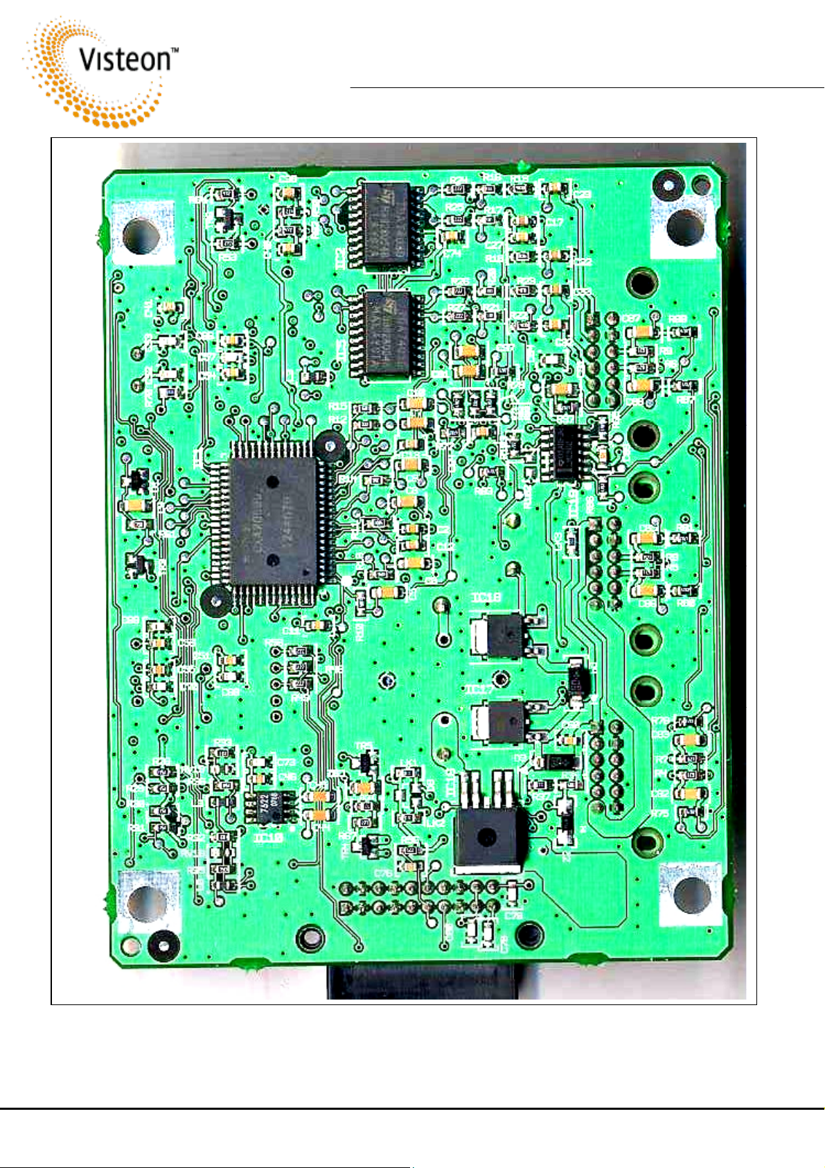
Service Manual – Renault System
Control Module pcb Bottom
Control Module pcb Bottom
Control Module pcb BottomControl Module pcb Bottom
30-900-00015 Issued 2002-11-28 Page 15 of 19 © Copyright Visteon 2002
Page 16
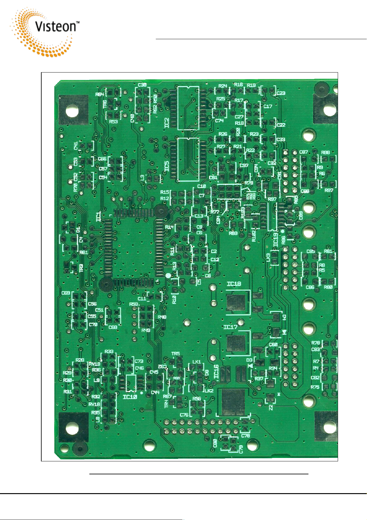
Service Manual – Renault System
Bottom View of the Control Module PCB Detailing Circuit Reference Nos.
Bottom View of the Control Module PCB Detailing Circuit Reference Nos.
Bottom View of the Control Module PCB Detailing Circuit Reference Nos.Bottom View of the Control Module PCB Detailing Circuit Reference Nos.
30-900-00015 Issued 2002-11-28 Page 16 of 19 © Copyright Visteon 2002
Page 17
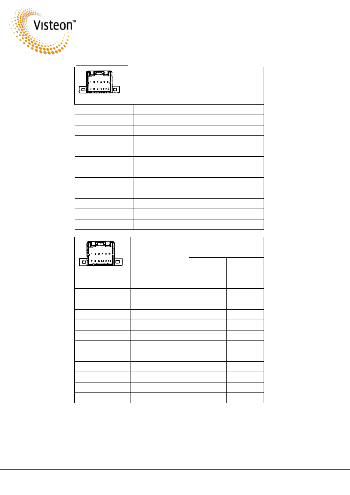
Connector Details
Connector Details
Connector DetailsConnector Details
CN 1 DVD
CN 1 DVD
CN 1 DVDCN 1 DVD
Service Manual – Renault System
Circuit Function
Circuit Function To
Circuit FunctionCircuit Function
To
ToTo
1 Not used Not used
2 Infrared Gnd DVD
3 DVD enable DVD
4 Not used Not used
5 Infrared + DVD
6 Not used Not used
7 Video + DVD
8 Video Gnd DVD
9 Audio R+ DVD
10 Audio L+ DVD
11 Audio ground DVD
12 Ground Belden 9539
To
To
ToTo
Function
Function
FunctionFunction
CN
CN2
CNCN
1 Accessory Radio Ignition ?
2 Infra Red- ? ?
3 Not used Not used Not used
4 Not used Not used Not used
5 Not used Not used Not used
6 Main Power + 12 V Battery ?
7 Not used Not used Not used
8 Not used Not used Not used
9 Not used Not used Not used
Laguna
Laguna
LagunaLaguna
Espace
Espace
EspaceEspace
Scenic
Scenic
ScenicScenic
10 Not used Not used Not used
11 Not used Not used Not used
12 Power ground ? ?
30-900-00015 Issued 2002-11-28 Page 17 of 19 © Copyright Visteon 2002
Page 18
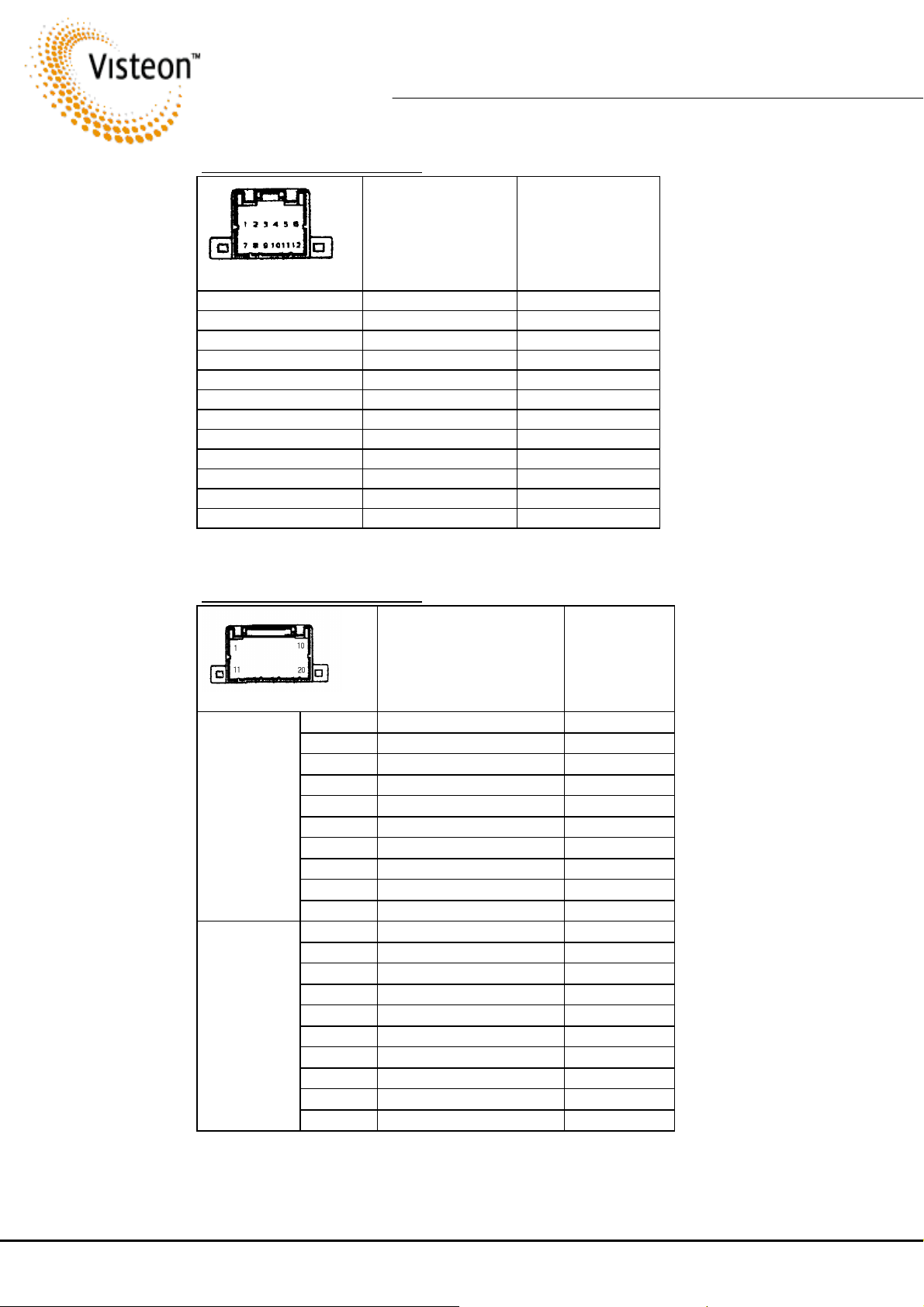
Connector Details Continued
Connector Details Continued
Connector Details ContinuedConnector Details Continued
CN3 Aux Panel
CN3 Aux Panel
CN3 Aux PanelCN3 Aux Panel
Service Manual – Renault System
Function
Function To
FunctionFunction
To
ToTo
1 Audio R out Ch1 Aux Panel
2 Audio L out Ch1 Aux Panel
3 Not used Not used
4 Audio out R Ch2 Aux Panel
5 Audio out L Ch2 Aux Panel
6 Power Out Aux Panel
7 Video + in Aux Panel
8 Video ground Aux Panel
9 Audio in R Aux Panel
10 Audio in L Aux Panel
11 Audio ground Aux Panel
12 Ground Aux Panel
Connector Details Continued
Connector Details Continued
Connector Details ContinuedConnector Details Continued
CN4 TFT Screens
CN4 TFT Screens
CN4 TFT ScreensCN4 TFT Screens
Section
1
Section
2
Function
Function To
FunctionFunction
To
ToTo
1 XSDA I2C data bus CN 5-1
2 XSCL Sync Clock I2C CN 5-2
3 Ground/Screen CN 5-3
4 Infrared Sense in CN 5-4
5 5 V IR supply out CN 5-5
6 LCD Power +12 V CN 5-6
7 Video Out CN 5-7
8 LCD Video gnd CN 5-8
9 Backlight Ground CN 5-9
10 Backlight +12 V CN 5-10
11 XSDA IIC data bus CN 15-1
12 XSCL Sync Clock IIC CN 15-2
13 Ground/Screen CN 15-3
14 Infrared Sense in CN 15-4
15 5 V IR supply out CN 15-5
16 LCD Power +12 V CN 15-6
17 Video Out CN 15-7
18 LCD Video gnd CN 15-8
19 Backlight Ground CN 15-9
20 Backlight +12 V CN 15-10
30-900-00015 Issued 2002-11-28 Page 18 of 19 © Copyright Visteon 2002
Page 19
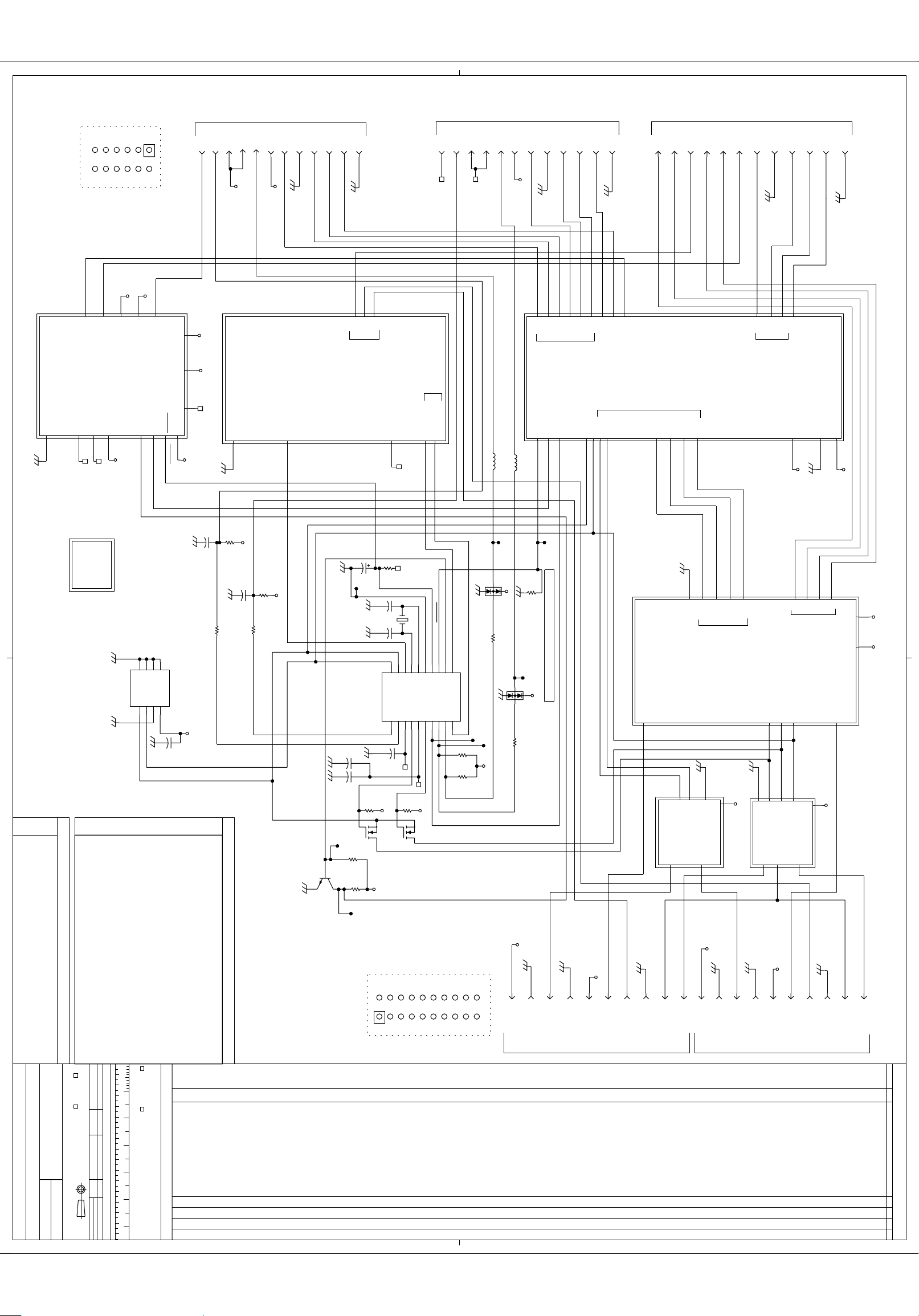
PWB Bottomside View
of CN1,CN2 & CN3
(REF. SHEET 4)
POWER_SUPPLY BLOCK
POWER_SUPPLY
GND
GND
Pin6
Pin12
VOLVO_AUDIO_SEL_DRIVE
ACC_VIA_DIODE
VOLVO_AUDIO_SEL_DRIVE
ACC_VIA_DIODE
+5V_VIA_D8
+5V_BATTF
VCC
+5V_VIA_D8
+5V_BATTF
VCC
VBAT
TO JVC VCR OR NECVOX DVD TO (TBE) DVD
Pin1
Pin7
SBATT
VBAT
ACC
SBATT
VFILTER
+9VA
POWERSW
+5V_ACC
ISENSE
RESET
ISENSE
RESET
POWERSW
VCC
-1CN1
ACC
VFILTER
+9VA
+5V_ACC
+5V
+5V
-2CN1
VCR_SENSE
IR_INTERFACE
4 CN1-5 CN1
3 CN1
-
-
VCR_REMOTE_CTRL
SBATT
GND
GND
-8CN1
-9CN1
-10CN1
-11CN1
-7CN1
-6CN1
RIN1V1LIN1
GND
VBAT
(REF. SHEET 3)
IR_INTERFACE BLOCK
INT1
INT1
-12CN1
AUDIO1_GND
GND
IR0
IR0
INPUTS
IR2
IR1
IR1
IR2
+5V_VIA_D8
+5V_VIA_D8
OUTPUTS
-1CN2
IR_STATUS0
IR_STATUS1
IR_STATUS0
IR_STATUS1
ACC
-2CN2
DVD_SENSE
DVD_SENSE
IR2
-3 CN2
IR1
4 CN2
-
SBATT
VCR_SENSE
VCR_REMOTE_CTRL
5 CN2
-
-6CN2
DVD_REMOTE_CTRL
DVD_REMOTE_CTRL
L2
L3
-7CN2
V2
VBAT
V1
VOLVO_AUDIO_SELECT
AV_SWITCH
VOLVO_AUDIO_SELECT
-8CN2
GND
RIN1
ISENSE
ISENSE
-9CN2
LIN1
INPUTS
9VSENSE
9VSENSE
RIN2
-10CN2
-11CN2
-12CN2
AUDIO2_GND
LIN2
GND
AUDIO1_GND
AUDIO2_GND
LIN2
RIN2
V2
SDA
VOUT2
SCL
VOLVO_AUDIO_SEL_DRIVE
VOUT1
1 CN3
R1
VOLVO_AUDIO_SEL_DRIVE
OUTPUTS
ROUT2
LOUT2
2 CN3
3CN3
IR0
L1
LOUT1
ROUT1
TO AUXILLIARY PANEL
6 CN3
5 CN3
4 CN3
7CN3
ACC_VIA_DIODE
R2
L2
(REF. SHEET 2)
V3
AV_SWITCH BLOCK
INPUTS
12CN3
11CN3
10CN3
9CN3
8CN3
V3
GND
LIN3
RIN3
+5V
RIN3
AUDIO3_GND
+5V
+5V
LIN3
AUDIO3_GND
GND
GND
+9VA
GND
R1L1R2
(Output Signal)
(Output Signal)
+9VA
L2
(Output Signal)
(Output Signal)
MECH_DETAIL_TOP
1. R51, R52, R65 & R66 NOT FITTED.
OTHER NOTES:
ENFIELD
MECH
NM24C16UEM8
10. All GROUNDS(GNDS, GNDVOUT..etc) shall be made a
11. Refer to SHEET4 for TRACK CURRENTS.
9. Introduce GUARD GND tracks between audio,video & IR sigs
and other adjacent signal tracks.
SINGLE GROUND PLANE.
Tracks affected are LIN1&2, RIN1&2, L1&2, R1&2
LOUT1&2, ROUT1&2 and also IR0,1 and 2.
4.7K5%R62
470N
10%
C40
470N
10%
R63
5%
220
5%
321
A0A1A2
VSS SDA
IC6
SCLNCVCC
876
54
100N
10%
C41
5. Starpoint the +5V lines from the BULK
6. Place all decoupling caps near power pins of ICs.
7. Ensure that no components are present under the
8. COMMON all types of GND (GNDS etc..) onto a SINGLE
GROUND PLANE.
the L1 or L1a components.
footprint of L1 or L1a (see POWER_SUPPLY BLOCK)
capacitor C64.
or within a clearance gap of 0.03 inches around
and other adjacent signal tracks.
VCR_SENSE_TO_MICRO
+5V
SCL
SDA
3. Place XT1 near IC11.
4. Introduce GUARD GND tracks between SCL,SDA
1. Ensure IC11 is provided with an MGP.
2. Place C66,C54,C57,C52,C53,R70 close to IC11
and with their GND points tied to the MGP.
Ensure that these GND points are directly
connected to the MGP; not via GND loop branches.
EMC NOTES:
+5V
4.7K5%R50
C38
R54
220
DVD_SENSE_TO_MICRO
SDA
LOUT2
LOUT1
ROUT1
ROUT2
MCB1000_TOP_LEVEL_SCHEMATIC
+5V
+9VA
XSDA1
Temporary
Pin num:
PWB
CN4-1
Pin num:
Actual
IR_STATUS1
1.2K
5%
TP86
TP85
Pin20
Pin10
TP44
+5V
D5
200MA
70V
BAV99
R57
D6
+5V
1CN4
CN4-20
C58
20%
10U
16V
+5V_BATTF
INT1
SDA
SCL
+5V
SDA
SCL
MICRO_POWERSW_CTRL
SCL
C575%10P
100N
10%
C54
SDA
TP60
45V
225MW
BC817-25
500MA
TR6
8.2K5%R43
15P5%C52
RESON,XTAL,6.29MHZ,HC-49/U-S
15P5%C53
10
10 11
8
9
INT1
SDA
SCL
87LPC764
P1.1
P0.7
P1.0
11
13
129
138
12
+5V_ACC
C66
10%
100N
4.7K
5%
4.7K5%R64
2.7K5%R53TP63
(VIA)
TP59
PWB Bottomside View
Pin11
of CN4
Pin1
4.7K
R65
5%
+5V
BSS138
220MA
TR2
+5V
XT1
714
7
5
RST3P1.62P1.7
X2
X16VSS
P0.4
P0.6
P0.5
VDD
15
14
16
+5V_BATTF
R66
+5V
BSS138
220MA
TR1
IR_STATUS0
MICRO_POWERSW_CTRL
VOLVO_AUDIO_SELECT
RESET
4
23456
1
1
P0.0
P0.119P0.2
P0.3
17
20
181920
171615
18
5%
5%
9VSENSE
4.7K
4.7K
IC11
R51
R52
TP62 NOTE: R70 NOT FITTED FOR VOLVO!
R70
0
TP45
+5V
200MA
70V
BAV99
5%
1.2K
R58
SDA1
SDA2
VFILTER
VIDEO_OUT2
GND
2 CN4
-
3CN4
CN4-19
CN4-18
9VSENSE
POWERSW
CN4-17
GND
GND
ROUT2
INPUTS
VOUT2
VOUT1
IR1
IR2
AUDIO_VIDEO_OUTPUT
SEL2
GND
VOUT1
VOUT2
GND
VOUT1
VOUT2
VIDEO_OUT2
VIDEO_BUFFER
VFILTER
SEL2
IR2
7 CN4-8 CN4
-
CN4-14
GND
CN4-13
GND
4 CN4
-
5CN4-6CN4
CN4-16
CN4-15
VIDEO_OUT1
XSCL
XSDA2
9CN4-10CN4-11CN4
CN4-12
CN4-11
CN4-10
LOUT2
VCC
VIDEO_BUFFER
VFILTER
GND
12 CN4
-
CN4-9
LOUT1
ROUT1
VCC
REF SHEET 7
I2C_BUFFER
VIDEO_OUT1
13CN4
CN4-8
(REF. SHEET 5)
AUDIO_OUTPUT
SDA1
SDA2
GND
GND
SDA1
SDA2
XSDA2
XSCL
VFILTER
GND
14 CN4
-
15CN4-16CN4
CN4-7
CN4-6
R1
R1
OUTPUTS
SCL
SCL
+5V
XSDA1
SEL1
CN4-5
R2
L1
L1
R2
I2C_BUFFER
REF SHEET 6
IR1
17 CN4-18 CN4
-
CN4-4
GND
CN4-3
L2
L2
SEL1
+5V
+5V
+9VA
XSCL
19CN4-20CN4
CN4-2
MATERIAL
NAME
NO.
MS-XXXX-3458-XX
PWB_NUMBER=10292
SKETCH - WIRING DIAGRAM
DRAWING_NAME
PLANT CODE:
DATE
APP
PLANT_CODE
POWERVIEW
UNLESS OTHERWISE SPECIFIED:
DIMENSIONS ARE IN
ANGULAR DIM. +/-
MACHINED DIM. +/-
INCHES
MILLIMETERS
STAMPED DIM. +/-
3RD ANGLE PROJECTION
METRIC20 30 40 50 100 110 120 13060 70 80 90
REF PROJECT/SCH/SCH_NAME
DO NOT SCALE
DRAWN BY
DRWG_DATEDRAWN_BY
DATE
ABOVE SCALE FOR REFERENCE ONLY
CHECKED APPROVEDSCALE
NONE
ENGR_NAME
140 150 160
CG COLUMN = GRAPHIC DATA LEVEL ORIGINAL WHEN RED
ENGLISH
*
Visteon
COMPUTER
MANUAL
256
PRODUCT ENGINEERING
"E"
3
SIZE
41
TO HELP SAFEGUARD HEALTH, SAFETY AND THE ENVIRONMENT
PART MUST COMPLY WITH SPECIFICATION WSS-M99P9999-A1
30.10.01 Minor Mop up of Notes;
19.07.01 CN1 pin 6 redrawn as input.
21.06.01 AV_SW Block mod’d.
19.06.01 AV_SWITCH fub modified.
14.06.01 Release to ECAD for AUDIO & VOLVO mods.
AV_Switch_block modified.
PSU_BLOCK mod’d.
VOLVO_AUDIO_SEL_DRIVE signal added.
TO RIGHT LCD INTERFACE BOARDTO LEFT LCD INTERFACE BOARD
08.06.01 AV_SWITCH BLOCK mod’d.
25.05.01 AV_SWITCH and AUDIO_OUTPUT
09.04.01 Entire Design has GND for all
BLOCK FUBS modified to fix GND
MECH_DETAIL FUB mod’d.
fub.
and Alternator whine noise issues.
BATTF deleted from POWER_SUPPLY
grounds. All FUBs mod’d for this.
23.03.01 POWER_SUPPLY fub mod’d.
19.03.01 POWER_SUPPLY fum mod’d.
27.03.01 AV_SWITCH block mod’d
30.03.01 Notes added to VIDEO_BUFFER.
02.04.01 IC6 pin 7 now GND’d according to
POWER_SUPPLY fub mod’d.
SCL,SDA1,SDA2 lines added into
Fairchild Datasheet.
PSU_BLOCK mod’d.
AUDIO_OUTPUT fub.
SCL line added into I2C_BUFFER fub.
AV_SWITCH BLOCK mod’d
IR_INTERF. Fub mod’d.
deleted and reconn to AV_SW fub.
AUDIO1_GND connect, to IR_I/F fub
CN3 PIN1&2 are corrected to be O/Ps
16.03.01 AUDIO_SW Fub mod’d.
Notes added for clarification.
TP44,TP45 added.
CN1,CN2. POWER_SUPPLY FUB mod’d.
12.03.01 AUDIO1_GND,AUDIO2_GND & AUDIO3_GND
15.03.01 CN3 PKG_TYPE corrected to as per
Mods to AUDIO_OUTPUT(Sheet5)fub.
12.03.01 CN5 deleted. Pinouts on CN4 frigged
added.
correct P/N.
to work with wrong Visula pinouts.
FUBS added for ECAD clarity.
I2C_BUFFER and VIDEO_BUFFER
12.03.01 IC6 now chosen to be 24C16 with
13.03.01 Mods to POWER_SUPPLY fub.
14.03.01 Mods to POWER_SUPPLY fub.
09.03.01 Second Revision for EMC/ECAD Review
01.03.01 First Revision for Checking.
NO.
MS-XXXX-3458-XX
SHEET OF
CGDATE LET REVISIONS MAN CK APP
1
7
##
Page 20
TO CN3 PIN 11
TO CN3 PIN 9
TO CN3 PIN 10
TO IC18 PIN 3
(SHEET4)
TO CN4 PINS 7 & 17
TO CN3 PIN 12
TO CN2 PIN 8
TO CN1 PIN 8
(SHEET1)
(SHEET1)
TO IC11 PIN 9
TO IC11 PIN 10
TO IC16 PIN 4
TO CN3 PIN 7
(SHEET4)
TO CN2 PIN 7
TO CN1 PIN 7
TO CN2 PIN 11
TO CN2 PIN 9
TO CN2 PIN 10
TO CN1 PIN 11
TO CN1 PIN 9
TO CN1 PIN 10
VOLVO_AUDIO_SELECT
R103
1%
47K
6205%R5
6205%R8
RIN2
AUDIO1_GND
LIN2
C86
C85
1U
10%
1U
10%
TP101
TP100
1%
47K
47K
R80
R81
1%
10%
10%
6205%R4
R75%620
20%
33U
R761%1.1K
1%
C81
10%
1U
TP98
1%
47K 47K
TP99
1%
C97
10%
1U
47K
1%
R94
C90
1U
47K
1%
R95
C98
1U
R96
1%
47K
VBIAS
RIN3
C87
10%
1U
TP107
R88
1%
47K
TP111
567
411
IN1+
IN2+
IN2-
V+ GND
IN3-
IN3+
IN4+
910121314
TR7
LIN3
C88
10%
1U
TP106
R87
47K
TP110
1%
47K
3
182
OUT1
IN1-
IC19
IN4-
OUT4
+9VA
+9VA
+5V
+9VA
+5V
R86
+9VA
100N
10%
C89
GND
TP108 TP109
SCL
SDA
RV1 RV3RV2
R15%75
755%R2
755%R3
470N
10%
C1
10%
5.6K
5%
V3
ISENSE
1U
10%
1U
10%
C7
C10
1U
10%
470N
TP40
TP43
5.6K
5%
R15
R12
TP70
TP67
C9
C13
TP42
TP83
5.6K
5%
R14
TP66
AUDIO3_GND
6205%R6
6205%R9
1%
VBIAS
1%
47K
R91
R99
47K
1%
C91
1U
10%
TP115
47K
1%
R97
1%
47K
R98
C99
1U
10%
56.2K
R102
1%
+5V
NOTE: FOR NON-VOLVO
R102,R105,R106 & TR7
ARE NOT FITTED.
TP113 TP112
47K
R104
1%
47K
R85
OUT2
LM2902MX
OUT3
R106
1%
47K
BC817-25
R1055%1.2K
TP104
5%
TP69
5.6K
V2
TP105
470N
10%
C2
470N
10%
1U
10%
C6
TP39
TP77
5%
R11
V1
AUDIO2_GND
TP102
TP103
470N
10%
1U
10%
C8
C11
C5
10%
1U
C12
TP41
TP64
TP38
5.6K
R13
5.6K
5%
R10
C61
TP97
RIN1
LIN1
C83
C82
10%
1U
10%
TP88
R78
47K
1%
47K
1%
R84
1%
765
OUT2
OUT3
IN2-
IN3-
R89
47K
1%
R93
TP94
47K
281
3
IN1+
IN2+
V+ GND
IN1-
IN3+
IN4+
IN4-
1141413
12
10
9
TP91
1%
47K
R90
47K
TP93 TP92
R71
R92
LM2902MX
R83
1%
47K
VBIAS
1U
TP89
R75
R791%1.1K
R77
1%
47K
OUT1
OUT4
IC7
R82
1%
47K
+9VA
100N
10%
C84
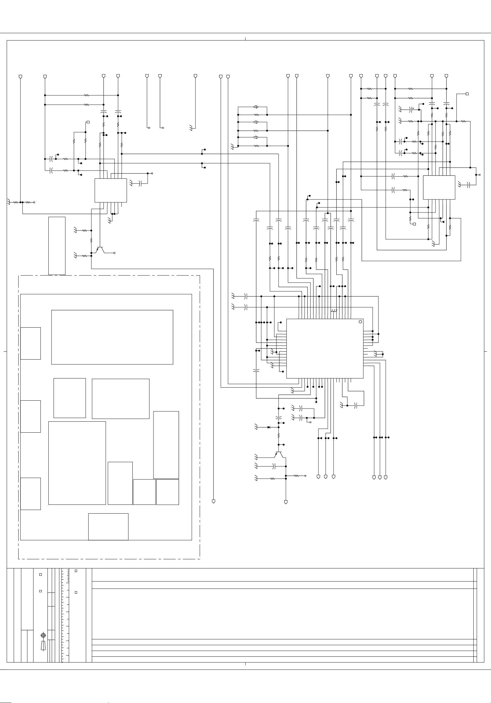
AV_SWITCH BLOCK
470N
10%
C36
TP7
TP65
TP68
TP4
C37
10%
1U
IC2, IC3, IC4, IC5
AUDIO_BLOCK
CN3 CN1
PLEASE LAYOUT THE FUNCTIONALITY OF THE DESIGN AS SHOWN BELOW:
AV_SWITCH_BLOCK
IC7 & IC19
CN2
IC16,18,17 on underside.
on underside
POWER_SUPPLY_BLOCK
IC10
Locate IC1 in
middle of pwb
& TR3
VIDEO_BUFFER
BLOCK
AV_SWITCH_BLOCK
IC1 & Passives
ICs 8,9
I2C_BLOCK
MICROPROCESSOR (IC11 & IC6)
IR_INTERFACE
IC12,13 &14
VOLVO_AUDIO_SEL_DRIVE
TP82
TP84
TP81 TP78
C3
10%
470N
BAS16
10%
1U
D1
BC817-25
10K5%R47
TP8
S2-3
20
20
S-3
21
21
V4
22
22
LV4
23
23
Y4
24
24
RV4
25
25
C4
26
26
S2-4
27
27
S-4
28
28
LV5
29
29
V5
30
30
RV5
31
31
ADR
32
32
SCL33SDA
TP9
C4
10%
R61
75
5%
TP47TP46TP80
TR3
C39
10%
1U
47K5%R45
9VSENSE
13
17
15
19181716131211
18
151410
LV316Y3
S-214V3
RV319C3
DC-OUT
COUT338LOUT339YOUT3
ROUT341VOUT3
AGND
35
36
37
40
40439383736353433
34
TP5
TP3
TP1
C675%10P
TP79
+9VA
100N
C14
LOUT2
+9VA
TO AUDIO_VIDEO BLOCK C24
10
8
987
RV211C212S2-2
S-17V2
LV29Y2
CXA2069Q
IC1
LOUT243VOUT244ROUT2
VCC
42
TP2
TP72
TP75
VOUT2
TO AUDIO_VIDEO BLOCK C25
TO VIDEO_BUFFER BLOCK C45 (REF SHEET7)
45
4544434241
TP76
ROUT2
S2-1
1
2
3
4
5
6
6
3
2
1
V1
LV1
Y1
RV1
C1
RTV
64
64
TV
63
63
LTV
62
62
RV6
61
61
V6
60
60
LV6
59
59
COUT1
58
58
VGND
57
57
YOUT1
56
56
TRAP1
55
55
ROUT1
54
54
VOUT1
53
53
LOUT1
COUT247TRAP2
MUTE
BIAS
YIN149CIN1
48
50
46
494647
50548
52
52
51
51
100N
10%
C26
TP71
TP74
TP73
VOUT1
LOUT1
ROUT1
TO AUDIO_VIDEO BLOCK C16
TO VIDEO_BUFFER BLOCK C44
TO AUDIO_VIDEO BLOCK C15
NAME
NO.
MS-XXXX-3458-XX
PWB
SKETCH - WIRING DIAGRAM
(DRAWING_NAME)
PLANT CODE:
DATE
POWERVIEW
MATERIAL
ANGULAR DIM. +/-
MACHINED DIM. +/-
INCHES
MILLIMETERS
STAMPED DIM. +/-
3RD ANGLE PROJECTION
APP
UNLESS OTHERWISE SPECIFIED:
REF PROJECT/SCH/SCH_NAME
DIMENSIONS ARE IN
DO NOT SCALE
DRAWN BY
YYMMDD
DATE
ABOVE SCALE FOR REFERENCE ONLY
CHECKED APPROVEDSCALE
NONE
METRIC20 30 40 50 100 110 120 13060 70 80 90
CG COLUMN = GRAPHIC DATA LEVEL ORIGINAL WHEN RED
ENGLISH
*
Visteon
COMPUTER
MANUAL
256
PRODUCT ENGINEERING
"E"
3
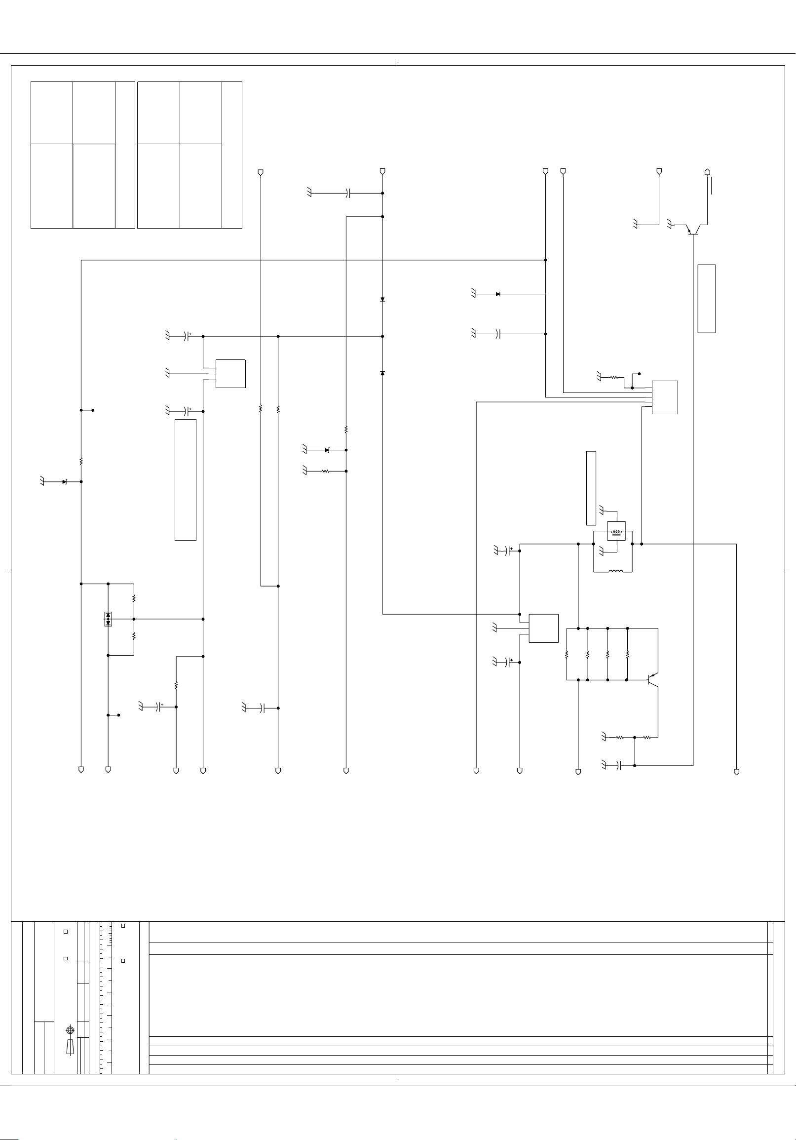
SIZE
41
140 150 160
CN4
TO HELP SAFEGUARD HEALTH, SAFETY AND THE ENVIRONMENT
PART MUST COMPLY WITH SPECIFICATION WSS-M99P9999-A1
TO IC11 PIN 17
(REF SHEET5)
(REF SHEET5)
(REF SHEET5)
(REF SHEET7)
(REF SHEET5)
30.10.01 R105 is now 1.2K.
21.06.01 TP87, TP114 deleted - no space.
R102 changed to 56.2K 1%.
09.04.01 All Grounds are now GND.
19.06.01 C89 is now connected to gnd plane earth.
08.06.01 Test points added to circuitTP90
27.03.01 TP78 ADDED.
19.03.01 R79 is now 10K 5%.
12.03.01 IC7 & IC19 now correct components.
12.03.01 AUDIO1..AUDIO3_GND added.
12.03.01 Placement Notes mod’d after review.
16.03.01 C89,90,91 changed to 16V to
25.05.01 IC7 & IC19 reconfigured to
TP95,TP96 deleted - no space.
C61 is now 33uF.
C61,C90,C91 added.
minimise size.
Audio Inputs.
around IC7 & IC19.
be differential amp buffer for
01.03.01 First Revision for Checking
NO.
MS-XXXX-3458-XX
SHEET OF
CGDATE LET REVISIONS MAN CK APP
2
7
##
Page 21
TO POWER_SUPPLY BLOCK D8
(REF SHEET4)
TO CN3 PIN 12
GND
2.2K
5%
TO CN4 PIN 14
IR2
2.2K
5%
R49
TO CN4 PIN 4
IR1
10P5%C94
2.2K
5%
R48
TO CN3 PIN 3
NOTE: PLACE C94 NEAR TO CN3 PIN3.
IR0
R59
8
8
7A16A25
GND
E1
IN74IN63IN5
74HC148
IN3
IN011IN112IN2
A0
9
13
10
9
GS14E0
+5V_VIA_D8
47K5%R38
TP49 TP50 TP51 TP52
47K5%R39
47K5%R40
47K5%R41
1234567
2
1
IN4
IC12
VCC
16151413121110
16
15
+5V_VIA_D8
(VIA)
TP54
(VIA)
TP53
+5V_VIA_D8
69
5
7
432
DATA1
CLOCK1
SET1
GND
Q1
Q1
74HC74A
CLOCK2
RESET2
DATA2
SET2
Q2
Q2
8
TP57
1
RESET1
VCC
1413121110
C51
10%
100N
10P5%C68
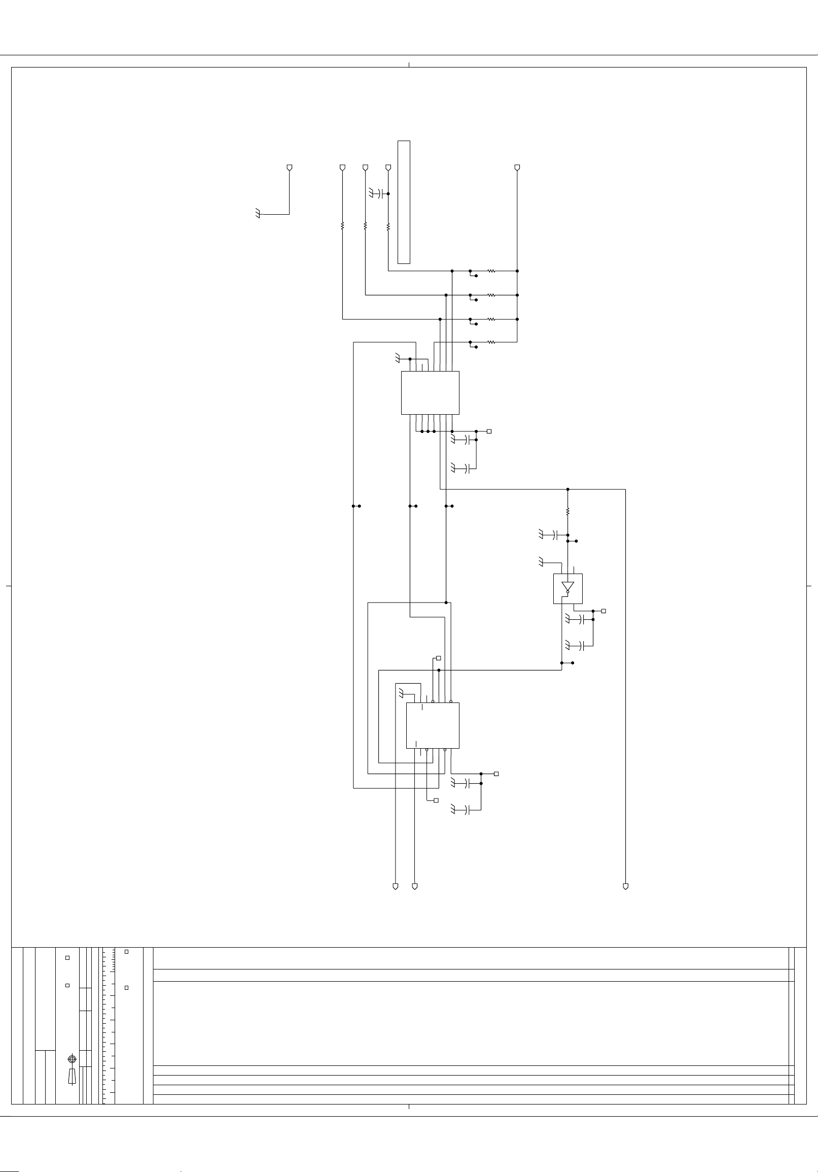
IR_INTERFACE BLOCK
100
5%
R42
470P5%C50
TP55
321
NCAGND
BU4S584
IC14
+5V_VIA_D8
100N
10%
C56
C695%10P
IC13
+5V_VIA_D8
VCC
Y
4
5
TP56
(VIA)
NAME
NO.
MS-XXXX-3458-XX
PWB
SKETCH - WIRING DIAGRAM
(DRAWING_NAME)
PLANT CODE:
DATE
POWERVIEW
MATERIAL
ANGULAR DIM. +/-
MACHINED DIM. +/-
INCHES
MILLIMETERS
STAMPED DIM. +/-
3RD ANGLE PROJECTION
APP
UNLESS OTHERWISE SPECIFIED:
REF PROJECT/SCH/SCH_NAME
DIMENSIONS ARE IN
DO NOT SCALE
DRAWN BY
YYMMDD
DATE
ABOVE SCALE FOR REFERENCE ONLY
CHECKED APPROVEDSCALE
NONE
METRIC20 30 40 50 100 110 120 13060 70 80 90
CG COLUMN = GRAPHIC DATA LEVEL ORIGINAL WHEN RED
ENGLISH
*
Visteon
COMPUTER
MANUAL
256
PRODUCT ENGINEERING
"E"
3
SIZE
41
140 150 160
TO HELP SAFEGUARD HEALTH, SAFETY AND THE ENVIRONMENT
PART MUST COMPLY WITH SPECIFICATION WSS-M99P9999-A1
IR_STATUS0
TO IC11 PIN 1
(REF SHEET1)
IR_STATUS1
TO IC11 PIN 20
(REF SHEET1)
+5V_VIA_D8
100N
10%
C55
C705%10P
INT1
(REF SHEET1)
TO IC11 PIN 8
12.03.01 ECAD review. No change in this FUB.
01.03.01 First Revision for Checking
16.03.01 C94 added.
NO.
MS-XXXX-3458-XX
SHEET OF
CGDATE LET REVISIONS MAN CK APP
3
7
##
Page 22
CODE.
WITH SECURITY
MCB SOFTWARE
CASE B:
MCB SOFTWARE
WITHOUT SECURITY
CODE.
D8,R60,Z1, LK3 NOT
FITTED.
LK1,LK2 & LK4 FITTED.CASE A:
LINK TABLE
FOR VOLVO
MCB SOFTWARE
WITH SECURITY
CODE.
CASE B:
CASE A:
MCB SOFTWARE
WITHOUT SECURITY
CODE.
LK1,LK2 & LK3 FITTED.
D8,R60,Z1, LK4 NOT
FITTED.
FOR NON_VOLVO
LINK TABLE
TO AV_SWITCH FUB
TO CN1 PIN 1
CN2 PIN 1
TO TR6,R53 (SHEET 1)
TO CN1 PIN 6
TO CN3 PIN 12
TO CN2 PIN 12
TO IC11 PIN 4
500MW5%5.1V
Z1
27K
5%
TP48
R60
(5.1V NOMINAL.)
C63
20%
100U
2A max
1
I
2
GND
3
Q
100U
20%
C64
NOTE:..Ensure that the +5V line
is STARPOINTED from the
C64 BULK CAPACITOR.
VOLVO_AUDIO_SEL_DRIVE
2A max
BA178M05FP
IC17
LK4
%
0
LK3
%
0
NOTE: LK4 ONLY FITTED FOR VOLVO (LK3 MUST BE REMOVED)
1A max (to allow for S/C conditions in AUX Panel)
500MW5%5.1V
Z2
R375%3.3K
ACC
C60
10%
100N
2A max 2A max
400V
GF-1
1A
ACC
5.6K
5%
R34
D3
400V
GF-1
1A
D4
400V
D2
3A
S3G
C59
10%
100N
2A max
VBAT
6A max
POWERSW
1505%R46
FIT EITHER L1 OR L1a
TP61
1
GND
2
IN
3
VBB
4
ST
5
OUT
6A max
MMBTA06
IC16
TR5
approx. 7V
RESET
switch down to
Sense Circuit will
GND
225MW
500MA
BTS426L1
POWER_SUPPLY BLOCK
200MA
70V
0.5A max
+5V_BATTF
(REF SHEET1)
TO R43
BAW56
D8
0.5A max
+5V_VIA_D8
(REF SHEET3)
TO IR_INTERFACE FUB
TP58
(VIA)
2A max
L1A
2
3
1
4
C49
20%
3.3M
25V
2A max 2A max
LK2
0
1
I
2
33U
20%
C62
GND
3
Q
+9VA
TO AV_SWITCH BLOCK
(REF. SHEET 2)
LK1
0
R44
5%
2.2
100U
20%
C65
2A max
1A max
C93
10%
100N
ACC_VIA_DIODE
VCC
(REF SHEET 7)
TO VIDEO_BUFFER BLOCK
NOTE:
FIT CAP C93 NEAR CN3 PIN8
+5V
TO CN3 PIN 6
(REF SHEET1)
+5V_ACC
(REF SHEET1)
TO IC11 PIN 13
ISENSE
TO IC1 PIN 14 (SHEET 2)
(REF. SHEET 2)
TO AV_SWITCH BLOCK
4A max
BA178M09FP
IC18
R73
5%
1
5%
4A max
(12S)VFILTER
TO CN4 PINs 6 & 16, 10 & 20
500U
L1
6A max
500MA
MMBTA56
225MW
R72
1
1
5%
R74
R69
1
5%
TR4
3.3K5%R68
27K5%R67
C92 is to prevent TR5 from turning on
in response to start up surge currents in
LCD panel caps.
Overcurrent Limit= 2.8A approx.
Pd at near Overcurrent limit but not
shutdown = 2.8A*2.8A**0.25=1.96W.
=> each Resistor sustains 1.96/4 = 0.5W
C92
10%
1U
Normal Pd = 1.8A*1.8A*0.25 =0.81W.
Combined R69,R72,R73&R74 = 0.25 Ohms
DESIGN NOTE:
CN2 PINS 3 & 4 (DVD)
SBATT
(+12R)
TO CN1 PINs 3 & 4 (VCR)
NAME
NO.
MS-XXXX-3458-XX
PWB
SKETCH - WIRING DIAGRAM
(DRAWING_NAME)
PLANT CODE:
DATE
POWERVIEW
MATERIAL
ANGULAR DIM. +/-
MACHINED DIM. +/-
INCHES
MILLIMETERS
STAMPED DIM. +/-
3RD ANGLE PROJECTION
APP
UNLESS OTHERWISE SPECIFIED:
REF PROJECT/SCH/SCH_NAME
DIMENSIONS ARE IN
DO NOT SCALE
DRAWN BY
YYMMDD
DATE
ABOVE SCALE FOR REFERENCE ONLY
CHECKED APPROVEDSCALE
NONE
METRIC20 30 40 50 100 110 120 13060 70 80 90
CG COLUMN = GRAPHIC DATA LEVEL ORIGINAL WHEN RED
ENGLISH
*
Visteon
COMPUTER
MANUAL
256
PRODUCT ENGINEERING
"E"
3
SIZE
41
140 150 160
TO HELP SAFEGUARD HEALTH, SAFETY AND THE ENVIRONMENT
PART MUST COMPLY WITH SPECIFICATION WSS-M99P9999-A1
08.06.01 VOLVO_AUDIO_SEL_DRIVE signal
02.04.01 R71 removed.
27.03.01 C63,64,65 are now 100uF 35V.
14.06.01 Text added for clarification.
09.04.01 All Grounds are now GND.
added.
Text changes for clarification.
BATTF label deleted.
15.03.01 All Tie-points removed as they are
19.03.01 PIN 2&4 of L1a now conn. to GNDS.
16.03.01 TP58 added.
23.03.01 BATTF FUB conn. added.
14.03.01 IC17&18 edited to show correct
Notes added for clarification.
Visula.
pkg_type.
C93 added.
Track Currents added.
treated as additional components in
13.03.01 C92 added to create ’SOFT START’
01.03.01 First Revision for Checking
12.03.01 ECAD review C61 2200uF deleted
NO.
MS-XXXX-3458-XX
for overcurrent sense.
owing to space limitation.
SHEET OF
CGDATE LET REVISIONS MAN CK APP
4
7
##
Page 23
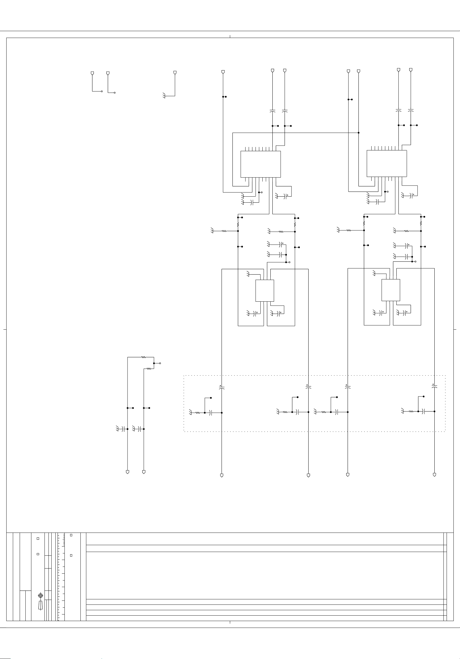
+9VA
+9VA
To drain of TR1
SDA1
To IC11 pin 10
SCL
TP10
(VIA)
To IC1 pin 52
LOUT1
10%
1U
C16
TP12
To IC1 pin 54
ROUT1
1U
10%
C15
TP11
To drain of TR2
+5V
+5V
GND
SDA2
TP19
(VIA)
To IC1 pin 43
LOUT2
10%
1U
C25
TP21
To IC1 pin 45
ROUT2
1U
10%
C24
TP20
10 11
8
9
7
AM
MPX
LEVEL SMUTE
PHGND
PHONE
TDA7460
SCL
SDA
GND
VDD
121314151617181920
100N
10%
C75
TP23
2.2K
5%
R27
R21
100
5%
TP25
TDA2822D
6
-IN2GND
CDL
OUT_RR
54
+9VA
321
OUT2
+IN2
CDGND
OUT_LR
VCC
+IN1
CDR
OUT_RF
16V
OUT1
-IN1
876
CASS_L
OUT_LF
10U
20%
100N
10%
12345
CASS_R
CREF
C96
C27
IC4
16V
1005%R20
IC5
10U
20%
C30
TP22
2.2K
5%
R26
TP24
+9VA
1005%R17
2.2K
5%
TDA7460
R25
TP16
TP14
LEVEL SMUTE
1110
9
8
AM
MPX
PHONE
SCL
SDA
GND
100N
10%
C74
7
6
54321
CASS_R
CASS_L
CDR
CDGND
CDL
PHGND
OUT_RR
OUT_LR
OUT_RF
OUT_LF
CREF
VDD
201918171615141312
+9VA
16V
10U
20%
C95
C17
10%
100N
123
45
OUT2
VCC
OUT1
TDA2822D
IC3
-IN1
+IN1
+IN2
-IN2GND
678
1005%R16
IC2
C28
20%
10U
16V
TP13
2.2K
5%
R24
AUDIO_OUTPUT BLOCK
TP15
+9VA
100N
10%
TP31
C76
SEL2
TO CN4 PIN 15
100N
10%
R565%220
TP30
C77
SEL1
TO CN4 PIN 5
100U
20%
100U
20%
100U
20%
C34
+5V
R555%220
100U
20%
C31
TP27
4.75%R23
100N
10%
C33
R2
TO CN3 PIN 4
100U
20%
C35
100U
20%
C29
TP26
4.75%R22
100N
10%
C32
NOTE: Keep these components in the dotted areas
in close proximity with IC3 and IC4.
L2
TO CN3 PIN 5
4.75%R19
TP18
10%
100N
C23
100U
20%
C21
R1
TO CN3 PIN 1
C19
C18
100U
20%
C20
TP17
4.75%R18
100N
10%
C22
L1
TO CN3 PIN 2
NAME
NO.
MS-XXXX-3458-XX
PWB
SKETCH - WIRING DIAGRAM
(DRAWING_NAME)
PLANT CODE:
DATE
POWERVIEW
MATERIAL
ANGULAR DIM. +/-
MACHINED DIM. +/-
INCHES
MILLIMETERS
STAMPED DIM. +/-
3RD ANGLE PROJECTION
APP
UNLESS OTHERWISE SPECIFIED:
REF PROJECT/SCH/SCH_NAME
DIMENSIONS ARE IN
DO NOT SCALE
DRAWN BY
YYMMDD
DATE
ABOVE SCALE FOR REFERENCE ONLY
CHECKED APPROVEDSCALE
NONE
METRIC20 30 40 50 100 110 120 13060 70 80 90
CG COLUMN = GRAPHIC DATA LEVEL ORIGINAL WHEN RED
ENGLISH
*
Visteon
COMPUTER
MANUAL
256
PRODUCT ENGINEERING
"E"
3
SIZE
41
140 150 160
TO HELP SAFEGUARD HEALTH, SAFETY AND THE ENVIRONMENT
PART MUST COMPLY WITH SPECIFICATION WSS-M99P9999-A1
09.04.01 All Grounds are now GND.
25.05.01 10uF caps added to supply pin of
14.03.01 C28&C30 now 16V parts.
01.03.01 First Revision for Checking.
12.03.01 IC8,IC9 Ckts transferred to
NO.
MS-XXXX-3458-XX
Extra explanatory text added.
FUB after ECAD review to improve
clarity in LAYOUT notes.
both IC3 & IC4.
IC10 Ckts transferred to VIDEO_BUFFER
I2C FUB after ECAD review.
SHEET OF
CGDATE LET REVISIONS MAN CK APP
5
7
##
Page 24
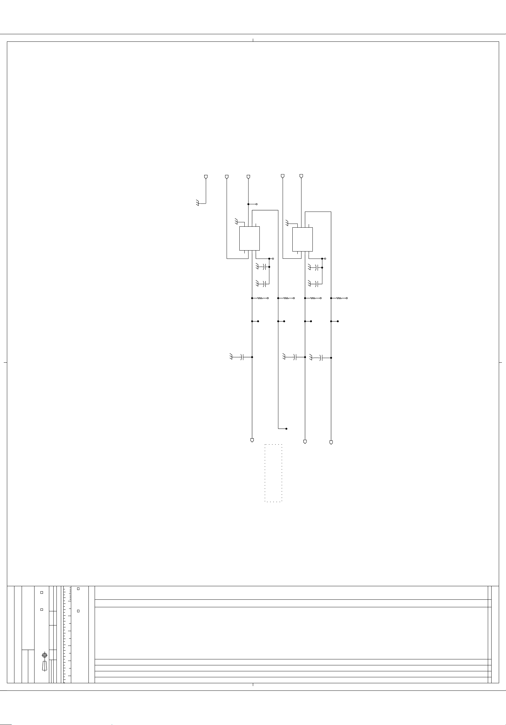
SDA1
GND
SCL
+5V
SDA2
+5V
1
432
P82B715TD
NC
587
NC
LXSXGND
IC9
VCC
SY
LY
6
+5V
100N
10%
C43
432
P82B715TD
SY
NC
587
1
NC
LXSXGND
IC8
VCC
LY
6
+5V
100N
10%
C42
10P5%C80
C725%10P
+5V
1505%R31
TP32
XSCL
TO CN4 PINs 2 & 12
+5V
1505%R30
TP33
10P5%C79
XSDA3
TP6
Keep C76,C77,C78,C79,C80,
Note:
near connector side.
1505%R29
TP29
(VIA)
XSDA2
TO CN4 PIN 11
10P5%C71
C785%10P
+5V
+5V
1505%R28
I2C BUFFER BLOCK
TP28
(VIA)
XSDA1
TO CN4 PIN 1
NAME
NO.
MS-XXXX-3458-XX
PWB
SKETCH - WIRING DIAGRAM
(DRAWING_NAME)
PLANT CODE:
DATE
POWERVIEW
MATERIAL
ANGULAR DIM. +/-
MACHINED DIM. +/-
INCHES
MILLIMETERS
STAMPED DIM. +/-
3RD ANGLE PROJECTION
APP
UNLESS OTHERWISE SPECIFIED:
REF PROJECT/SCH/SCH_NAME
DIMENSIONS ARE IN
DO NOT SCALE
DRAWN BY
YYMMDD
DATE
ABOVE SCALE FOR REFERENCE ONLY
CHECKED APPROVEDSCALE
NONE
METRIC20 30 40 50 100 110 120 13060 70 80 90
CG COLUMN = GRAPHIC DATA LEVEL ORIGINAL WHEN RED
ENGLISH
*
Visteon
COMPUTER
MANUAL
256
PRODUCT ENGINEERING
"E"
3
SIZE
41
140 150 160
TO HELP SAFEGUARD HEALTH, SAFETY AND THE ENVIRONMENT
PART MUST COMPLY WITH SPECIFICATION WSS-M99P9999-A1
09.04.01 All Grounds are now GND.
29.03.01 Text added for Notes.
12.03.01 FUB created after ECAD review
NO.
MS-XXXX-3458-XX
to allow clarity in ECAD layout.
SHEET OF
CGDATE LET REVISIONS MAN CK APP
6
7
##
Page 25
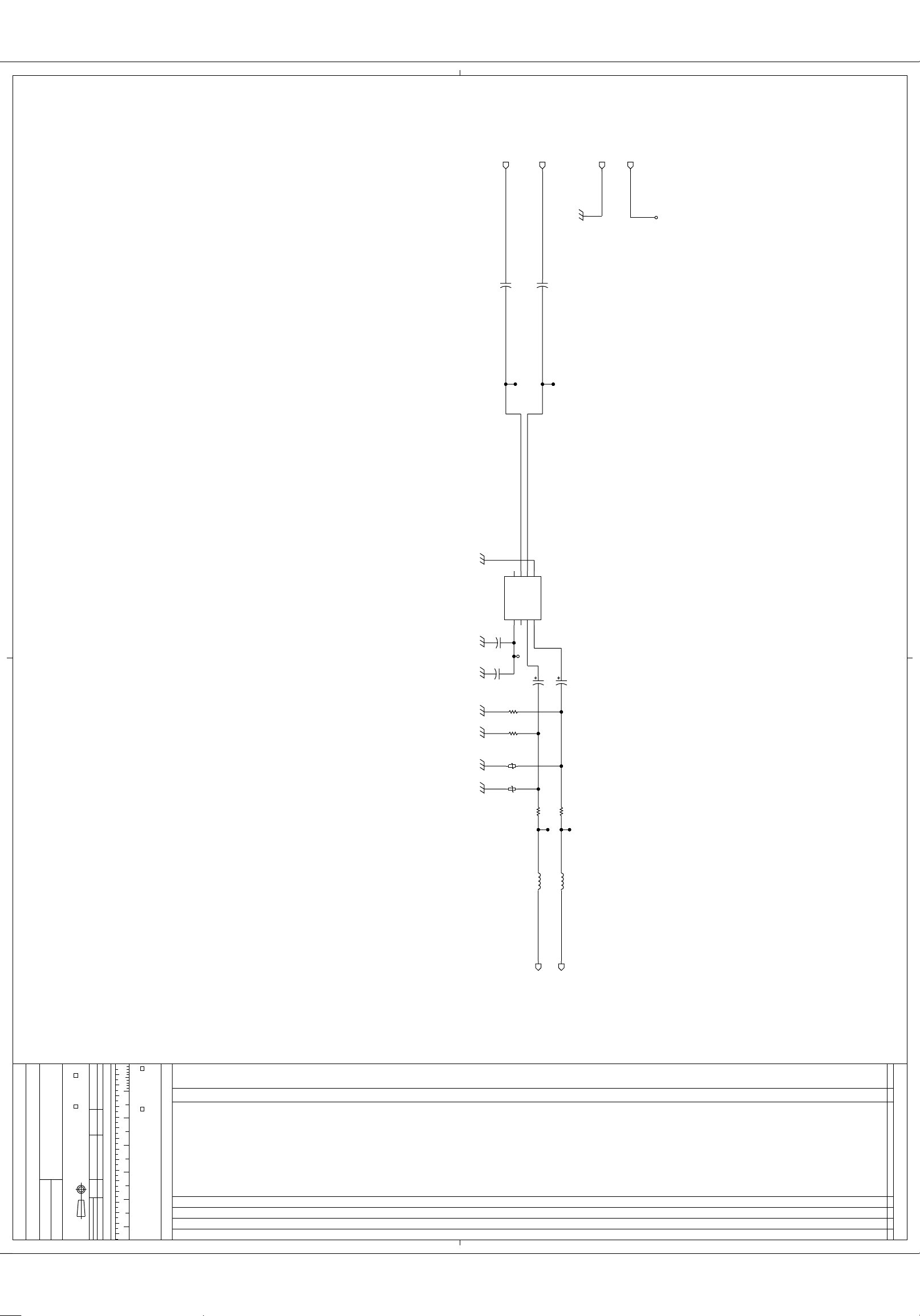
TO IC1 PIN 44
TO IC1 PIN 53
VOUT2
10%
VOUT1
GND
VCC
VCC
10%
1U
1U
TP37
C44
TP36
C45
10%
100N
10P5%C73
IN3
BA7622F
VCC
C46
IN2
OUT3
R325%10K
R335%10K
RV19RV18
2
IN1
OUT2
678
VCC
5%
1345
GND
IC10
OUT1
C48
20%
470U
20%
470U
75
R36
5%
75
TP35
L9
C47
R35
TP34
L8
NAME
NO.
MS-XXXX-3458-XX
PWB
SKETCH - WIRING DIAGRAM
(DRAWING_NAME)
PLANT CODE:
DATE
POWERVIEW
MATERIAL
ANGULAR DIM. +/-
MACHINED DIM. +/-
INCHES
MILLIMETERS
STAMPED DIM. +/-
3RD ANGLE PROJECTION
APP
UNLESS OTHERWISE SPECIFIED:
REF PROJECT/SCH/SCH_NAME
DIMENSIONS ARE IN
DO NOT SCALE
DRAWN BY
YYMMDD
DATE
ABOVE SCALE FOR REFERENCE ONLY
CHECKED APPROVEDSCALE
NONE
METRIC20 30 40 50 100 110 120 13060 70 80 90
CG COLUMN = GRAPHIC DATA LEVEL ORIGINAL WHEN RED
ENGLISH
*
Visteon
COMPUTER
MANUAL
256
PRODUCT ENGINEERING
"E"
3
SIZE
41
140 150 160
TO HELP SAFEGUARD HEALTH, SAFETY AND THE ENVIRONMENT
PART MUST COMPLY WITH SPECIFICATION WSS-M99P9999-A1
VIDEO_OUT2
TO CN4 PIN 18
VIDEO_OUT1
TO CN4 PIN 8
09.04.01 All Grounds are now GND.
30.03.01 MORE TEXT ADDED FOR NOTES,
12.03.01 FUB created to clarify lay-out
NO.
MS-XXXX-3458-XX
partitioningafter ECAD review.
SHEET OF
CGDATE LET REVISIONS MAN CK APP
77
##
 Loading...