

Realtek Semiconductor RTL8187SE User Manual

RTL8187SE
SINGLE-CHIP WIRELESS LAN NETWORK
INTERFACE CONTROLLER w/PCI EXPRESS
INTERFACE
DATASHEET
16 January 2008
Track ID: JATR-1076-21
Rev. 1.0
Realtek Semiconductor Corp.
No. 2, Innovation Road II, Hsinchu Science Park, Hsinchu 300, Taiwan
Tel.: +886-3-578-0211. Fax: +886-3-577-6047
www.realtek.com.tw

RTL8187SE
Datasheet
COPYRIGHT
©2008 Realtek Semiconductor Corp. All rights reserved. No part of this document may be reproduced,
transmitted, transcribed, stored in a retrieval system, or translated into any langµAge in any form or by any
means without the written permission of Realtek Semiconductor Corp.
DISCLAIMER
Realtek provides this document “as is”, without warranty of any kind, neither expressed nor implied,
including, but not limited to, the particular purpose. Realtek may make improvements and/or changes in
this document or in the product described in this document at any time. This document could include
technical inaccuracies or typographical errors.
TRADEMARKS
Realtek is a trademark of Realtek Semiconductor Corporation. Other names mentioned in this document are
trademarks/registered trademarks of their respective owners.
CONFIDENTIALITY
This document is confidential and should not be provided to a third-party without the permission of Realtek
Semiconductor Corporation.
USING THIS DOCUMENT
This document is intended for the software engineer’s reference and provides detailed programming
information.
Though every effort has been made to ensure that this document is current and accurate, more information
may have become available subsequent to the production of this guide. In that event, please contact your
Realtek representative for additional information that may help in the development process.
REVISION HISTORY
Revision Release Date Summary
1.0 2008/01/16 First release.
Single-Chip Wireless LAN Network Interface Controller
w/PCI Express Interface
ii
Track ID: JATR-1076-21 Rev. 1.0

RTL8187SE
Datasheet
Table of Contents
1. GENERAL DESCRIPTION ...............................................................................................................................................1
2. FEATURES ..........................................................................................................................................................................3
3. SYSTEM APPLICATIONS ................................................................................................................................................4
4. BLOCK DIAGRAMS ..........................................................................................................................................................5
5. PIN ASSIGNMENTS...........................................................................................................................................................7
5.1. PACKAGE IDENTIFICATION ..............................................................................................................................................7
6. PIN DESCRIPTIONS ..........................................................................................................................................................8
6.1. POWER MANAGEMENT/ISOLATION INTERFACE ...............................................................................................................8
6.2. PCI EXPRESS INTERFACE ............................................................................................................................... .................8
6.3. EEPROM INTERFACE .....................................................................................................................................................9
6.4. POWER PINS ....................................................................................................................................................................9
6.5. LED INTERFACE............................................................................................................................................................10
6.6. BASEBAND AND RF PINS............................................................................................................................... ................10
6.7. BLUETOOTH CO-EXISTENCE PINS ............................................................................................................................... ..11
6.8. CLOCK AND OTHER PINS...............................................................................................................................................11
7. EEPROM (93C46 OR 93C56) CONTENTS ....................................................................................................................11
8. PCI EXPRESSTM............................................................................................................................... .................................12
8.1. PCI EXPRESS BUS INTERFACE....................................................................................................................................12
8.1.1. PCI Express Transmitter ......................................................................................................................................12
8.1.2. PCI Express Receiver........................................................................................................... ................................12
8.2. PCI CONFIGURATION SPACE TABLE..............................................................................................................................1 3
8.3. PCI CONFIGURATION SPACE FUNCTIONS ......................................................................................................................16
8.4. PCI CONFIGURATION SPACE STATUS............................................................................................................................17
8.4.1. Status ....................................................................................................................................................................17
8.4.2. RIDR (Revision ID Register) ................................................................................................................................18
8.4.3. PIFR (Programming Interface Register)..............................................................................................................18
8.4.4. SCR (Sub-Class Register).....................................................................................................................................18
8.4.5. BCR (Base-Class Register)...................................................................................................................................18
8.4.6. CLS (Cache Line Size)..........................................................................................................................................18
8.4.7. LTR (Latency Timer Register) ..............................................................................................................................18
8.4.8. HTR (Header Type Register)................................................................................................................................18
8.4.9. BIST (Built-In Self-Test) .......................................................................................................................................18
8.4.10. IOAR (Input Output Address Register).................................................................................................................19
8.4.11. MEMAR (Memory Address Register) ...................................................................................................................19
8.4.12. CISPtr (CardBus Card Information Structure Pointer) .......................................................................................19
8.4.13. SVID (Subsystem Vendor ID) ...............................................................................................................................20
8.4.14. SMID (Subsystem ID)............................................................................................................ ...............................20
8.4.15. ILR (Interrupt Line Register)................................................................................................................................20
8.4.16. IPR (Interrupt Pin Register).................................................................................................................................20
8.4.17. MNGNT (Minimum Grant Timer: Read only)......................................................................................................20
8.4.18. MXLAT (Maximum Latency Timer: Read only) ...................................................................................................20
8.5. DEFAULT VALUE AFTER POWER-ON (RSTB ASSERTED)..............................................................................................20
Single-Chip Wireless LAN Network Interface Controller
w/PCI Express Interface
iii
Track ID: JATR-1076-21 Rev. 1.0

RTL8187SE
Datasheet
8.6. PCI POWER MANAGEMENT FUNCTIONS ........................................................................................................................22
8.7. MESSAGE SIGNALED INTERRUPT (MSI) ........................................................................................................................25
8.7.1. MSI Capability Structure in PCI Configuration Space ........................................................................................25
8.7.2. Message Control...................................................................................................................................................26
8.7.3. Message Address ..................................................................................................................................................26
8.7.4. Message Upper Address.......................................................................................................... .............................27
8.7.5. Message Data .......................................................................................................................................................27
9. FUNCTIONAL DESCRIPTION ......................................................................................................................................28
9.1. TRANSMIT & RECEIVE OPERATIONS .............................................................................................................................28
9.1.1. Transmit ...............................................................................................................................................................28
9.1.2. Receive .................................................................................................................................................................35
9.2. LOOPBACK OPERATION.................................................................................................................................................39
9.3. QOS FUNCTIONS ...........................................................................................................................................................39
9.4. LED FUNCTIONS............................................................................................................................... ............................39
10. APPLICATION DIAGRAM .........................................................................................................................................40
11. ELECTRICAL CHARACTERISTICS........................................................................................................................41
11.1. TEMPERATURE LIMIT RATINGS .................................................................................................................................41
11.2. DC CHARACTERISTICS ..............................................................................................................................................41
11.3. AC CHARACTERISTICS ..............................................................................................................................................42
11.3.1. Serial EEPROM Interface Timing (93C46(64*16)/93C56(128*16))...................................................................42
11.4. PCI EXPRESS BUS PARAMETERS ...............................................................................................................................43
11.4.1. Differential Transmitter Parameters ....................................................................................................................43
11.4.2. Differential Receiver Parameters.........................................................................................................................44
11.4.3. REFCLK Parameters ...........................................................................................................................................44
11.4.4. Auxiliary Signal Timing Parameters ....................................................................................................................48
12. MECHANICAL DIMENSIONS ...................................................................................................................................49
13. ORDERING INFORMATION .....................................................................................................................................50
Single-Chip Wireless LAN Network Interface Controller
w/PCI Express Interface
iv
Track ID: JATR-1076-21 Rev. 1.0

RTL8187SE
Datasheet
List of Tables
TABLE 1. POWER MANAGEMENT/ISOLATION INTERFACE ..............................................................................................................8
TABLE 2. PCI EXPRESS INTERFACE ...............................................................................................................................................8
TABLE 3. EEPROM INTERFACE ....................................................................................................................................................9
TABLE 4. POWER PINS ...................................................................................................................................................................9
TABLE 5. LED INTERFACE...........................................................................................................................................................10
TABLE 6. BASEBAND AND RF PINS..............................................................................................................................................10
TABLE 7. BLUETOOTH CO-EXISTENCE PINS ................................................................................................................................11
TABLE 8. CLOCK AND OTHER PINS............................................................................................................................... ...............11
TABLE 9. PCI CONFIGURATION SPACE TABLE.............................................................................................................................13
TABLE 10. COMMAND REGISTER IN PCI CONFIGURATION SPACE.................................................................................................16
TABLE 11. PCI CONFIGURATION SPACE STATUS...........................................................................................................................17
TABLE 12. INPUT OUTPUT ADDRESS REGISTER.............................................................................................................................19
TABLE 13. MEMORY ADDRESS REGISTER .....................................................................................................................................19
TABLE 14. PCI CONFIGURATION SPACE TABLE ............................................................................................................................20
TABLE 15. MESSAGE CONTROL.....................................................................................................................................................26
TABLE 16. MESSAGE ADDRESS .....................................................................................................................................................26
TABLE 17. MESSAGE UPPER ADDRESS..........................................................................................................................................27
TABLE 18. MESSAGE DATA............................................................................................................................... ............................27
TABLE 19. TX DESCRIPTOR FORMAT (BEFORE TRANSMITTING, OWN=1, TX COMMAND MODE 1)................................................28
TABLE 20. TX STATUS DESCRIPTOR............................................................................................................................... ...............30
TABLE 21. TX STATUS DESCRIPTOR (AFTER TRANSMITTING, OWN=0, TX STATUS MODE)...........................................................33
TABLE 22. TX STATUS DESCRIPTOR (AFTER TRANSMITTING, OWN=0, TX STATUS MODE)...........................................................34
TABLE 23. RX COMMAND DESCRIPTOR (OWN=1) .......................................................................................................................35
TABLE 24. RX COMMAND DESCRIPTOR (OWN=1) .......................................................................................................................35
TABLE 25. RX STATUS DESCRIPTOR (OWN=0) ........................................................................................................................ ....36
TABLE 26. RX STATUS DESCRIPTOR..............................................................................................................................................37
TABLE 27. TEMPERATURE LIMIT RATINGS............................................................................................................................... .....41
TABLE 28. DC CHARACTERISTICS.................................................................................................................................................41
TABLE 29. EEPROM ACCESS TIMING PARAMETERS ....................................................................................................................42
TABLE 30. DIFFERENTIAL TRANSMITTER PARAMETERS................................................................................................................43
TABLE 31. DIFFERENTIAL RECEIVER PARAMETERS.......................................................................................................................44
TABLE 32. REFCLK PARAMETERS ...............................................................................................................................................44
TABLE 33. AUXILIARY SIGNAL TIMING PARAMETERS...................................................................................................................48
TABLE 34. ORDERING INFORMATION ............................................................................................................................................50
Single-Chip Wireless LAN Network Interface Controller
w/PCI Express Interface
v
Track ID: JATR-1076-21 Rev. 1.0

RTL8187SE
Datasheet
List of Figures
FIGURE 1. BLOCK DIAGRAM............................................................................................................................... ...........................5
FIGURE 2. RF BLOCK DIAGRAM ....................................................................................................................................................6
FIGURE 3. PIN ASSIGNMENTS............................................................................................................................... ..........................7
FIGURE 4. MESSAGE CAPABILITY STRUCTURE ............................................................................................................................25
FIGURE 5. APPLICATION DIAGRAM..............................................................................................................................................40
FIGURE 6. SERIAL EEPROM INTERFACE TIMING........................................................................................................................42
FIGURE 7. SINGLE-ENDED MEASUREMENT POINTS FOR ABSOLUTE CROSS POINT AND SWING ...................................................46
FIGURE 8. SINGLE-ENDED MEASUREMENT POINTS FOR DELTA CROSS POINT.............................................................................46
FIGURE 9. SINGLE-ENDED MEASUREMENT POINTS FOR RISE AND FALL TIME MATCHING..........................................................46
FIGURE 10. DIFFERENTIAL MEASUREMENT POINTS FOR DUTY CYCLE AND PERIOD .....................................................................47
FIGURE 11. DIFFERENTIAL MEASUREMENT POINTS FOR RISE AND FALL TIME .............................................................................47
FIGURE 12. DIFFERENTIAL MEASUREMENT POINTS FOR RINGBACK..............................................................................................47
FIGURE 13. REFERENCE CLOCK SYSTEM MEASUREMENT POINT AND LOADING ...........................................................................48
FIGURE 14. AUXILIARY SIGNAL TIMING .......................................................................................................................................48
Single-Chip Wireless LAN Network Interface Controller
w/PCI Express Interface
vi
Track ID: JATR-1076-21 Rev. 1.0

RTL8187SE
Datasheet
1. General Description
The Realtek RTL8187SE is a low-profile highly integrated cost-effective Single-Chip Wireless LAN
network interface controller that integrates a Wireless LAN MAC, a baseband processor, and 2.4GHz RF
onto one chip. It provides a PCI Express bus controller, and full compliance with IEEE 802.11 and IEEE
802.11b/g specifications. It also complies with WMM, 802.11e, and CCX specifications.
To reduce protocol overhead, the RTL8187SE supports Short InterFrame Space (SIFS) burst mode to send
packets back-to-back. A protection mechanism prevents collisions among 802.11b nodes.
Direct Sequence Spread Spectrum (DSSS), Complementary Code Keying (CCK), and Orthogonal
Frequency Division Multiplexing (OFDM) baseband processing are implemented to support all IEEE
802.11b, and 802.11g data rates. Differential phase shift keying modulation schemes, DBPSK and DQPSK
with data scrambling capability, are available, along with complementary code keying to provide data rates
of 1, 2, 5.5, and 11Mbps, with long or short preamble. A high-speed Fast Fourier Transform (FFT)/Inverse
Fast Fourier Transform (IFFT), combined with BPSK, QPSK, 16QAM and 64QAM modulation of the
individual sub-carriers, provides data rates of 6, 9, 12, 18, 24, 36, 48 and 54Mbps, with rate-compatible
punctured convolutional coding with a coding rate of 1/2, 2/3, and 3/4.
An enhanced signal detector, an adaptive frequency domain equalizer, and a soft-decision Viterbi decoder
are built-in to alleviate severe multipath effects. Efficient IQ-imbalance calibration, DC offset, phase noise,
frequency offset, and timing offset compensation reduce radio frequency front-end impairments. Selectable
digital transmit and receive FIR filters are provided to meet the requirements of transmit spectrum masks,
and to reject adjacent channel interference, respectively. Both in the transmitter and receiver,
programmable scaling in the digital domain trades the qµAntization noise against the increased probability
of clipping. Robust signal detection, symbol boundary detection, and channel estimation perform well at
the minimum sensitivity.
The RTL8187SE supports fast receiver Automatic Gain Control (AGC) and antenna diversity functions,
and an adaptive transmit power control function to obtain better performance in the analog portions of the
transceiver. It also has on-chip digital-to-analog converters and analog-to-digital converters for analog I
and Q inputs and outputs, transmit TSSI and receiver RSSI inputs, and transmit and receiver AGC outputs.
Single-Chip Wireless LAN Network Interface Controller
w/PCI Express Interface
1
Track ID: JATR-1076-21 Rev. 1.0

RTL8187SE
Datasheet
It supports Advanced Configuration Power management Interface (ACPI), Legacy PCI power management,
and PCI Express power management for modern operating systems that are capable of Operating System
directed Power Management (OSPM). PCI MSI (Message Signaled Interrupt) function and PCI Express
Device Serial Number Capability are also supported.
In addition to the ACPI feature, the RTL8187SE also supports remote wake-up (including AMD Magic
Packet and Microsoft
®
wake-up frame) in both ACPI and APM environments. To support Wake on
Wireless LAN from a deep power down state (e.g., D3cold, i.e. main power is off and only auxiliary power
exists), the auxiliary power source must be able to provide the needed power. When auxiliary power is
applied and the main power remains off, the RTL8187SE is ready and waiting for a Magic Packet or
wake-up frame to wake the system up.
The RTL8187SE supports an enhanced link list descriptor-based buffer management architecture, which is
an essential part of a design for a modern network interface card. It contributes to lowering CPU utilization.
Also, the RTL8187SE features inter-connect PCI Express technology. PCI Express is a high-bandwidth,
low pin count, serial, interconnect technology that offers significant improvements in performance over
conventional PCI and also maintains software compatibility with existing PCI infrastructure. Support is
also provided for Multiple BSSID, Adjustable fallback steps and fallback rates during auto rate fallback,
TX Power Tracking, Enhanced three-wire mechanism, Parallel Control Interface between Baseband and
RF, and Bluetooth coexistence.
The RTL8187SE keeps network maintenance costs low and eliminates usage barriers. The RTL8187SE is
highly integrated and requires no ‘glue’ logic or external memory.
Single-Chip Wireless LAN Network Interface Controller
w/PCI Express Interface
2
Track ID: JATR-1076-21 Rev. 1.0

2. Features
RTL8187SE
Datasheet
64-Pin QFN with ‘Green’ package
State machine implementation without
external memory (RAM, flash) requirement
Complies with IEEE 802.11b/g standards
Supports descriptor-based buffer management
Integrated Wireless LAN MAC and Direct
Sequence Spread Spectrum/OFDM Baseband
Processor in one chip
Enhanced signal detector, adaptive frequency
domain equalizer, and soft-decision Viterbi
decoder to alleviate severe multipath effects
Processing Gain compliant with FCC
On-Chip A/D and D/A converters for I/Q Data,
AGC, and Adaptive Power Control
Supports both transmit and receive Antenna
Diversity
Provides PCI Express bus data transfers
and PCI Express memory space or IO
space mapped data transfers of the
RTL8187SE’s operational registers
Supports ACPI (Rev 1.0, 1.0b, 2.0)
Supports Wake-On-WLAN (WoWLAN)
function and remote wake-up (Magic Packet
and Microsoft
Supports auxiliary power auto-detect, and sets
the related capability of power management
registers in PCI Express configuration space
IEEE 802.11g protection mechanisms for both
RTS/CTS and CTS-to-self
Burst-mode support for dramatically enhanced
throughput
DSSS with DBPSK and DQPSK, CCK
modulations and demodulations supported
with long and short preamble
®
wake-up frame)
Data rates of 1, 2, 5.5, 6, 9, 11, 12, 18, 24, 36,
48, and 54Mbps
Supports 40MHz OSC as the internal clock
source. The frequency deviation of the OSC
must be within 25ppm on IEEE 802.11g
PCI Express bus controller
Complies with PCI Express 1.1 and PCI
Express Mini Card Electromechanical
Specification Revision 1.1
PCI power management Revision 1.2
Supports PCI Express Active State Power
Management (ASPM)
Single-Chip Wireless LAN Network Interface Controller
w/PCI Express Interface
OFDM with BPSK, QPSK, 16QAM and
64QAM modulations and demodulations
supported with rate compatible punctured
convolutional coding with coding rate of 1/2,
2/3, and 3/4
Efficient IQ-imbalance calibration, DC offset,
phase noise, frequency offset and timing offset
compensation reduce analog front-end
impairments
Selectable digital transmit and receiver FIR
filters provided to meet transmit spectrum
mask requirements and to reject adjacent
channel interference
3
Track ID: JATR-1076-21 Rev. 1.0

RTL8187SE
Datasheet
Programmable scaling both in transmitter and
receiver to trade qµAntization noise against
the increased probability of clipping
Fast receiver Automatic Gain Control (AGC)
& antenna diversity functions
Adaptive transmit power control function
Complies with WMM, 802.11e, and CCX
specifications
Complies with 802.11i and 802.11j
specifications
Hardware-based IEEE 802.11i
encryption/decryption engine, including
64-bit/128-bit WEP, TKIP, and AES
Supports Wi-Fi alliance WPA and WPA2
security
Supports a 32-bit general-purpose timer
Contains two large independent transmit and
receive FIFO buffers
Advanced power saving mode when the LAN
and wakeup function are not used
Uses 93C46 (64*16-bit EEPROM) or 93C56
(128*16-bit EEPROM) to store resource
configuration and ID parameter data
LED pins for various network activity
indications
Nine GPIO pins supported
Supports digital loopback capability on both
ports
Flexible RF transceiver interface for different
RF transceiver applications
Built-in 3.3V to 1.8V regulator
3.3V power supply required
0.18m CMOS process
3. System Applications
Wireless PCI Express adapter
Wireless notebook Mini Card adapter
Wireless system (wireless gateway router, wireless ADSL router, wireless set-top box etc.) with PCI
Express or Mini Card slot
Single-Chip Wireless LAN Network Interface Controller
w/PCI Express Interface
4
Track ID: JATR-1076-21 Rev. 1.0
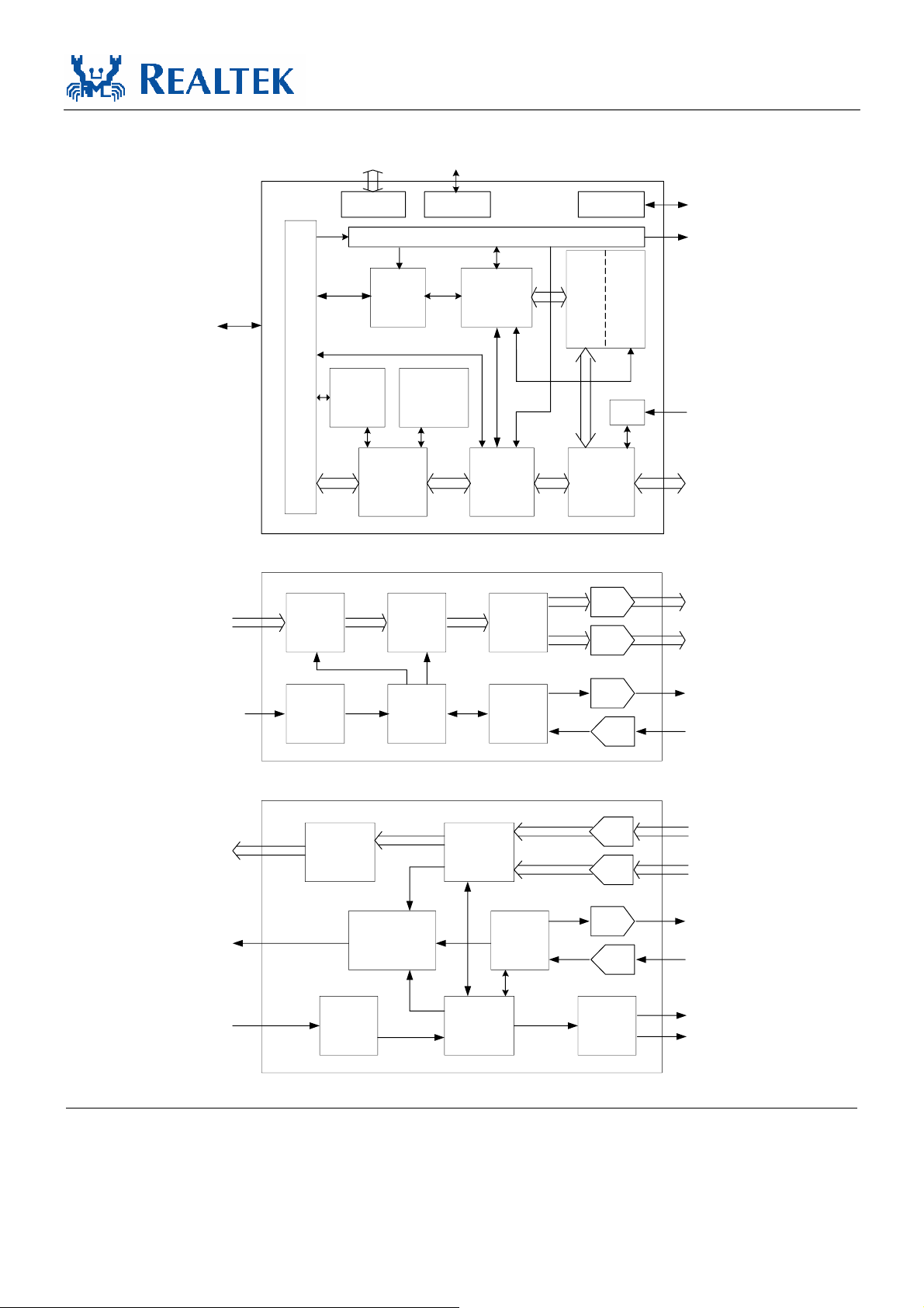
4. Block Diagrams
RTL8187SE
Datasheet
MAC
PCI
Express
Interface
BBP, TX Section
MAC/BBP
Interface
Register
Scrambler
EEPROM
Interface
LED Driver
Power and TX/RX Timing Control Logic
WEP/
TKIP/
AES
Engine
Interrupt
Control
Logic
FIFO
Coding
Checksum
Logic
RTS, CTS,
ACK Frame
Generator
FIFO
Control
Logic
Digital
Filter
Serial
Control
Register
Frame Length
Transmit/
Receive
Logic
Interface
DAC
DAC
Frame Type
CCA/
NAV
Radio and
Synthesizer
Control
Discriminator
From BBP
MAC/BBP
Interface
TXI
TXQ
From
MAC
Register
TX State
Machine
BBP, RX Section
MAC/BBP
Interface
To MAC
From
MAC
Single-Chip Wireless LAN Network Interface Controller
w/PCI Express Interface
Descrambler
Clear Channel
Signal Quality
Register
Assessment/
Figure 1. Block Diagram
Decoding
RX State
Machine
5
TX AGC
Control
RX AGC
Control
DAC
ADC
ADC
ADC
DAC
ADC
Antenna
Diversity
Control
TXAGC
TXDET
RXI
RXQ
RXAGC
RSSI
ANTSEL
ANTSELB
Track ID: JATR-1076-21 Rev. 1.0
RTL8187SE
Datasheet
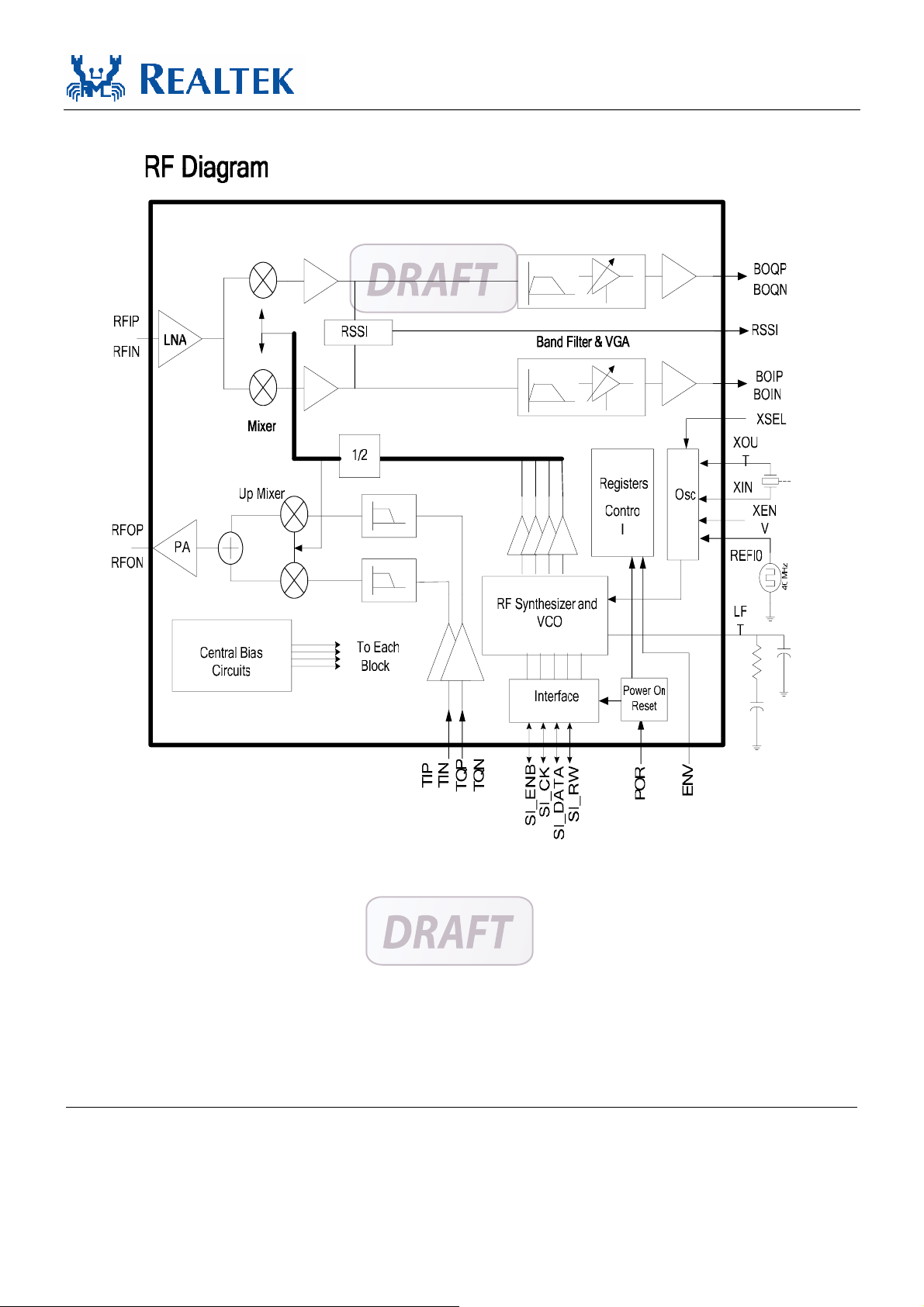
Figure 2. RF Block Diagram
Single-Chip Wireless LAN Network Interface Controller
w/PCI Express Interface
6
Track ID: JATR-1076-21 Rev. 1.0
5. Pin Assignments
RTL8187SE
Datasheet
DA8_DEBUG
TSSI
TRQP
TRQN
TRIN
TRIP
VAA33
R15K
AGND
VAA33
VAA33
XI
XO
VAA33
HSIP
HSIN
48 47 46 45 44 43 42 41 40 39 38 37 36 35 34 33
49
50
51
52
53
54
55
56
57
58
59
60
61
VDD
AGND
HSOP
LLLLLLL TXXXV
AGND
HSON
RTL8187SE
REFCLK-
REFCLK+
VDD
GND
LED1
PERSTB
WAKEB
CLKREQB
3
31
30
29
28
27
26
25
24
23
22
21
20
2
VDD33
GND
LED0
WLACT
BTSTAT
EECS
EESK/9356SEL
EEDI/AUX
EEDO
VDD
GND
VDD33
GND
VAA33
VD_CBC
VD_DIV
62
63
64
1 2 3 4 5 6 7 8 9
VAA33
65 GND (Exposed Pad)
RFIN
RFOP
VAA33
RFON
RFIP
Figure 3. Pin Assignments
PAPE
10 11 12 13 14 15 16
VDD
TRSWP
TRSWN
VAA33
VCTRL_LDO
GND
5.1. Package Identification
Green package is indicated by a ‘G’ in the location marked ‘T’ in Figure 3.
Single-Chip Wireless LAN Network Interface Controller
w/PCI Express Interface
7
19
18
7
1
EXTRSTB
ANTENSWN
ANTENSWP
Track ID: JATR-1076-21 Rev. 1.0
BTPRI
ISOLATEB
WLRXIND

RTL8187SE
Datasheet
6. Pin Descriptions
The following signal type codes are used in the tables:
I: Input AO: Analog Output
DI: Digital Input AIO: Analog Input/Output
AI: Analog Input T/S: Tri-State Bi-Directional Input/Output
O: Output S/T/S: Sustained Tri-State
DO: Digital Output O/D: Open Drain
6.1. Power Management/Isolation Interface
Table 1. Power Management/Isolation Interface
Symbol Type Pin No Description
WAKEB O/D 33 Power Management Event: Open drain, active low.
Used to reactivate the PCI Express slot’s main power rails and reference clocks.
ISOLATEB DI 18 Isolate Pin: Active low.
Used to isolate the RTL8187SE-GR from the PCI Express bus. The
RTL8187SE-GR will not drive its PCI Express outputs (excluding WAKEB) and
will not sample its PCI Express input as long as the Isolate pin is asserted.
6.2. PCI Express Interface
Table 2. PCI Express Interface
Symbol Type Pin No Description
REFCLK+ I 40
REFCLK- I 39
HSOP O 43
HSON O 42
HSIP I 47
HSIN I 46
PERSTB I 36 PCI Express Reset Signal: Active low.
CLKREQB O/D 34 Reference Clock Request Signal. This signal is used by the RTL8187SE-GR to
Single-Chip Wireless LAN Network Interface Controller
w/PCI Express Interface
PCI Express Differential Reference Clock Source: 100MHz ±300ppm.
PCI Express Transmit Differential Pair.
PCI Express Receive Differential Pair.
When the PERSTB is asserted at power-on state, the RTL8187SE-GR returns
to a pre-defined reset state and is ready for initialization and configuration
after the de-assertion of the PERSTB.
request starting of the PCI Express reference clock.
8
Track ID: JATR-1076-21 Rev. 1.0

RTL8187SE
Datasheet
6.3. EEPROM Interface
Table 3. EEPROM Interface
Symbol Type Pin No Description
EESK/9356SEL DO/DI 26 EESK in 93C46 (93C56) programming or auto-load mode.
Input Pin as 9356 Select Pin at Initial Power-up.
When this pin is pulled high with a 10K resistor, the 93C56 EEPROM
is used to store the resource data for the RTL8187SE.
The RTL8187SE latches the status of this pin at power-up to
determine which EEPROM (93C46 or 93C56) is used.
After power on and GPIO_EN[5]=1, this pin is GPIO[5].
EEDI/AUX DO/DI 25 EEDI: Output to serial data input pin of EEPROM.
AUX: Input pin to detect if Aux. Power exists or not on initial
power-on. This pin should be connected to EEPROM. To support
wakeup from ACPI D3cold or APM power-down, this pin must be
pulled high to Aux. Power via a resistor. If this pin is not pulled high to
Aux. Power, the RTL8187SE assumes that no Aux. Power exists.
After power on and GPIO_EN[4]=1, this pin is GPIO[4].
EEDO DI 24 This pin is GPIO[3] after power on and GPIO_EN[3]=1, otherwise, it
is EEDO in 93C46 (93C56) programming or auto-load mode.
EECS DO 27 EEPROM Chip Select.
93C46 (93C56) chip select.
6.4. Power Pins
Table 4. Power Pins
Symbol Type Pin No Description
VDD33 P 21, 32 +3.3V (Digital).
VAA33 P 1, 2, 11, 48, 55, 58, 59, 62+3.3V (Analog).
VDD P 12, 23, 37, 44 +1.8V.
GND P 13, 20, 22, 31, 38, 65 Ground (Digital).
AGND P 41, 45, 57 Ground (Analog).
VCTRL_LDO AO 10 Reserve this pin for external BJT option to generate 1.8V for digital
core circuit.
VD_CBC P 63 Reserved for external power transistor.
VD_DIV P 64 Reserved for external power transistor.
Single-Chip Wireless LAN Network Interface Controller
w/PCI Express Interface
9
Track ID: JATR-1076-21 Rev. 1.0

RTL8187SE
Datasheet
6.5. LED Interface
Table 5. LED Interface
Symbol Type Pin No Description
LED0 O 30 LED Pin.
a. PWRON: I2C_CK
b. After PWRON & LED_CONTROL=3’h7: GPIO[0]
c. Other: LED0
LED1 O 35 LED Pin.
a. PWRON: I2C_IO
b. After PWRON & LED_CONTROL=3’h7: GPIO[1]
c. Other: LED1
6.6. Baseband and RF Pins
Table 6. Baseband and RF Pins
Symbol Type Pin No Description
RFOP AO 3
RFON AO 4
RFIN AI 5
RFIP AI 6
PAPE DO 7 Enable Control for Optional External Power Amplifier
TRSWN DO 8
TRSWP DO 9
ANTENSWP DO 15
ANTENSWN DO 16
TSSI AI 50 Transmit Signal Strength Indication From External Power Amplifier
TRQP AIO 51 Via register setting, can be programmed to one of the following four types of pins:
TRQN AIO 52 Via register setting, can be programmed to one of the following four types of pins:
TRIN AIO 53 Via register setting, can be programmed to one of the following four types of pins:
TRIP AIO 54 Via register setting, can be programmed to one of the following four types of pins:
2.4GHz Differential RF Power Amplifier Output.
2.4GHz Differential RF Input.
Control Signals for Optional External RF T/R Switch
Control Signals for Antenna Switch
RF TXQP: Input pin for RF TX test RF RXQP: Output pin for RF RX test
AFE TXQP: Output pin for DAC test AFE RXQP: Input pin for ADC test
RF TXQN: Input pin for RF TX test RF RXQN: Output pin for RF RX test
AFE TXQN: Output pin for DAC test AFE RXQN: Input pin for ADC test
RF TXIN: Input pin for RF TX test RF RXIN: Output pin for RF RX test
AFE TXIN: Output pin for DAC test AFE RXIN: Input pin for ADC test
RF TXIP: Input pin for RF TX test RF RXIP: Output pin for RF RX test
AFE TXIP: Output pin for DAC test AFE RXIP: Input pin for ADC test
Single-Chip Wireless LAN Network Interface Controller
w/PCI Express Interface
10
Track ID: JATR-1076-21 Rev. 1.0

6.7. Bluetooth Co-Existence Pins
Table 7. Bluetooth Co-Existence Pins
Symbol Type Pin No Description
WLRXIND O 17 Wireless LAN RX Activity Indicator
BTPRI IO 19 Bluetooth Priority Pin
This pin is GPIO[2] after power on and GPIO_EN[2]=1, otherwise, this pin is
BTPRI. The BTPRI signal indicates when an important Bluetooth packet is being
transmitted or received.
BTSTAT IO 28 Bluetooth Status
This pin is GPIO[6] after power on and GPIO_EN[6]=1, otherwise, this pin is
BTSTAT. The BTSTAT signal indicates when normal Bluetooth packets are being
transmitted or received.
WLACT O 29 WLAN Activity
The WLAN_Active signal indicates when WLAN is either transmitting or
receiving in the 2.4GHz ISM band.
6.8. Clock and Other Pins
RTL8187SE
Datasheet
Table 8. Clock and Other Pins
Symbol Type Pin No Description
R15K IO 56 This pin must be pulled low by a 15K resistor.
XI I 60 Input of 40MHz Clock Reference.
XO O 61 Output of 40MHz Clock Reference.
EXTRSTB I 14 External Reset Pin: Active Low.
DA8_DEBUG O 49 Debug Pin.
7. EEPROM (93C46 or 93C56) Contents
The RTL8187SE supports the attachment of an external EEPROM. The 93C46 is a 1Kbit EEPROM
(the 93C56 is a 2Kbit EEPROM). The EEPROM interface provides the ability for the RTL8187SE to read
from, and write data to, an external serial EEPROM device. Values in the external EEPROM allow default
fields in PCI configuration space and IO space to be overridden following an internal power on reset, or
software EEPROM auto-load command. The RTL8187SE will auto-load values from the EEPROM to
these fields in configuration space and IO space. If the EEPROM is not present, the RTL8187SE
initialization uses default values for the appropriate Configuration and Operational Registers. Software can
read and write to the EEPROM using ‘bit-bang’ accesses via the 9346CR Register.
Note: It is suggested to obtain Realtek approval before changing the default settings of the EEPROM.
Single-Chip Wireless LAN Network Interface Controller
w/PCI Express Interface
11
Track ID: JATR-1076-21 Rev. 1.0
 Loading...