


RTL8208-VF
RTL8208-VF-LF
SINGLE-CHIP OCTAL 10/100MBPS FAST
ETHERNET TRANSCEIVER
DATASHEET
Rev. 1.0
24 March 2006
Track ID: JATR-1076-21
Realtek Semiconductor Corp.
No. 2, Innovation Road II, Hsinchu Science Park, Hsinchu 300, Taiwan
Tel.: +886-3-578-0211. Fax: +886-3-577-6047
www.realtek.com.tw

RTL8208-VF
Datasheet
COPYRIGHT
©2006 Realtek Semiconductor Corp. All rights reserved. No part of this document may be reproduced,
transmitted, transcribed, stored in a retrieval system, or translated into any language in any form or by any
means without the written permission of Realtek Semiconductor Corp.
DISCLAIMER
Realtek provides this document “as is”, without warranty of any kind, neither expressed nor implied,
including, but not limited to, the particular purpose. Realtek may make improvements and/or changes in
this document or in the product described in this document at any time. This document could include
technical inaccuracies or typographical errors.
TRADEMARKS
Realtek is a trademark of Realtek Semiconductor Corporation. Other names mentioned in this document are
trademarks/registered trademarks of their respective owners.
USING THIS DOCUMENT
This document is intended for the hardware and software engineer’s general information on the Realtek
RTL8208 Version ‘F’ IC.
Though every effort has been made to assure that this document is current and accurate, more information
may have become available subsequent to the production of this guide. In that event, please contact your
Realtek representative for additional information that may help in the development process.
REVISION HISTORY
Revision Release Date
1.0 2006/03/24 First release.
Summary
Single-Chip Octal 10/100Mbps Fast Ethernet Transceiver ii Track ID: JATR-1076-21 Rev. 1.0

RTL8208-VF
Datasheet
Table of Contents
1. General Description............................................................................................................................................................1
2. Features................................................................................................................................................................................1
3. Block Diagram.....................................................................................................................................................................2
4. Pin Assignments ..................................................................................................................................................................3
4.1. Package and Version Identification .............................................................................................................................3
5. Pin Descriptions ..................................................................................................................................................................5
5.1. Media Connection Pins ...............................................................................................................................................5
5.2. Power and Ground Pins...............................................................................................................................................5
5.3. Miscellaneous Pins......................................................................................................................................................6
5.4. RMII/SMII/SS-SMII Pins ...........................................................................................................................................7
5.5. SMI (Serial Management Interface) Pins....................................................................................................................8
5.6. LED Pins .....................................................................................................................................................................8
5.7. Mode Control Pins ......................................................................................................................................................8
5.8. Reserved Pins..............................................................................................................................................................9
6. Register Descriptions........................................................................................................................................................10
6.1. Register0: Control .....................................................................................................................................................10
6.2. Register1: Status........................................................................................................................................................12
6.3. Register2: PHY Identifier 1 Register.........................................................................................................................13
6.4. Register3: PHY Identifier 2 Register.........................................................................................................................13
6.5. Register4: Auto-Negotiation Advertisement .............................................................................................................14
6.6. Register5: Auto-Negotiation Link Partner Ability ..............................................................................................................15
6.7. Register6: Auto-Negotiation Expansion....................................................................................................................16
7. Functional Description .....................................................................................................................................................17
7.1. General......................................................................................................................................................................17
7.1.1. SMI (Serial Management Interface).....................................................................................................................17
7.1.2. Port Pair Loop Back Mode (PP-LPBK)................................................................................................................17
7.1.3. PHY Address ........................................................................................................................................................18
7.1.4. Auto-Negotiation..................................................................................................................................................18
7.1.5. Full-Duplex Flow Control ....................................................................................................................................18
7.2. Initialization and Setup..............................................................................................................................................18
7.2.1. Reset .....................................................................................................................................................................18
7.2.2. Setup and configuration........................................................................................................................................18
7.3. 10Base-T ...................................................................................................................................................................19
7.3.1. Transmit Function.................................................................................................................................................19
7.3.2. Receive Function..................................................................................................................................................19
7.3.3. Link Monitor ........................................................................................................................................................19
7.3.4. Jabber ...................................................................................................................................................................19
7.3.5. Loopback..............................................................................................................................................................19
7.4. 100Base-TX ..............................................................................................................................................................19
7.4.1. Transmit Function.................................................................................................................................................19
7.4.2. Receive Function..................................................................................................................................................20
7.4.3. Link Monitor ........................................................................................................................................................20
7.4.4. Baseline Wander Compensation ...........................................................................................................................21
7.5. 100Base-FX...............................................................................................................................................................21
7.5.1. Transmit Function.................................................................................................................................................21
7.5.2. Receive Function..................................................................................................................................................21
7.5.3. Link Monitor ........................................................................................................................................................22
7.5.4. Far-End-Fault-Indication (FEFI) ..........................................................................................................................22
7.5.5. Reduced Fiber Interface .......................................................................................................................................22
7.6. RMII/SMII/SS-SMII .................................................................................................................................................22
7.6.1. RMII (Reduced MII) ............................................................................................................................................23
7.6.2. SMII (Serial MII) .................................................................................................................................................23
Single-Chip Octal 10/100Mbps Fast Ethernet Transceiver iii Track ID: JATR-1076-21 Rev. 1.0

RTL8208-VF
Datasheet
7.6.3. SS-SMII (Source Synchronous -Serial MII)...............................................................................................................25
7.7. Power Saving and Power Down Mode......................................................................................................................26
7.7.1. Power Saving Mode .............................................................................................................................................26
7.7.2. Power Down Mode...............................................................................................................................................26
7.8. LED Configuration....................................................................................................................................................26
7.8.1. LED Blinking Time..............................................................................................................................................26
7.8.2. Serial Stream Order ..............................................................................................................................................27
7.8.3. Bi-Color LED.......................................................................................................................................................28
7.9. Crossover Detection and Auto Correction.................................................................................................................28
7.10. Polarity Detection and Auto Correction ....................................................................................................................29
7.11. 2.5V Power Generation.............................................................................................................................................29
8. Design and Layout Guide.................................................................................................................................................30
8.1. General Guidelines....................................................................................................................................................30
8.2. Differential Signal Layout Guidelines.......................................................................................................................30
8.3. Clock Circuit .............................................................................................................................................................30
8.4. 2.5V Power Considerations.......................................................................................................................................30
8.5. Power Planes .............................................................................................................................................................30
8.6. Ground Planes ...........................................................................................................................................................31
8.7. Transformer Options .................................................................................................................................................31
9. Application information ...................................................................................................................................................32
9.1. 10Base-T/100Base-TX Application ..........................................................................................................................32
9.2. 100Base-FX Application...........................................................................................................................................33
10. Electrical Characteristics ............................................................................................................................................34
10.1. Absolute Maximum Ratings......................................................................................................................................34
10.2. Operating Range........................................................................................................................................................34
10.3. DC Characteristics.....................................................................................................................................................34
10.4. AC Characteristics.....................................................................................................................................................35
10.5. Digital Timing Characteristics...................................................................................................................................36
10.6. Thermal Data.............................................................................................................................................................37
11. Mechanical Dimensions ...............................................................................................................................................38
11.1. Mechanical Dimensions Notes ..................................................................................................................................39
12. Ordering Information..................................................................................................................................................39
Single-Chip Octal 10/100Mbps Fast Ethernet Transceiver iv Track ID: JATR-1076-21 Rev. 1.0

RTL8208-VF
Datasheet
1. General Description
The RTL8208 Ve r sio n ‘ F’ is a highly integrated 8-port, 10Base-T/100Base-TX/FX, Ethernet transceiver
implemented in 0.25µm CMOS technology. It is currently the world’s smallest Octal-PHY chip package
with many special patented features. Traditional SD pins in 100Base-FX are omitted by Realtek patent to
obtain fewer pin-count. Flexible hardware settings are provided to configure the various operating modes of
the chip.
The RTL8208 consists of eight separate and independent channels. Each channel consists of an
RMII/SMII/SS-SMII interface to MAC controller. Hardware pins are used to configure the interface for
RMII, or SMII, or SS-SMII mode. In RMII mode, another hardware pin is used to set port-pair loop mode
(PP-LPBK mode), which can extend physical transmission length or perform physical media transport
operations without any switch controller. In addition, the RTL8208 features very low power consumption,
as low as 1.8 W (max.). Additionally, pin-outs designed to provide optimized direct routing may be
implemented, which simplifies layout work and reduces EMI noise issues.
2. Features
Supports 8-port integrated physical layer and
transceiver for 10Base-T and 100Base-TX
Up to 8 ports support 100Base-FX
Reduced 100Base-FX interface (patented)
Robust baseline wander correction for
improved 100Base-TX performance
Fully compliant with IEEE 802.3/802.3u
IEEE 802.3u compliant Auto-negotiation for
10/100 Mbps control
Hardware controlled Flow control
advertisement ability
Supports RMII/SMII/SS-SMII interfaces
Multiple driving capabilities of
RMII/SMII/SS-SMII
Supports 25MHz crystal as clock source for
RMII with 50MHz REFCLK output for MAC
Very low power consumption
Supports port-pair loop mode (PP-LPBK
mode)
Supports two Power reduction methods:
1. Power saving mode (cable detection)
2. Power down mode
Power-on auto-reset function eliminates the
need for external reset circuits
Crossover detection and auto correction.
Flexible LED display modes through 2-wire
serial
LED control interface
128-pin PQFP
2.5V/3.3V power supply
0.25µm, CMOS technology
Single-Chip Octal 10/100Mbps Fast Ethernet Transceiver 1 Track ID: JATR-1076-21 Rev. 1.0
RTL8208-VF
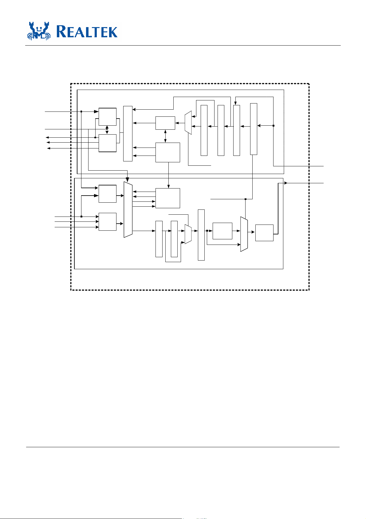
3. Block Diagram
SY NC
MODE[1:0]
RXD0
RXD1
CRSDV
TXD0
TXD1
TXEN
SM II
RX
RM II
RX
SM II
TX
RM II
TX
RX D[3:0]
RX FIFO
TX D[3:0]
CRS
RXDV
COL
TXCLK
TXEN
TXER
4B/5B
DECODE
RX
STA TE
MACHINE
TX
STA TE
MACHINE
4B/5B ENC ODE R
RX RECEIVE R
BYP-SCR
SCA MBL ER
RXCLK
EESCRAMBLER
BYP-DESCR
PARA LLEL -TO-SERIAL
SERIAL-TO-PARA LLEL
FX enable
MLT3
ENCODER
CLOCK RECOVERY
FX i nput
ADAPTIVE EQUALIZER
DRIVER
TP input
10/100
TX/FX
Datasheet
RX+/-
TX+/-
TX/FX output
TX TRANSMITTER
Single-Chip Octal 10/100Mbps Fast Ethernet Transceiver 2 Track ID: JATR-1076-21 Rev. 1.0
RTL8208-VF
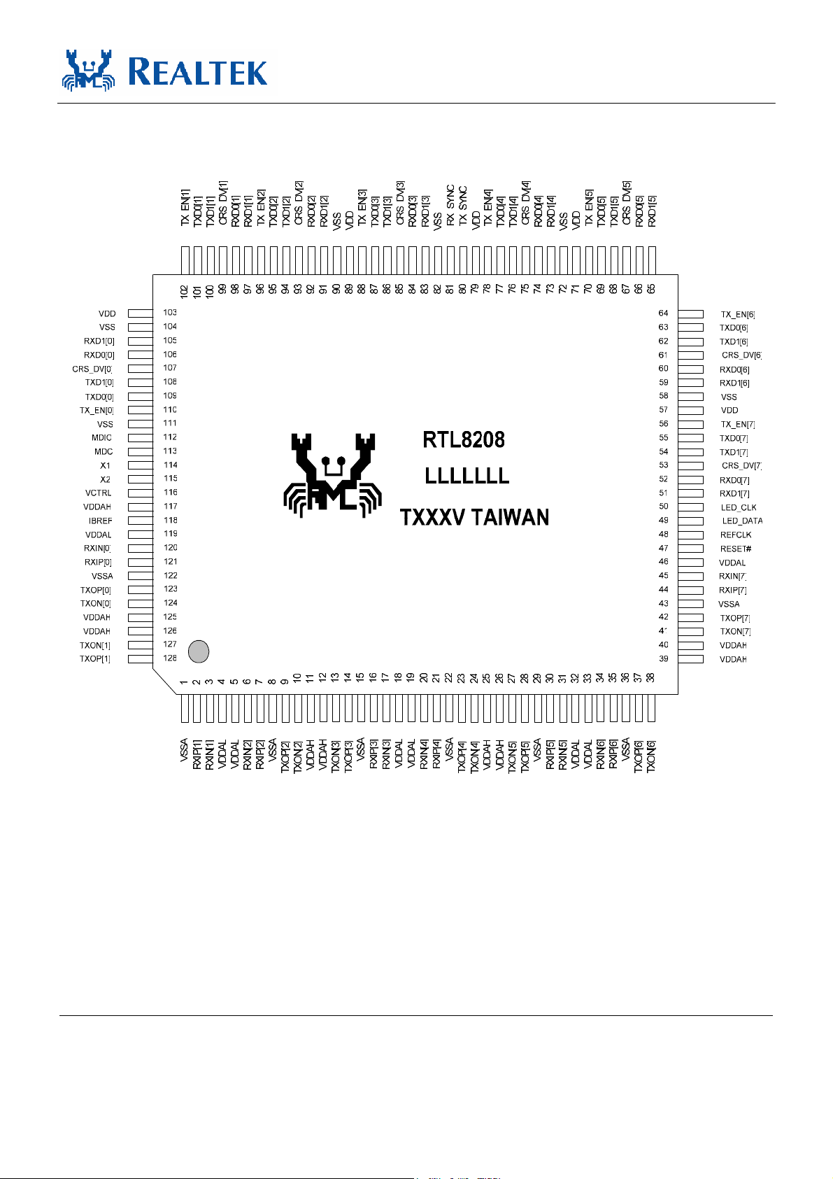
4. Pin Assignments
Datasheet
4.1. Package and Version Identification
Lead (Pb)-free package is indicated by an ‘L’ in the location marked ‘T’ in the figure above. The version
number is shown in the location marked ‘V’.
Single-Chip Octal 10/100Mbps Fast Ethernet Transceiver 3 Track ID: JATR-1076-21 Rev. 1.0

RTL8208-VF
'I' stands for input; 'O' stands for output; 'A' stands for analog; ‘D’ stands for digital
Pin Name Pin# Type Pin Name Pin# Type
VSSA
RXIP[1]
RXIN[1]
VDDAL
VDDAL
RXIN[2]
RXIP[2]
VSSA
TXOP[2]
TXON[2]
VDDAH
VDDAH
TXON[3]
TXOP[3]
VSSA
RXIP[3]
RXIN[3]
VDDAL
VDDAL
RXIN[4]
RXIP[4]
VSSA
TXOP[4]
TXON[4]
VDDAH
VDDAH
TXON[5]
TXOP[5]
VSSA
RXIP[5]
RXIN[5]
VDDAL
VDDAL
RXIN[6]
RXIP[6]
VSSA
TXOP[6]
TXON[6]
VDDAH
VDDAH
TXON[7]
TXOP[7]
VSSA
RXIP[7]
RXIN[7]
VDDAL
RESET#
REFCLK
LED_DATA/LEDMODE[1]
LED_CLK/LEDMODE[0]
RXD1[7]/EN_AUTOXOVER
RXD0[7]/DRIVE[0]
CRS_DV[7]/MODE[0]
TXD1[7]
TXD0[7]
TX_EN[7]
VDD
VSS
RXD1[6]/DISBLINK
RXD0[6]/DRIVE[1]
CRS_DV[6]/MODE[1]
TXD1[6]
TXD0[6]
TX_EN[6]
1
2
3
4
5
6
7
8
9
10
11
12
13
14
15
16
17
18
19
20
21
22
23
24
25
26
27
28
29
30
31
32
33
34
35
36
37
38
39
40
41
42
43
44
45
46
47
48
49
50
51
52
53
54
55
56
57
58
59
60
61
62
63
64
AGND
AI
AI
AVDD
AVDD
AI
AI
AGND
AO
AO
AVDD
AVDD
AO
AO
AGND
AI
AI
AVDD
AVDD
AI
AI
AGND
AO
AO
AVDD
AVDD
AO
AO
AGND
AI
AI
AVDD
AVDD
AI
AI
AGND
AO
AO
AVDD
AVDD
AO
AO
AGND
AI
AI
AVDD
I
I/O
I/O
I/O
I/O
I/O
I/O
I
I
I
DVDD
DGND
I/O
I/O
I/O
I
I
I
RXD1[5]/LED_BLNK_TIME
RXD0[5]
CRS_DV[5]/TP_PAUSE
TXD1[5]
TXD0[5]
TX_EN[5]
VDD
VSS
RXD1[4]/PHY_ADDR[4]
RXD0[4]
CRS_DV[4]/RX_CLK
TXD1[4]
TXD0[4]
TX_EN[4]/TX_CLK
VDD
SYNC/TX_SYNC
RX_SYNC/RPT_MODE
VSS
RXD1[3]/PHY_ADDR[3]
RXD0[3]
CRS_DV[3]/FX_PAUSE
TXD1[3]
TXD0[3]
TX_EN[3]
VDD
VSS
RXD1[2]/TEST
RXD0[2]
CRS_DV[2]/FX_DUPLEX
TXD1[2]
TXD0[2]
TX_EN[2]
RXD1[1]
RXD0[1]
CRS_DV[1]/SEL_TXFX[1]
TXD1[1]
TXD0[1]
TX_EN[1]
VDD
VSS
RXD1[0]
RXD0[0]
CRS_DV[0]/SEL_TXFX[0]
TXD1[0]
TXD0[0]
TX_EN[0]
VSS
MDIO
MDC
X1
X2
VCTRL
VDDAH
IBREF
VDDAL
RXIN[0]
RXIP[0]
VSSA
TXOP[0]
TXON[0]
VDDAH
VDDAH
TXON[1]
TXOP[1]
65
66
67
68
69
70
71
72
73
74
75
76
77
78
79
80
81
82
83
84
85
86
87
88
89
90
91
92
93
94
95
96
97
98
99
100
101
102
103
104
105
106
107
108
109
110
111
112
113
114
115
116
117
118
119
120
121
122
123
124
125
126
127
128
Datasheet
I/O
O
I/O
I
I
I
DVDD
DGND
I/O
O
O
I
I
I
DVDD
I
I/O
DGND
I/O
O
I/O
I
I
I
DVDD
DGND
I/O
O
I/O
I
I
I
O
O
I/O
I
I
I
DVDD
DGND
O
O
I/O
I
I
I
DGND
I/O
I
I
O
I/O
AVDD
AO
AVDD
AI
AI
AGND
AO
AO
AVDD
AVDD
AO
AO
Single-Chip Octal 10/100Mbps Fast Ethernet Transceiver 4 Track ID: JATR-1076-21 Rev. 1.0
RTL8208-VF
Datasheet
5. Pin Descriptions
In order to reduce pin count, and therefore size and cost, some pins have multiple functions. In those cases, the functions are
separated with a “/” symbol. Refer to the Pin Assignment diagram for a graphical representation.
'I' stands for input
'O' stands for output
'A' stands for analog signal
'D' stands for digital signal
'P' stands for power
'G' stands for ground
'Pu' stands for internal pull up (75K ohm)
'Pd' stands for internal pull down (75K ohm)
5.1. Media Connection Pins
Pin Name Pin Type Description
RXIP[7:0] 44,35,30,21,16,
7,2,121
RXIN[7:0] 45,34,31,20,17,
6,3,120
TXOP[7:0] 42,37,28,23,14,
9,128,123
TXON[7:0] 41,38,27,24,
13,10,127,124
AI Receiver Input: Differential positive signal shared by 100Base-TX,
100Base-FX, 10Base-T.
AI Receiver Input: Differential negative signal shared by 100Base-TX,
100Base-FX, 10Base-T.
AO Transmitter Output: Differential positive signal shared by
100Base-TX, 100Base-FX, 10Base-T.
AO Transmitter Output: Differential negative signal shared by
100Base-TX, 100Base-FX, 10Base-T.
5.2. Power and Ground Pins
Pin Name Pin Type Description
VDDAH 117 P
VDDAH 11,12,25,26,39,
40,125,126
VDDAL 119,4,5,18,19,
32,33,46
VSSA 122,1,8,15,22,
29,36,43
VDD 57,71,79,89,
103
VSS 58,72,82,90,
104,111
Power for IBREF
P 3.3V Power to analog: Used for transmitters and equalizers.
P 2.5V Power to analog: Used for PLL circuits.
G
Analog ground
P
Digital 2.5V power supply
G
Digital ground
Single-Chip Octal 10/100Mbps Fast Ethernet Transceiver 5 Track ID: JATR-1076-21 Rev. 1.0

RTL8208-VF
Datasheet
5.3. Miscellaneous Pins
Pin Name Pin Type Description
RESET# 47 I,
(Pu)
X1 114 I 25MHz Crystal X1 or 25MHz Oscillator clock input: When X1 is
X2 115 O
REFCLK 48 I/O
IBREF 118 A Reference Bias Resistor: This pin must be tied to analog ground through
VCTRL 116 O Voltage control: This pin controls a PNP transistor to generate the
Reset: This is an active low input. To complete the reset function, this
pin must be asserted low for at least 10ms.
pulled low, X2 must be floating. REFCLK will then be the chip clock
input.
25MHz Crystal X2
Reference clock:
If X1 is 25MHz active, REFCLK is a 50MHz output.
If X1 is pulled-low (disabled), REFCLK is the clock input as below:
50MHz 100ppm clock input for RMII mode.
125MHz 100ppm clock input for SMII/SS-SMII mode.
an external 1.96KΩ resistor when using a 1:1 transformer on Tx/Rx.
2.5V power supply for VDD and VDDAL pins.
Single-Chip Octal 10/100Mbps Fast Ethernet Transceiver 6 Track ID: JATR-1076-21 Rev. 1.0

RTL8208-VF
b
b
b
b
b
b
b
5.4. RMII/SMII/SS-SMII Pins
Pin Name Pin Type Description
TXD0[7:0] 55,63,69,77,
87,95,101,109
TXD1[7:0] 54,62,68,76,
86,94,100,108
TX_EN [7:0] 56,64,70,78,
88,96,102,110
RXD0[7:0] 52,60,66,74,
84,92,98,106
RXD1[7:0] 51,59,65,73,
83,91,97,105
CRS_DV[7:0] 53,61,67,75,
85,93,99,107
RX_CLK/
CRS_DV[4]
RX_SYNC
SYNC/
TX_SYNC
TX_CLK/
TX_EN[4]
75 O Receive Clock: In SS-SMII, CRS_DV[4] of RMII is used as
81 I/O
80 I Sync/Transmit Synchronous: In SMII, SYNC is a sync signal used
78 I Transmit Clock/Transmit Enable: In SS-SMII, TX_EN[4] of RMII
I
Transmit Data Input (bit 0):
In RMII, TXD0 and TXD1 are the di-bits input transmitted and driven
synchronously to REFCLK from MAC.
In SMII, TXD0 inputs the data that is transmitted and is driven
synchronously to REFCLK. In 100Mbps, TXD0 inputs a new 10segment starting with SYNC. In 10Mbps, TXD0 must repeat each
10-bit segment 10 times.
In SS-SMII, TXD0 behaves as SMII except synchronous to TX_CLK
instead of REFCLK and 10instead of SYNC.
I
Transmit Data Input (bit 1):
In RMII, TXD1 and TXD0 are the input di-bits synchronously to
REFCLK.
In SMII/SS-SMII, TXD1 is not used and should be tied either high or
low.
I
Transmit Enable:
In RMII , TX_EN indicates the disynchronous to REFCLK.
In SMII/SS-SMII, TX_EN[7:0] are not used.
O
Receive Data Input (bit 0):
In RMII, RXD0 and RXD1 output di-bits synchronously to REFCLK.
In SMII, RXD0 outputs data or inband management information
synchronously to REFCLK. In 100Mbps, RXD0 outputs a new 10segment starting with SYNC. In 10Mbps, RXD0 must repeat each
10-bit segment 10 times.
In SS-SMII, RXD0 behaves as SMII except synchronous to RX_CLK
instead of REFCLK and 10instead of SYNC.
O
Receive Data Input (bit 1):
In RMII, RXD1 and RXD0 output di-bits synchronously to REFCLK.
In SMII/SS-SMII, RXD1is not used and they are driven low.
O
Carrier Sense and Data Valid:
In RMII, CRS_DV is asynchronous to REFCLK and asserts when the
medium is non-idle.
In SMII/SS-SMII, CRS_DV[7:0] are not used and driven low.
RX_CLK, which is a 125MHz clock output.
Receive Synchronous :
In SS-SMII, RX_SYNC is a sync signal used to delimit the 10segment of RXD0 for all ports.
to delimit a 10-bit segment of RXD0 and TXD0 for all ports.
In SS-SMII, TX_SYNC is a sync signal used to delimit the 10segment of TXD0 for all ports.
is used as TX_CLK, which is a 125MHz clock input from MAC.
Datasheet
it
it segment starting with TX_SYNC
its on TXD is valid and is
it
it segment starting with RX_SYNC
it
it
Single-Chip Octal 10/100Mbps Fast Ethernet Transceiver 7 Track ID: JATR-1076-21 Rev. 1.0

RTL8208-VF
p
5.5. SMI (Serial Management Interface) Pins
Pin Name Pin Type Description
MDIO 112 I/O,
(Pu)
MDC 113 I,
(Pd)
Management Data I/O. Bi-directional data interface. A 1.5KΩ
pull-up resistor is required (as specified in IEEE802.3u).
The MAC controller access of the MII registers should be delayed at
least 700us after completion of the reset because of the internal reset
operation of the RTL8208-VF
Management Data Clock. 0 to 25MHz clock sourced by MAC to
sample MDIO.
The MAC controller access of the MII registers should be delayed at
least 700us after completion of the reset because of the internal reset
operation of the RTL8208-VF
5.6. LED Pins
Pin Name Pin Type Description
LED_DATA/
LEDMODE[1]
LED_CLK/
LEDMODE[0]
49 I/O LED_DATA outputs serial status bits that can be shifted into a shift
register to be displayed via LEDs. LED_DATA is output
synchronously to LED_CLK.
This pin is latched upon reset as LEDMODE[1]
LEDMODE[1:0] controls the forms of serial LED statuses.
See LED operation mode section.
50 I/O LED_CLK outputs the reference clock for the serial LED signals. This
pin is latched upon reset as LEDMODE[0]
Datasheet
5.7. Mode Control Pins
Pin Name Pin Type Description
SEL_TXFX[1:0]/
CRS_DV[1:0]
PP-LPBK mode
/ RX_SYNC
PHY_ADDR[4:3]/
RXD1[4:3]
MODE[1:0]/
CRS_DV[6:7]
TP_PAUSE/
CRS_DV[5]
99,107 I/O,
(Pd,Pd)
81 I/O,
(Pd)
73,83 I/O,
(Pd,Pu)
61,53 I/O,
(Pu,Pu)
67 I/O,
(Pu)
Select 10/100BaseTX or 100BaseFX: (default = 2’b00)
If RPT_MODE = 0:
2’b00: All 8 ports (port0~port7) are 10Base-T/100Base-TX.
2’b01: Port 7 is 100FX, other ports are 10Base-T/100Base-TX.
2’b10: Ports 6 & 7 are 100FX, other ports are 10Base-T/100Base-TX.
2’b11: All 8 ports are 100Base-FX.
If RPT_MODE =1:
2’b00: All 8 ports (port0~port7) are 10Base-T/100Base-TX.
2’b01: Port 7 and 5 are 100FX, others are 10Base-T/100Base-TX.
2’b10: Ports 1,3,5&7 are 100FX, others are 10Base-T/100Base-TX.
2’b11: All 8 ports are 100Base-FX.
Port Pair Loop Back mode: (default =0)
Upon power-on reset, this pin is input to assert PP-LPBK mode. When
set, all eight ports are portregeneration/transformation repeater.
Refer to the section covering PP-LPBK mode.
PHY Address: (default = 2’b01) These 2bits determine the highest
2bits of 5-bit PHY address upon reset.
Select RMII/SMII/SS-SMII mode: (default = 2’b11)
2’b1x: RMII
2’b00: SMII
2’b01: SS-SMII
Twisted Pair Pause capability: (default =1) Sets the Flow control
ability of Reg.4.10 for UTP ports upon power-on reset.
air looped back, acting like a signal
Single-Chip Octal 10/100Mbps Fast Ethernet Transceiver 8 Track ID: JATR-1076-21 Rev. 1.0

RTL8208-VF
Pin Name Pin Type Description
1: With flow control ability.
0: Without flow control ability
FX_PAUSE/
CRS_DV[3]
FX_DUPLEX/
CRS_DV[2]
EN_AUTOXOVER
/RXD1[7]
DISBLINK/
RXD1[6]
LED_BLNK_TIME/
RXD1[5]
LEDMODE[1:0] 49,50 I,
DRIVE[0]/
RXD0[7]
DRIVE[1]/
RXD0[6]
85 I/O,
(Pu)
93 I/O,
(Pu)
51 I/O,
(Pu)
59 I/O,
(Pd)
65 I/O,
(Pu)
(Pd,Pd)
52 I/O,
(Pd)
60 I/O,
(Pd,Pd)
100Base-FX Flow control capability: (default =1) Forces the flow
control capability of Reg.4.10 and Reg.5.10 upon power-on reset.
1: With flow control ability in 100Base-FX.
0: Without flow control ability in 100Base-FX.
FX_DUPLEX: Force 100Base-FX Full Duplex Mode: (default =1)
This pin sets 100Base-FX duplex and affects those ports in
100Base-FX mode.
1=full duplex, 0=half duplex.
Upon reset, this pin sets the default values of Reg.0.8 of those ports in
100Base-FX.
Enable Auto Crossover Detection: (default =1)
1: Enable auto crossover detection
0: Disable auto crossover detection
Disable power-on reset LEDs blinking: (default = 0)
1=Disable power-on LED blinking
0=blink.
LED blink time: (default =1) Used to control blinking speed of
activity and collision LEDs.
1= 43ms
0= 120ms
LEDMODE[1:0]: (default = 00) Controls the forms of serial LED status.
LEDMODE Mode Output
2’b00 3-bit serial stream Col/Fulldup, Link/Act, Spd
2’b01 2-bit serial stream Spd, Link/Act
2’b10 3-bit for Bi-color LED Col/Fulldup, Link/Act, Spd
See LED operation mode section for more information.
DRIVE[0]: Controls the output driving ability of SSMII RX_CLK.
1’b0: 12mA (default)
1’b1: 16mA
DRIVE[1]: Controls the output driving abilities of the
RMII/SMII/SS-SMII signals other than RX_CLK.
Drive [1:0] Output driving ability
2’b00 4mA (default)
2’b01 8mA
2’b10 12mA
2’b11 16mA
Datasheet
5.8. Reserved Pins
Pin Name Pin Type Description
ENANAPAR/
RXD1[1]
TEST/
RXD1[2]
CPRST/
RXD1[0]
Single-Chip Octal 10/100Mbps Fast Ethernet Transceiver 9 Track ID: JATR-1076-21 Rev. 1.0
97 I/O,
(Pd)
91 I/O,
(Pd)
105 I/O,
(Pd)
Reserved for internal use. Must be kept floating.
TEST. Reserved for internal use. Must be kept floating.
Reserved for internal use. Must be kept floating.

RTL8208-VF
Datasheet
6. Register Descriptions
The first six registers of the MII are defined by the MII specification. Other registers are defined by Realtek Semiconductor Corp.
for internal use and are reserved.
Register Description Default
0 Control Register 3100
1 Status Register 0F49
2 PHY Identifier 1 Register 001C
3 PHY Identifier 2 Register C883
4 Auto-Negotiation Advertisement Register 05E1
5 Auto-Negotiation Link Partner Ability Register 0001
6 Auto-Negotiation Expansion Register 0000
RO: Read Only
RW: Read/Write
LL: Latch Low until cleared
LH: Latch High until cleared
SC: Self Clearing
6.1. Register0: Control
Reg. bit Name Description Mode Default
0.15 Reset 1=PHY reset. This bit is self-clearing. RW/SC 0
0.14 Loopback This will loopback TXD to RXD and ignore all the activities on the
cable media. Valid only for 10Base-T.
1=Enable loopback.
0=Normal operation.
0.13 Spd_Sel When Nway is enabled, this bit reflects the result of
Auto-negotiation. (Read only)
When Nway is disabled, this bit can be set by SMI*. (Read/Write)
When 100FX is enabled, this bit =1 (Read only)
1=100Mbps.
0=10Mbps.
0.12 Auto Negotiation
Enable
0.11 Power Down 1=Power down. All functions will be disabled except
0.10 Isolate 1 = Electrically isolate the PHY from RMII/SMII/SS-SMII.
0.9 Restart Auto
Negotiation
0.8 Duplex Mode When Nway is enabled, this bit reflects the result of
0.[7:0] Reserved 0
*SMI: Serial Management Interface , which is composed of MDC,MDIO, allows MAC to manage PHY.
This bit can be set through SMI.(Read/Write)
When 100FX is enabled, this bit =0 (Read only)
1 = Enable Auto-negotiation process.
0 = disable Auto-negotiation process.
SMI.read/write function.
0=Normal operation.
PHY is still able to respond to MDC/MDIO.
0 = Normal operation
1=Restart Auto-Negotiation process.
0=Normal operation.
Auto-negotiation. (Read only)
When Nway is disabled, this bit can be set by SMI*. (Read/Write)
When 100FX is enabled, this bit is determined by the FX_DUPLEX
pin. (Read/Write)
1=Full duplex operation.
0=Half duplex operation.
RW 0
RW 1
RW 1
or
0 for 100FX
RW 0
RW 0
RW/SC 0
RW 1
Single-Chip Octal 10/100Mbps Fast Ethernet Transceiver 10 Track ID: JATR-1076-21 Rev. 1.0

RTL8208-VF
Datasheet
Reset – In order to reset the RTL8208 by software control, a ‘1’ must be written to bit 15 using an SMI write operation. The bit
clears itself after the reset process is complete, and does not need to be cleared using a second SMI write. Writes to other Control
register bits will have no effect until the reset process is completed, which requires approximately 1us. Writing a ‘0’ to this bit has
no effect. Because this bit is self clearing after a few cycles from a write operation, it will return a ‘0’ when read.
Loopback – The RTL8208 may be placed into loopback mode by writing a ‘1’ to bit 14. Loopback mode may be cleared either
by writing a ‘0’ to bit 14 or by resetting the chip. When this bit is read, it will return a ‘1’ when the chip is in software-controlled
loopback mode, otherwise it will return a ‘0’.
Speed Selection – If Auto-negotiation is enabled, this bit has no effect on the speed selection. However, if Auto-negotiation is
disabled by software control, the operating speed of the RTL8208 can be forced by writing the appropriate value to bit 13.
Writing a ‘1’ to this bit forces 100Base-X operation, while writing a ‘0’ forces 10Base-T operation. When this bit is read, it
returns the value of the software controlled forced speed selection only.
Auto Negotiation Enable – Default Auto Negotiation enable for all TP ports and disable for FX ports. Auto-negotiation can be
disabled by either software control to set 0.12=0.
Power Down – The RTL8208 supports a low power mode which is intended to decrease power consumption. Writing a ‘1’ will
enable power down mode, and writing a ‘0’ will return the RTL8208 to normal operation. When read, this register will return a
‘1’ when in power down mode, and a ‘0’ during normal operation.
Isolate – Each individual PHY may be isolated from its MII by writing a ‘1’ to bit 10. All MII outputs will be tri-stated and all
MII inputs will be ignored. Since the MII management interface is still active, the isolate mode may be cleared either by writing
a ‘0’ to bit 10 or by resetting the chip. When this bit is read, it will return a ‘1’ when the chip is in isolate mode, and a ‘0’ during
normal operation.
Restart Auto Negotiation – Bit 9 is a self-clearing bit that allows the Auto-negotiation process to be restarted, regardless of the
current status of the Auto-negotiation state machine. In order for this bit to have an effect, Auto-negotiation must be enabled.
Writing a ‘1’ to this bit restarts Auto-negotiation while writing a ‘0’ to this bit has no effect. When this bit is read, it will always
return a ‘0’.
Duplex Mode – By default, the RTL8208 powers up in half duplex mode. The chip can be forced into full duplex mode by
writing a ‘1’ to bit 8 while Auto-negotiation is disabled. Half duplex mode can be resumed either by writing a ‘0’ to bit 8 or by
resetting the chip. When Nway is enabled, this bit reflects the results of the Auto-negotiation, and is in a read only mode. When
Nway is disabled, this bit can be set through the SMI, and is in a read/write mode. When 100FX is enabled, this bit can be set
through the SMI or FX_DUPLEX pin and is in a read/write mode.
Reserved Bits – All reserved MII register bits must be written as ‘0’ at all times. Ignore the RTL8208 output when these bits are
read.
Single-Chip Octal 10/100Mbps Fast Ethernet Transceiver 11 Track ID: JATR-1076-21 Rev. 1.0

RTL8208-VF
b
Datasheet
6.2. Register1: Status
Reg. bit Name Description Mode Default
1.15 100Base_T4 0 = no 100Base-T4 capability. RO 0
1.14 100Base_TX_FD 1=100Base-TX full duplex capable.
0=Not 100Base-TX full duplex capable.
1.13 100Base_TX_HD 1=100Base-TX half duplex capable.
0=Not 100Base-TX half duplex capable.
1.12 10Base_T_FD 1=10Base-TX full duplex capable.
0=Not 10Base-TX full duplex capable.
1.11 10Base_T_HD 1=10Base-TX half duplex capable.
0=Not 10Base-TX half duplex capable.
1.[10:7] Reserved RO 0
1.6 MF Preamble
Suppression
1.5 Auto-negotiate
Complete
1.4 Remote Fault 1=Remote fault indication from link partner has been
1.3 Auto-Negotiation
Ability
1.2 Link Status 1=Link has never failed since previous read.
1.1 Jabber Detect 1=Jabber detected.
1.0 Extended Capability 1=Extended register capable (permanently =1)
100Base_T4 – The RTL8208 does not support the T4 function. Any reads to this bit will return a ‘0’.
100Base_TX_FD – The RTL8208 is capable of operating in 100Base-TX full duplex mode.
100Base_TX_HD – The RTL8208 is capable of operating in 100Base-TX half duplex mode.
10Base_T_FD – The RTL8208 is capable of operating in 10Base-T full duplex mode.
10Base_T_HD – The RTL8208 is capable of operating in 10Base-T half duplex mode.
Reserved – Ignore the output of the RTL8208 when these bits are read.
MF Preamble Suppression – Management Frame Preamble Suppression is permanently set in the RTL8208-VF, allowing
subsequent MII management frames to be accepted with or without the standard preamble pattern. Only two preamble bits are
required between successive management commands, instead of the normal 32, however, a minimum of 32 preamble bits are
required for the first SMI read/write transaction after reset. One idle bit is required between any two management transactions (as
defined in the IEEE802.3u spec). Reads of this bit will always return a ‘1’.
Auto-negotiate Complete – Bit 5 will return a ‘1’ if the Auto-negotiation process has been completed and the contents of
registers 4 and 5 are valid.
Remote Fault – When the link partner detects a far-end fault, it sends a far-end indication stream pattern. When the RTL8208
receives this pattern, it sets Reg1.4=1.
The RTL8208 will accept management frames with
preamble suppressed.
1=Auto-negotiation process completed. Reg.4,5 are valid if
this bit is set.
0=Auto-negotiation process not completed.
detected.
0=No remote fault indication detected.
When in 100FX mode, this bit means inFar-End-Fault is detected. Refer to FX MODE section.
1=NWay Auto-negotiation capable (permanently =1)
0=Without NWay Auto-negotiation capability
0=Link has failed since previous read.
If link fails, this bit will be set to 0 until bit is read.
0=No Jabber detected.
The jabber function is disabled in 100Base-X mode. Jabber
is supported only in 10Base-T mode.
0=Not extended register capable
and signal
RO 1
RO 1
RO 1
RO 1
RO 1
RO 0
RO/LH 0
RO 1
RO/LL 0
RO/LH 0
RO 1
Single-Chip Octal 10/100Mbps Fast Ethernet Transceiver 12 Track ID: JATR-1076-21 Rev. 1.0

RTL8208-VF
Datasheet
Auto-Negotiation Ability – The RTL8208 is capable of performing IEEE Auto-negotiation, and will return a ‘1’ when bit 4 is
read, regardless of whether or not the Auto-negotiation function has been disabled.
Link Status – The RTL8208 will return a ‘1’ on bit 2 when the link state machine is in Link Pass, indicating that a valid link has
been established. Otherwise, it will return ‘0’. When a link failure occurs after the link pass state has been entered, the Link Status
bit will be latched at ‘0’ and will remain so until the bit is read. After the bit is read, it becomes ‘1’ if the Link Pass state has been
entered again.
Jabber Detect – The RTL8208 will return a ‘1’ on bit 1 if a jabber condition has been detected. After the bit is read, or if the chip
is reset, it reverts to ‘0’. This is for 10Base-T only. Jabber occurs when a predefined excessive long packet is detected for
10Base-T. When the duration of TX_EN exceeds the jabber timer (21ms), the transmit and loopback functions will be disabled
and the COL LED starts blinking. After TX_EN goes low for more than 500 ms, the transmitter will be re-enabled and the COL
LED stops blinking.
Extended Capability – The RTL8208 supports extended capability registers, and will return a ‘1’ when bit 0 is read. Several
extended registers have been implemented in the RTL8208-VF.
6.3. Register2: PHY Identifier 1 Register
The PHY Identifier Registers #1 and #2 together form a unique identifier for the PHY section of this device. The Identifier
consists of a concatenation of the Organizationally Unique Identifier (OUI), the vendor's model number and the model revision
number. A PHY may return a value of zero in each of the 32 bits of the PHY Identifier if desired. The PHY Identifier is intended
to support network management.
Reg. bit Name Description Mode Default
2.[15:0] OUI Composed of the 3rd to 18th bits of the Organizationally
Unique Identifier (OUI), respectively.
RO 001C h
6.4. Register3: PHY Identifier 2 Register
Reg. bit Name Description Mode Default
3.[15:10] OUI Assigned to the 19th through 24th bits of the OUI. RO 110010
3.[9:4] Model Number Manufacturer's model number 08. RO 001000
3.[3:0] Revision Number Manufacturer's revision number 03. RO 0011
Single-Chip Octal 10/100Mbps Fast Ethernet Transceiver 13 Track ID: JATR-1076-21 Rev. 1.0

RTL8208-VF
Datasheet
6.5. Register4: Auto-Negotiation Advertisement
This register contains the advertisement abilities of this device as they will be transmitted to its Link Partner during
Auto-negotiation.
Reg. bit Name Description Mode Default
4.15 Next Page 1=Next Page enabled.
0=Next Page disabled. (Permanently =0)
4.14 Acknowledge Permanently =0. RO 0
4.13 Remote Fault 1=Advertises that RTL8208 has detected a remote fault.
0=No remote fault detected.
4.[12:11] Reserved RO 0
4.10 Pause 1=Advertises that the RTL8208 has flow control capability.
0=Without flow control capability.
In 100FX mode, this bit is set by 100FX_PAUSE upon reset.
In 100/10TP mode, this bit is set by TP_PAUSE upon reset.
4.9 100Base-T4 1 = 100Base-T4 capable.
0 = Not 100Base-T4 capable. (Permanently =0)
4.8
100Base-TX-FD
4.7 100Base-TX 1=100Base-TX half duplex capable.
4.6 10Base-T-FD 1=10Base-TX full duplex capable.
4.5 10Base-T 1=10Base-TX half duplex capable.
4.[4:0] Selector Field [00001]=IEEE802.3 RO 00001
Next Page – The RTL8208 does not implement the Next Page function, so bit 15 will always return a ‘0’ when read.
Acknowledge – Because the Next Page function is not implemented, bit 14 will always return a ‘0’ when read.
Remote Fault – When RTL8208 can not receive valid signal , set Reg4.13=1. The RTL8208 advertises this information to
inform link partner.
Reserved – Ignore the output of the RTL8208 when these bits are read.
Pause –Setting this bit indicates the availability of Flow Control capabilities when full duplex operation is in use. This bit is used
by one MAC to communicate Pause Capability to its Link Partner and has no effect on PHY operation.
100Base-T4 – Because the RTL8208 does not support the T4 function, any reads to this bit will return a ‘0’.
100Base-TX-FD – This bit advertises the ability to the Link Partner that the RTL8208 can operate in 100Base-TX full duplex
mode. Writing a ‘0’ to this bit will suppress the transmission of this ability to the Link Partner. Resetting the chip will restore the
default value. The default value is ‘1’ and writing a ‘1’ will set this bit to ‘1’. Reading this bit will return the last written value or
the default value if no write has been completed since the last reset.
100Base-TX – This bit advertises the ability to the Link Partner that the RTL8208 can operate in 100Base-TX half duplex mode.
Writing a ‘0’ to this bit will suppress the transmission of this ability to the Link Partner. Resetting the chip will restore the default
value. The default value is ‘1’ and writing a ‘1’ will set this bit to ‘1’. Reading this bit will return the last written value or the
default value if no write has been completed since the last reset.
10Base-T-FD – This bit advertises the ability to the Link Partner that the RTL8208 can operate in 10Base-T full duplex mode.
Writing a ‘0’ to this bit will suppress the transmission of this ability to the Link Partner. Resetting the chip will restore the default
value. The default value is ‘1’ and writing a ‘1’ will set this bit to ‘1’. Reading this bit will return the last written value or the
default value if no write has been completed since the last reset.
10Base-T – This bit advertises the ability to the Link Partner that the RTL8208 can operate in 10Base-T half duplex mode.
Writing a ‘0’ to this bit will suppress the transmission of this ability to the Link Partner. Resetting the chip will restore the default
value. The default value is ‘1’ and writing a ‘1’ will set this bit to ‘1’. Reading this bit will return the last written value or the
default value if no write has been completed since the last reset.
Selector Field – Bits 4:0 contain a fixed value of 00001, indicating that the chip belongs to the 802.3 class of PHY transceivers.
1=100Base-TX full duplex capable.
0=Not 100Base-TX full duplex capable.
0=Not 100Base-TX half duplex capable.
0=Not 10Base-TX full duplex capable.
0=Not 10Base-TX half duplex capable.
RO 0
RW 0
RW Set by
TP_PAUSE
Or
FX_PAUSE
RO 0
RW 1
RW 1
RW 1
RW 1
Single-Chip Octal 10/100Mbps Fast Ethernet Transceiver 14 Track ID: JATR-1076-21 Rev. 1.0

RTL8208-VF
Datasheet
6.6. Register5: Auto-Negotiation Link Partner Ability
This register contains the advertised abilities of the Link Partner as received during Auto-negotiation. The content changes after
the successful Auto-negotiation.
Reg. bit Name Description Mode Default
5.15 Next Page 1=Link partner desires Next Page transfer.
0=Link partner does not desire Next Page transfer.
5.14 Acknowledge 1=Link Partner acknowledges reception of FLP words.
0=No acknowledgement by Link Partner.
5.13 Remote Fault 1=Remote Fault indicated by Link Partner.
0=No remote fault indicated by Link Partner.
5.12-11 Reserved RO 0
5.10 Pause 1=Flow control supported by Link Partner.
0=No flow control supported by Link Partner.
When Nway is enabled, this bit reflects Link Partner ability. (read only)
In 100FX mode, this bit is set by FX_PAUSE or SMI.
5.9 100Base-T4 1=100Base-T4 supported by Link Partner.
0=100Base-T4 not supported by Link Partner.
5.8 100Base-TX-FD 1=100Base-TX full duplex supported by Link Partner.
0=100Base-TX full duplex not supported by Link Partner.
For 100FX mode, this bit is set when Reg.0.8=1 or
FX_DUPLEX =1.
When Nway is disabled, this bit is set when Reg.0.13=1 and
Reg.0.8=1.
5.7 100Base-TX 1=100Base-TX half duplex supported by Link Partner.
0=100Base-TX half duplex not supported by Link Partner.
For 100FX mode, this bit is set when Reg.0.8=0 or
FX_DUPLEX =0.
When Nway is disabled, this bit is set when Reg.0.13=1 and
Reg.0.8=0.
5.6 10Base-T-FD 1=10Base-TX full duplex supported by Link Partner.
0=10Base-TX full duplex not supported by Link Partner.
When Nway is disabled, this bit is set when Reg.0.13=0 and
Reg.0.8=1.
5.5 10Base-T 1=10Base-TX half duplex supported by Link Partner.
0=10Base-TX half duplex not supported by Link Partner.
When Nway disabled, this bit is set when Reg.0.13=0,and
Reg.0.8=0.
5.[4:0] Selector Field [00001]=IEEE802.3 RO 00001
Note that the values are only guaranteed to be valid once Auto-negotiation has successfully completed, as indicated by bit 5 of the
MII Status Register.
Next Page – Bit 15 returns a value of ‘1’ when the Link Partner implements the Next Page function and has Next Page
information that it wants to transmit. However, since the RTL8208 does not implement the Next Page function, it ignores the
Next Page bit, except to copy it to this register.
Acknowledge – Bit 14 is used by Auto-negotiation to indicate that a device has successfully received its Link Partner’s Link
Code Word.
Remote Fault – Bit 13 returns a value of ‘1’ when the Link Partner signals that it has detected a remote fault. The RTL8208
advertises this information, but does not act upon it.
Reserved – Ignore the output of the RTL8208 when these bits are read.
Pause – Indicates that the Link Partner pause bit is set.
100Base-T4 – Though the RTL8208 does not support the T4 function, this bit reflects this ability of the Link Partner.
RO 0
RO 0
RO 0
RW 0
RO 0
RO 0
RO 0
RO 0
RO 0
Single-Chip Octal 10/100Mbps Fast Ethernet Transceiver 15 Track ID: JATR-1076-21 Rev. 1.0

RTL8208-VF
Datasheet
100Base-TX-FD – This bit indicates that the Link Partner can support 100Base-TX full duplex mode. This bit is cleared any time
Auto-negotiation is restarted or the RTL8208 is reset.
100Base-TX – This bit indicates that the Link Partner can support 100Base-TX half duplex mode. This bit is cleared any time
Auto-negotiation is restarted or the RTL8208 is reset.
10Base-T-FD – This bit indicates that the Link Partner can support 10Base-T full duplex mode. This bit is cleared any time
Auto-negotiation is restarted or the RTL8208 is reset.
10Base-T – This bit indicates that the Link Partner can support 10Base-T half duplex mode. This bit is cleared any time
Auto-negotiation is restarted or the RTL8208 is reset.
Selector Field – Bits 4:0 reflect the value of the Link Partner’s selector field. These bits are cleared any time Auto-negotiation is
restarted or the chip is reset, and generally reflect the value of 0001, indicating that the Link Partner is an 802.3 device.
6.7. Register6: Auto-Negotiation Expansion
Reg. bit Name Description Mode Default
6.[15:5] Reserved RO 0
6.4 Parallel Detection
Fault
6.3 Link Partner Next
Page Able
6.2 Local Next Page
Able
6.1 Page Received 1= A New Page has been received.
6.0 Link Partner Auto-
Negotiation Able
Reserved – Ignore the output of the RTL8208 when these bits are read.
Parallel Detection Fault – Bit 4 is a read-only bit that gets latched high when a parallel detection fault occurs in the
Auto-negotiation state machine. For further details, please consult the IEEE standard. The bit is reset to ‘0’ after the register is
read, or when the chip is reset.
Link Partner Next Page Able – Bit 3 returns a ‘1’ when the Link Partner has Next Page capabilities. It has the same value as bit
15 of the Link Partner Ability Register.
Local Next Page Able – The RTL8208 does not have Next Page capabilities, so it will always return a ‘0’ when bit 2 is read.
Page Received – Bit 1 is latched high when a new link code word is received from the Link Partner, checked and acknowledged.
This bit is cleared when the link is lost or the chip is reset.
Link Partner Auto-Negotiation Able – Bit 0 returns a ‘1’ when the Link Partner is known to have Auto-negotiation capabilities.
Before any Auto-negotiation information is exchanged, or if the Link Partner does not comply with IEEE Auto-negotiation, the
bit returns a value of ‘0’.
1=A fault has been detected via the Parallel Detection function.
0=No fault has been detected via the Parallel Detection function.
1= Link Partner is Next Page able.
0= Link Partner is not Next Page able.
1= RTL8208 is Next Page able.
0= RTL8208 is not Next Page able. (permanently=0)
0= A New Page has not been received.
If Auto- Negotiation is enabled, this bit means:
1= Link Partner is Auto-Negotiation able.
0= Link Partner is not Auto-Negotiation able.
In 100FX or Nway disabled, this bit always =1.
RO 0
RO 0
RO 0
RO/LH 0
RO 0 (Auto-
Negotiation)
or
1 (100FX)
Single-Chip Octal 10/100Mbps Fast Ethernet Transceiver 16 Track ID: JATR-1076-21 Rev. 1.0

RTL8208-VF
Datasheet
7. Functional Description
7.1. General
7.1.1. SMI (Serial Management Interface)
SMI (Serial Management Interface) is also known as MII Management Interface, which consists of two signals, MDIO and MDC;
allowing the MAC controller to control and monitor the state of the PHY. MDC is a clock input for PHY to latch MDIO on its
rising edge. The clock can run from DC to 25MHz. MDIO is a bi-directional connection used to write data to, or read data from
PHY. The PHY address base is set by pins PHY_ADDR[4:3] and eight ports addresses of RTL8208 are internally
000,001,010,011,100,101,110,and 111.
SMI Read/Write Cycles
Preamble
(32 bits)
Read 1……..1 01 10 AAAAA RRRRR Z0 D…….D Z*
Write 1……..1 01 01 AAAAA RRRRR 10 D…….D Z*
*Z: high-impedance. During idle time, MDIO state is determined by an external 1.5KΩ pull-up resistor.
The RTL8208 supports Preamble Suppression, which allows the MAC to issue Read/Write Cycles without preamble bits (but
needs at least one Idle for every cycle). However, for the first MII management cycle after power-on reset, a 32-bit preamble is
needed. To guarantee the first successful SMI transaction after power-on reset, the MAC should be delayed at least 700us to issue
the first SMI Read/Write Cycle relative to the rising edge of reset.
Start
(2 bits)
OP Code
(2 bits)
PHYAD
(5 bits)
REGAD
(5 bits)
TurnAround
(2 bits)
Data
(16 bits)
Idle
7.1.2. Port Pair Loop Back Mode (PP-LPBK)
Port Pair Loop Back Mode (PP-LPBK) is enabled by pulling pin 81 high on reset. When in PP-LPBK mode, the ports of the
RTL8208 is configured as four pairs, port0 & port1, port2 & port3, port4 & port5, and port 6 & port7. Each pair are set as RMII
interface loop back, acting like a signal regeneration /transformation repeater, so a switch controller is not necessary.
In PP-LPBK mode, TP port and FX port selection is different from that in normal mode. The TP and FX port selection
configuration is as follows:
For this table, “U” means UTP port, “F” means Fiber port.
PP-LPBK
mode
(Pin 81)
0
(normal mode)
1
(PP-LPBK)
Since this configuration is a loopback mode, it uses full duplex only, and half duplex is not supported. The loopback-pair ports
should be configured to the same speed. Although this mode does not effect normal NWay mode, in order to keep the same speed
for each pair’s two ports, there is an auto-detection scheme. This scheme specifies that if one port of the pair is already linked,
when the other port is linked later, the earlier link-on port will re-start Auto-negotiation.
When PP-LPBK mode is set, there are three requirements: it must be based upon RMII mode; no switch controller is connected;
and TX_EN[7:0] is pulled down.
SEL_TXFX[1:0]
(Pin 99,107) Port0, Port1 Port2, Port3 Port4, Port5 Port6, Port7
0 0 U U U U U U U U
0 1 U U U U U U U F
1 0 U U U U U U F F
1 1 F F F F F F F F
0 0 U U U U U U U U
0 1 U U U U U F U F
1 0 U F U F U F U F
1 1 F F F F F F F F
Single-Chip Octal 10/100Mbps Fast Ethernet Transceiver 17 Track ID: JATR-1076-21 Rev. 1.0

RTL8208-VF
Datasheet
7.1.3. PHY Address
Each transceiver in the RTL8208 will have a unique PHY address for MII management. The address will be set through the PHY
address pins. The pins are latched at the trailing end of a reset. Transceiver 1 will have the address AA000, where AA=PHYAD
[4:3]. Each internal PHY address is AA000, AA001, AA010, AA011, AA100, AA101, AA110, AA111. Every time an SMI write
or read operation is executed, the transceiver compares the PHY address with its own PHY address definition, and the operation
is executed only when the addresses match.
7.1.4. Auto-Negotiation
For 10/100 TP port, the RTL8208 default setup is Auto-Negotiation enabled. Setting Register 0.12=0 by an SMI write can
disable Auto-Negotiation. For a 100FX port, Auto-Negotiation is always disabled.
For an Auto-Negotiation enabled port, the RTL8208 will negotiate with its link partner to determine the speed and duplex status.
The RTL8208-VF’s ability is advertised in Register 4, and , after Auto-Negotiation is finished, the link partner’s ability will be
stored in Register 5.
If the link partner is Auto-Negotiation disabled, the RTL8208 enters a parallel-detection state to identify the speed of the link
partner. The RTL8208 will link in the same speed as link partner, but in half duplex mode.
Auto-Negotiation is also used to determine Full-duplex flow control. flow control ability is advertised in Register 4.10. The link
partner’s flow control ability is stored in Register 5.10. See the following section for more information.
7.1.5. Full-Duplex Flow Control
If hardware pin TP_pause or 100FX_pause are enabled at power-on reset, Register 5.10=1 and Register 4.10=1. Therefore, after
reset is completed:
When Auto-Negotiation is enabled:
• Register 4.10 may be overwritten by the MAC
• Register 5.10 may be updated after NWay has completed
• Register 5.10 is set as read only for the MAC.
When Auto-Negotiation is disabled:
• Register 5.10 is set to R/W for the MAC through the SMI interface. If the SMI does not write to Register 5.10, it is still
Register 5.10=1, which means hardware forced flow control is enabled.
7.2. Initialization and Setup
7.2.1. Reset
The RTL8208 is initialized while in a reset state. During reset, each transceiver will be reset simultaneously. There are 3 ways to
reset the RTL8208-VF: Power-on auto reset; hardware pin reset; and software reset. The internal power-on auto reset circuit can
reset the chip while the reset pin (pin47) is floating. The hardware reset signal must be asserted to pin 47, RESET#, low for at
least 100ms. A software reset is implemented by writing Register 0.15=1, which is self clearing.
7.2.2. Setup and configuration
The operational modes of the RTL8208 can be configured either by hardware pin (pulled high or low) upon reset or by software
programming via accessing the RTL8208 registers through the SMI. Refer to the pin and register description sections.
Single-Chip Octal 10/100Mbps Fast Ethernet Transceiver 18 Track ID: JATR-1076-21 Rev. 1.0

RTL8208-VF
Datasheet
7.3. 10Base-T
7.3.1. Transmit Function
When TX_EN is active, TXD from RMII/SMII/SS-SMII is serialized, Manchester-encoded, and driven into the network medium
as a packet stream. An on-chip filtering and wave shaping circuit eliminates the need for external filtering. The transmit function
is disabled when the link has failed or when Auto-negotiation proceeds.
7.3.2. Receive Function
The Manchester decoder converts the incoming serial stream when the circuit detects the signal , and the digital serial stream is
then converted to 2-bit (RMII) or 1-bit (SMII/SS-SMII) data format. The preamble of the incoming stream is stripped off and
regenerated. SFD is generated into RXD once the incoming SFD is detected and data bits entering the elastic buffer are over
threshold.
7.3.3. Link Monitor
The 10Base-T link pulse detection circuit constantly monitors the RXIP/RXIN pins for the presence of valid link pulses.
Auto-polarity is implemented for correcting the detected reverse polarity of the RXIP/RXIN signal pairs.
7.3.4. Jabber
Jabber occurs when TX_EN is asserted over 21ms. Both transmit and loopback functions are disabled once jabber occurs. The
MII Register 1.1 (Jabber detect) bit is set high until jabber disappears and the bit is read again. The Jabber function is supported
in 10-Base-T only, and is not implemented in 100Base-TX. The collision LED of the corresponding port will blink while Jabber
occurs. Jabber is dismissed after TX_EN remains low for at least 500ms.
7.3.5. Loopback
Loopback mode can be achieved by writing to Register 0.14=1. Loopback mode routes transmitted data at the output of NRZ to
the NRZI conversion module, back to the receiving path. This mode is used to check all the device’s connection at the 5-bit
symbol bus, and verify the operation of the phase locked loop.
7.4. 100Base-TX
An internal 125MHz clock is generated by an on-chip PLL circuit to synchronize the transmit data or generate the clock signal for
the incoming data stream.
7.4.1. Transmit Function
Upon detection of TX_EN high, the RTL8208 converts RMII/SMII/SS-SMII TXD to 5 bit code-group and substitutes J/K
code-groups for the first 2 code-groups, which are called Start of Stream Delimiter (SSD). 4B5B coding continues for all of the data
as long as TX_EN is asserted high. At the end of TX_EN, T/R code-groups are appended to the last data field, which will be stripped
off at the remote receiving side. During the inter-packet gap, where TX_EN deasserted, IDLE code-groups are transmitted for the
sake of clocking of the remote receiver. The 5-bit serial data stream after 4B5B coding is then scrambled as defined by the TP-PMD
Stream Cipher function to flatten the power spectrum energy such that EMI effects can be significantly reduced.
This multi-level signaling technology moves the power spectrum energy from high frequency to low frequency, which also
benefits EMI emission. Scrambling is not implemented in 100Base-FX.
Single-Chip Octal 10/100Mbps Fast Ethernet Transceiver 19 Track ID: JATR-1076-21 Rev. 1.0

RTL8208-VF
Datasheet
7.4.2. Receive Function
The receive path includes a receiver composed of an adaptive equalizer and DC restoration circuits. These circuits compensate
for incoming distortion of the MLT-3 signal. An MLT-3 to NRZI, and NRZI to NRZ converter is used to convert analog signals to
digital bit-streams. A PLL circuit is also included to clock data bits exactly with minimum bit error rate. De-scrambler, 5B/4B
decoder and serial-to-parallel conversion circuits follow. CRS_DV is asserted no later than when the SSD
(Start-of-Stream-Delimiter) is detected within a few bits time (delay due to the elastic buffer as mentioned in the RMII section),
and ends toggling once the data in the elastic buffer has been dumped to RXD.
Name 4B Code 5B Code Definition
0 0000 11110 Data 0
1 0001 01001 Data 1
2 0010 10100 Data 2
3 0011 10101 Data 3
4 0100 01010 Data 4
5 0101 01011 Data 5
6 0110 01110 Data 6
7 0111 01111 Data 7
8 1000 10010 Data 8
9 1001 10011 Data 9
A 1010 10110 Data A
B 1011 10111 Data B
C 1100 11010 Data C
D 1101 11011 Data D
E 1110 11100 Data E
F 1111 11101 Data F
I 0000* 11111 Idle
J 0101* 11000 Start of stream Delimiter, Part 1
K 0101* 10001 Start of stream Delimiter, Part 2
T 0000* 01101 End of stream Delimiter, Part 1
R 0000* 00111 End of stream Delimiter, Part 2
H 1000 00100 Transmit Error (used to force signaling errors)
V 0111 00000 Invalid code
V 0111 00001 Invalid code
V 0111 00010 Invalid code
V 0111 00011 Invalid code
V 0111 00101 Invalid code
V 0111 00110 Invalid code
V 0111 01000 Invalid code
V 0111 01100 Invalid code
V 0111 10000 Invalid code
V 0111 11001 Invalid code
*Treated as an invalid code (mapped to 0111) when received in data field.
4B5B Encoding
7.4.3. Link Monitor
In 100Base-TX mode, receive signal energy is detected by monitoring the receive pair for transitions in the signal level. Signal
levels are qualified using squelch detect circuits. When no signal or valid signals are detected on the receive pair, the link
monitor will enter and remain in the “Link Fail” state where only idle codes will be transmitted. When a valid signal is
detected on the receive pair for a minimum period of time, the link monitor will enter the “Link Pass” state and the transmit
and receive functions will be enabled.
Single-Chip Octal 10/100Mbps Fast Ethernet Transceiver 20 Track ID: JATR-1076-21 Rev. 1.0

RTL8208-VF
Datasheet
7.4.4. Baseline Wander Compensation
The RTL8208 is ANSI TP-PMD compliant and supports input and Base Line Wander (BLW) compensation in 100Base-TX
mode. The RTL8208 does not require external attenuation circuitry at its receive inputs, RXIP/RXIN. It accepts TP-PMD
compliant waveforms directly, requiring only a 100Ω termination and a 1:1 transformer.
BLW is the change in the average DC content, over time, of an AC coupled digital transmission over a given transmission
medium. BLW is a result from the interaction between the low frequency components of a transmitted bit stream and the
frequency response of the AC coupling component(s) within the transmission system. If the low frequency content of the digital
bit stream goes below the low frequency pole of the AC coupling transformers, then the droop characteristics of the transformers
will dominate resulting in potentially serious BLW. If BLW is not compensated for, packet loss will occur.
7.5. 100Base-FX
The RTL8208 can be configured into 100Base-FX mode through SEL_TXFX[1:0] (RPT_MODE should be 0). According to the
setting of SEL_TXFX[1:0], port 7 or port 6/7 or all eight ports can be configured to 100Base-FX operation.
Medium type RPT_MODE=0
SEL_TXFX[1:0]
2’b00 UTP UTP UTP UTP UTP UTP UTP UTP
2’b01 UTP UTP UTP UTP UTP UTP UTP FX
2’b10 UTP UTP UTP UTP UTP UTP FX FX
2’b11 FX FX FX FX FX FX FX FX
UTP: 10Base-T/100Base-TX,
FX: 100Base-FX.
Compared to common 100Base-FX applications, the RTL8208 lacks a pair of differential SD (signal detect) signals to achieve
its link monitoring function (patent), which significantly reduces the pin count in this octal PHY.
Port 0 Port 1 Port2 Port3 Port4 Port5 Port6 Port7
Any of the RTL8208 transceivers may interface with an external 100Base-FX fiber optic device and receiver instead of the
magnetics module used with twisted pair cable. The differential transmit and receive data pairs will operate at PECL voltage
levels instead of those required for twisted-pair transmission. The data will be encoded using two-level NRZI instead of
three-level MLT3. The data stream is not scrambled for fiber-optic transmission.
7.5.1. Transmit Function
In 100Base-FX transmission, TXD is processed as 100Base-TX, except without scrambling, before the NRZI stage. Instead of
converting to MLT-3 signals, as in 100Base-TX, the serial data stream is driven out as NRZI PECL signals, which enter the fiber
transceiver in differential-pairs form. The fiber transceiver should be available working in a 3.3V environment. Refer to the fiber
application section for more information.
PECL DC characteristics
Parameter Symbol Min Max Unit
PECL Input High Voltage Vih Vdd-1.16 Vdd-0.88 V
PECL Input Low Voltage Vil Vdd-1.81 Vdd-1.47 V
PECL Output High Voltage Voh Vdd-1.02 V
PECL Output Low Voltage Vol Vdd-1.62 V
7.5.2. Receive Function
Signals are received through PECL receiver inputs from the fiber transceiver, and directly passed to the clock recovery circuit for
data/clock recovery. The scrambler/descrambler is bypassed in 100Base-FX mode.
Single-Chip Octal 10/100Mbps Fast Ethernet Transceiver 21 Track ID: JATR-1076-21 Rev. 1.0

RTL8208-VF
Datasheet
7.5.3. Link Monitor
In 100Base-FX mode, if the RTL8208 receive path detects a valid link word, it enters the link state. If no valid link word is
detected, it is in a link down state. Therefore, SD+/- is not necessary. The RTL8208 uses a reduced 100Base-FX interface.
7.5.4. Far-End-Fault-Indication (FEFI)
The MII Register 1.4 (Remote Fault indication detected) is a FEFI bit when 100FX is enabled, which indicates FEFI has been
detected. FEFI is an alternative in-band signaling method which is composed of 84 consecutive ‘1’ followed by one ‘0’. From the
point of view of the RTL8208-VF, once this pattern is detected 3 times, Register 1.4 is set, which means the transmit path
(Remote side’s receive path) has some problems.
On the other hand, if the RTL8208 detects no valid link pulse on RxOP/N pair, it sends out a FEFI stream pattern, which in turn
will cause the remote side to detect a Far-End-Fault indication. This means the RTL8208 sees problems on the receive path.
The FEFI mechanism is used only in 100Base-FX applications.
7.5.5. Reduced Fiber Interface
The.RTL8208 ignores the underlying SD signal of the fiber transceiver to complete link detection and connection. This is
achieved by monitoring RD signals from the fiber transceiver and checking if any link integrity events are met. This significantly
reduces pin-count, especially for high-port PHY devices. This is a Realtek patent-pending technology and available only with
Realtek product solutions.
7.6. RMII/SMII/SS-SMII
The interface to the MAC can be RMII, SMII, or SS-SMII through MODE[1:0]. When floating MODE[1:0] upon power-on reset,
the RTL8208 operates in RMII mode (default).
MODE[1:0] Operation Mode REFCLK Clock Input
2’b1x RMII 50MHz, 100ppm
2’b00 SMII 125MHz, 100ppm
2’b01 SS-SMII 125MHz, 100ppm
Below illustrates the signals required for each interface:
RMII SMII SS-SMII
REFCLK REFCLK REFCLK
SYNC TX_SYNC
RX_SYNC
CRS_DV[3:0]
CRS_DV[4] RX_CLK
CRS_DV[7:5]
RXD0[7:0] RXD0[7:0] RXD0[7:0]
RXD1[7:0]
TX_EN[3:0]
TX_EN[4] TX_CLK
TX_EN[7:5]
TXD0[7:0] TXD0[7:0] TXD0[7:0]
TXD1[7:0]
Single-Chip Octal 10/100Mbps Fast Ethernet Transceiver 22 Track ID: JATR-1076-21 Rev. 1.0

RTL8208-VF
Datasheet
7.6.1. RMII (Reduced MII)
The RTL8208 meets all of the RMII requirements outlined in the RMII Consortium specifications. The main advantage
introduced by RMII is pin count reduction; e.g., it operates with only one 50Mhz reference clock for both the TX and RX sides
without separate clocks needed for both paths, as with the MII interface. However, some hardware modification is needed for this
change, the most important and outstanding of which is the presence of an elastic buffer for absorption of the frequency
difference between the 50MHz reference clock and the clocking information of the incoming data stream. Another change
implemented is that the MII RXDV and Carrier_Sense are merged into one signal, CRS_DV, which is asserted high while
detecting incoming packet data. When internal Carrier_Sense de-asserted, CRS_DV is de-asserted when the first di-bit of a
nibble is presented onto RXD[1:0] synchronously to REFCLK. If there is still data in the FIFO that has not yet been presented
onto RXD[1:0], then on the second di-bit of a nibble CRS_DV reasserts. This pattern of assertion and de-assertion continues until
all received data in the FIFO has been presented onto RXD[1:0]
RTL 8208-V F
X1
CRS_DV[7:0]
RXD0[7:0]
RXD1[7:0]
TX_EN[7:0]
TXD0[7:0]
TXD1[7:0]
REFCLK
8-port
MAC
RTL 8208-V F
X1
X2
25M H z
CRS_DV[7:0]
RXD0[7:0]
RXD1[7:0]
TX_EN[7:0]
TXD0[7:0]
TXD1[7:0]
REFCLK
8-port
MAC
50MHz
oscillator
RMII Signal Diagram RMII Signal Diagram
50MHz Oscillator Solution 25MHz Crystal Solution
7.6.2. SMII (Serial MII)
The RTL8208 also supports SMII interface to MAC, which allows a further reduction in the number of signals. As illustrated
below, both the MAC and RTL8208 are synchronous to a 125MHz reference clock.
SYNC
TXD0[7:0]
8-port
MAC
X1
oscillator
RXD0[7:0]
REFCLK
125MHz
SMII Signal Diagram
RTL8208-VF
Single-Chip Octal 10/100Mbps Fast Ethernet Transceiver 23 Track ID: JATR-1076-21 Rev. 1.0

RTL8208-VF
Datasheet
Receive Path
Receive data and control information are signaled in 10-bit segments. SYNC signal is used to delimit the 10-bit segments. MAC
is responsible to generate these SYNC pulses every ten clocks. For 100Mbps mode, each segment represents a byte of data.
However, for 10Mbps mode, each segment is repeated ten times to represent a byte of data. The receive sequence contains all of
the information defined on the standard MII receive path.
CRS
X0
X1
REFCLK
SYNC
RXD[0]
RXD0 RXD1
RXER from
previous
frame
0 =10Mbps
1 =100Mbps
Speed
RXD2
Duplex
0 = Half
1 = Full
One Data Byte (Two MII Data Nibbles)
RXD3 RXD4 RXD5 RXD6
Link
0 = Down
1 = Up
Jabber
0 = OK
1 = Detected
Upper Nibble
0 = Invalid
1 = Valid
SMII Reception Encoding
1 2 3 4 5 6 7 8 9 10
CRS RXDV RXD0 RXD7RXD6RXD5RXD4RXD3RXD2RXD1
SMII Reception
False Carrier
0 = OK
1 = Detected
RXD7RX_DV
1
Transmit Path
Transmit data and control information are signaled in 10-bit segments. SYNC signal is used to delimit the 10-bit segments. MAC
is responsible to generate these SYNC pulses every ten clocks. For 100Mbps mode, each segment represents a byte of data.
However, for 10Mbps mode, each segment is repeated ten times to represent a byte of data.
TXD0 TXD1 TXD2 TXD3 TXD4 TXD5 TXD6 TXD7TXENTXER
TXD0 TXD1 TXD2 TXD3 TXD4 TXD5 TXD6 TXD7TXENTXER
TXD0 TXD1 TXD2 TXD3 TXD4 TXD5 TXD6 TXD7TXENTXER
0
0
XX
0
X
1
X
X
X
X
XXXX
XXXX
XXXX
One Data Byte (Two MII Data Nibbles)
One Data Byte (Two MII Data Nibbles)
One Data Byte (Two MII Data Nibbles)
X
X
SMII Transmission Encoding
1 2 3 4 5 6 7 8 9 10
1 2 3 4 5 6 7 8 9 10
1 2 3 4 5 6 7 8 9 10
REFCLK
REFCLK
REFCLK
SYNC
SYNC
SYNC
TX_ER TX_EN TXD0 TXD7TXD6TXD5TXD4TXD3TXD2TXD1
TX_ER TX_EN TXD0 TXD7TXD6TXD5TXD4TXD3TXD2TXD1
TX_ER TX_EN TXD0 TXD7TXD6TXD5TXD4TXD3TXD2TXD1
SMII Transmission
Collision Detection
The RTL8208 does not indicate that a collision has occurred. It is left up to the MAC to detect the assertion of both CRS_DV and
TX_EN.
Single-Chip Octal 10/100Mbps Fast Ethernet Transceiver 24 Track ID: JATR-1076-21 Rev. 1.0

RTL8208-VF
Datasheet
7.6.3. SS-SMII (Source Synchronous -Serial MII)
Source-Synchronous SMII is designed for applications requiring a trace delay of more than 1ns. Three signals are added to the
SMII interface: RX_SYNC, RX_CLK, TX_CLK; and the SYNC of SMII is modified to TX_SYNC in SS-SMII.
TX_SYNC
TXD0[7:0]
TX_CLK
8-port
MAC
X1
125MHz
oscillator
SS-SMII Signal Diagram
Receive Path
Receive data and control information are signaled in 10-bit segments. RX_SYNC signal is used to delimit the 10-bit segments.
RTL8208 is responsible to generate these RX_SYNC pulses every ten clocks. For 100Mbps mode, each segment represents a
byte of data. However, for 10Mbps mode, each segment is repeated ten times to represent a byte of data. The receive sequence
contains all of the information defined on the standard MII receive path.
1 2 3 4 5 6 7 8 9 10
RX_SYNC
RXD0[7:0]
RX_CLK
REFCLK
RTL8208-VF
RX_CLK
RX_SYNC
RXD[0]
CRS RXDV RXD0 RXD7RXD6RXD5RXD4RXD3RXD2RXD1
SS-SMII Reception
Transmit Path
Transmit data and control information are signaled in 10-bit segments. The TX_SYNC signal is used to delimit the 10-bit
segments. The MAC is responsible for generating these TX_SYNC pulses every ten clocks. For 100Mbps mode, each segment
represents a byte of data. However, for 10Mbps mode, each segment is repeated ten times to represent a byte of data. The receive
sequence contains all of the information defined on the standard MII receive path. The PHY can sample one of the ten segments.
1 2 3 4 5 6 7 8 9 10
TX_CLK
TX_SYNC
TXD[0]
TX_ER TX_EN TXD0 TXD7TXD6TXD5TXD4TXD3TXD2TXD1
SS-SMII Transmission
Collision Detection
The RTL8208 does not indicate that a collision has occurred. It is left up to the MAC to detect the assertion of both CRS_DV and
TX_EN.
Single-Chip Octal 10/100Mbps Fast Ethernet Transceiver 25 Track ID: JATR-1076-21 Rev. 1.0

RTL8208-VF
Datasheet
7.7. Power Saving and Power Down Mode
7.7.1. Power Saving Mode
The RTL8208 implements a power saving mode on a per-port basis. A port automatically enters power saving mode 10 seconds
after the cable is disconnected from it, regardless of whether the RTL8208-VF’s operation mode is NWay or Forced mode. Once
the port enters power saving mode, it transmits normal link pulses only on its TXOP/TXON pins, and keeps monitoring
RXIP/RXIN to detect any incoming signals, which might be a 100Base-TX MLT-3 idle pattern, 10Base-T link pulses or NWay’s
FLP (fast link pulses). After it detects incoming signals, it wakes up from the power saving mode and operates in normal mode
according to the result of the connection negotiation.
Power saving mode is not supported when in 100FX operation.
7.7.2. Power Down Mode
Setting Register 0.11through the SMI interface forces the corresponding port of the RTL8208 to enter power down mode, which
disables all transmit/receive functions and RMII functions on that port, except SMI (MDC/MDIO management interface).
7.8. LED Configuration
The RTL8208 supports serial LED status streams for LED display. The forms of LED status streams, as shown below, are
controlled by LEDMODE[1:0] pins, which are latched upon reset. All LED statuses are represented as active-low, except
Link/Act in Bi-color LED mode, whose polarity depends on Spd status.
LEDMODE[1:0] Mode Output Sequences
00 3-bit serial stream Col/Fulldup, Link/Act, Spd
01 2-bit serial stream Spd, Link/Act
10 3-bit for Bi-color LED Col/Fulldup, Link/Act, Spd
LED Statuses Description
Col/Fulldup Col, Full duplex Indicator. Blinking every 43ms when collision
happens. Low for full duplex, and high for half duplex mode.
Link/Act Link, Activity Indicator. For 3-bit serial stream mode, low for link
established. For 3-bit Bi-color LED mode, Link/Act is high for
link established when speed is low (100Mb/s); Link/Act is low for
link established when speed is high (10Mb/s). Link/Act Blinks
every 43ms when the corresponding port is transmitting or
receiving.
Spd Speed Indicator. Low for 100Mb/s, and high for 10Mb/s.
7.8.1. LED Blinking Time
LED blinking time can be set to 120ms by setting LED_BLNK_TIME=0. The LED status’s supporting 43/120ms blinking time
are Col/Fulldup, Link/Act. For status Link/Act/Spd, the LED blinking time is not affected by LED_BLNK_TIME.
Single-Chip Octal 10/100Mbps Fast Ethernet Transceiver 26 Track ID: JATR-1076-21 Rev. 1.0

RTL8208-VF
Datasheet
7.8.2. Serial Stream Order
Every bit stream is output port by port, from port0 to port7 with Col/Fulldup as the first bit in a port stream. For 2-bit serial stream
mode, the sequence is Spd, then Link/Act. The following diagrams illustrate the sequences in 3-bit and 2-bit serial stream mode.
2.56 us2.56 us2.56 us
242322212019
SpdCol/Dup Link/Act
LEDCLK
LEDDTA
LEDCLK
LEDDTA
2.56 us 2.56 us 2.56 us 2.56 us2.56 us 2.56 us
31 2
Link/Act SpdCol/Dup
Port 0 3-bit serial stream
Link/Act SpdCol/Dup
3-Bit Serial Stream Mode
2.56 us 2.56 us 2.56 us 2.56 us2.56 us 2.56 us
1 2
Link/ActSpd
Port 0 2-bit
serial stream
Link/ActSpd
Port 6 2-bit
serial stream
2-Bit Serial Stream Mode
Spd
Port 7 2-bit
serial stream
Port 7 3-bit serial streamPort 6 3-bit serial stream
2.56 us
16151413
Link/Act
LEDDTA
LEDCLK
VDD
VDD
VDD
VDD
A
CLK
B
CLR
A
CLK
B
CLR
A
CLK
B
CLR
74164
74164
74164
QA
QB
QC
QD
QE
QF
QG
QH
QA
QB
QC
QD
QE
QF
QG
QH
QA
QB
QC
QD
QE
QF
QG
QH
port 7 Spd LED
port 7 Link/Act LED
port 7 Col/Dup LED
port 6 Spd LED
port 6 Link/Act LED
port 6 Col/Dup LED
port 5 Spd LED
port 5 Link/Act LED
port 5 Col/Dup LED
port 4 Spd LED
port 4 Link/Act LED
port 4 Col/Dup LED
port 3 Spd LED
port 3 Link/Act LED
port 3 Col/Dup LED
port 2 Spd LED
port 2 Link/Act LED
port 2 Col/Dup LED
port 1 Spd LED
port 1 Link/Act LED
port 1 Col/Dup LED
port 0 Spd LED
port 0 Link/Act LED
port 0 Col/Dup LED
External circuit for 3-bit serial LED mode
Single-Chip Octal 10/100Mbps Fast Ethernet Transceiver 27 Track ID: JATR-1076-21 Rev. 1.0

RTL8208-VF
74164
74164
QA
QB
QC
QD
QE
QF
QG
QH
QA
QB
QC
QD
QE
QF
QG
QH
LEDDTA
LEDCLK
A
CLK
VDD
B
CLR
A
CLK
VDD
B
CLR
External circuit for 2-bit serial LED mode
VDD
port 7 Link/Act LED
port 7 Spd LED
port 6 Link/Act LED
port 6 Spd LED
port 5 Link/Act LED
port 5 Spd LED
port 4 Link/Act LED
port 4 Spd LED
port 3 Link/Act LED
port 3 Spd LED
port 2 Link/Act LED
port 2 Spd LED
port 1 Link/Act LED
port 1 Spd LED
port 0 Link/Act LED
port 0 Spd LED
Datasheet
7.8.3. Bi-Color LED
For 3-bit Bi-color LED mode, Link/Act and Spd are used for one Bi-color LED package, which is a single LED package with
two LEDs connected in parallel with opposite polarities.
Yellow
Spd Link/Act Indication Bi-Color State
0 0 No Link Off
0 1 100Mb/s Link up Green
Spd
Link/Act
1 0 10Mb/s Link up Yellow
Green
7.9. Crossover Detection and Auto Correction
During the link setup phase, the RTL8208 checks for reception of active signals on every port to determine if a connection can be
established. If the receive data pin pair is connected to receive pin pair of the peer device (and vice versa), the RTL8208 will
automatically change its configuration to swap receive data pins with transmit data pins. In other words, the RTL8208 can adapt
automatically to a peer device's configuration. If a port is connected to a PC or NIC with an MDI-X interface with a crossover
cable, the RTL8208 will reconfigure the port to provide an MDI-X interface to ensure a proper connection. This will effectively
replace the eight-DIP switch commonly used for reconfiguring a port on a hub or switch.
By pulling-up EN_AUTOXOVER, the RTL8208 can identify the type of connected cable to adjust its port as for MDI or MDIX
operation. When switching to MDI mode, the RTL8208 uses TXOP/N as transmit pairs, and when switching to MDIX mode, the
RTL8208 uses RXIP/N as transmit pairs. The same is true for the receive pairs. This function is port-based implemented.
Pulling-down EN_AUTOXOVER will disable this function and the RTL8208 operates in MDI mode, in which TXOP/N
represents transmit pairs and RXIP/N represents receive pairs.
Single-Chip Octal 10/100Mbps Fast Ethernet Transceiver 28 Track ID: JATR-1076-21 Rev. 1.0

RTL8208-VF
Datasheet
7.10. Polarity Detection and Auto Correction
For better noise immunity and lower interference to ambient devices, the Ethernet electrical signal on a twisted pair cable is
transmitted in differential forms. That is, the signal is transmitted on two wires for each direction with inverse polarities (+/-). If
wiring on the connector is faulty or a faulty transformer is used, the two inputs to a transceiver may carry signals with opposite
but incorrect polarities. As a direct consequence, the transceiver will not work properly.
When the RTL8208 operates in 10Base-T mode, it automatically reverses the polarity of its two receiver input pins if it detects
that the polarities of the incoming signals on the pins are incorrect. However, this feature is unnecessary when the RTL8208 is
operating in 100Base-TX mode.
7.11. 2.5V Power Generation
The RTL8208 uses a PNP transistor to generate 2.5V from the 3.3V power supply. This 2.5V provides for digital core and analog
receive circuits. Once your system needs more than one RTL8208 chip (greater than 8 ports), do not use one PNP transistor for all
of the RTL8208 chips even if the rating is enough. Instead, use one transistor for each RTL8208-VF.
Do not connect any beads directly between the collector of PNP transistor and VDDAL. This will affect the stability of the 2.5V
power significantly if the bead exists.
3.3V
3.3V
VDDAH
VDDAH: 3.3V
RTL8208-VF
2SB1197
K
Ic(max.)=800mA
2.5V
47uF
Using a PNP Transistor to Produce 2.5V
The power transistor is a 2SB1197K, and follows the following specifications.
Absolute maximum ratings (Ta=25°C)
Parameter Symbol Limits Unit
Collector-base voltage VCBO -40 V
Collector-emitter voltage VCEO -32 V
Emitter-base voltage VEBO -5 V
Collector current IC -0.8 A(DC)
Collector power dissipation PC 0.2 W
Junction temperature Tj 150
Storage temperature Tstg -55~+150
For more information, refer to http://www.rohm.com
VCTRL
VDDAL
0.1uF
°C
°C
VDDAL: 2.5V
Single-Chip Octal 10/100Mbps Fast Ethernet Transceiver 29 Track ID: JATR-1076-21 Rev. 1.0

RTL8208-VF
Datasheet
8. Design and Layout Guide
In order to achieve maximum performance for the RTL8208-VF, good design attention is required throughout the design and
layout process. The following recommendations can help to implement a high performance system.
8.1. General Guidelines
• Create a good power source, minimizing noise from switching power supply circuits.
• Verify the quality of the components, such as clock source and transformer, to meet the application requirements.
• Keep power and ground noise levels below 150mV.
• Use bulk capacitors (4.7uF-10uF) between the power and ground planes.
• Use 0.1uF decoupling capacitors to reduce high-frequency noise on the power and ground planes.
• Keep decoupling capacitors as close as possible to the RTL8208 power pins.
• Provide termination for all TXOP/N and RXIP/N.
8.2. Differential Signal Layout Guidelines
• Keep differential pairs as close as possible and route both traces as identically as possible.
• Avoid vias and layer changes if possible.
• Keep the different pairs away from each other.
8.3. Clock Circuit
• The clock should be 25M/50MHz/125MHz 100ppm with jitter less than 0.5ns.
• If use 50MHz or 125MHz as clock source, make the length of clock path to RTL8208 equal to the length to MAC as possible.
The length difference should be under 1 inch.
• If use 50MHz, please put a damping resistor at clock source side.
• If possible, make clock trace smooth, strait, and surrounded by ground traces to minimize high-frequency emissions.
8.4. 2.5V Power Considerations
• Do not connect a bead directly between the collector of the PNP transistor and VDDAL. This will affect the stability of the 2.5V
power significantly.
• Use a bulk of capacitor (4.7uF-10uF) between the collector of PNP transistor and ground plane.
• Do not use one PNP transistor for more than one RTL8208 chip, even if the rating is enough. Use one transistor for each
RTL8208-VF.
8.5. Power Planes
• If the layout board size is small, it is better not to divide the power plane into digital and analog power planes.
• Use 0.1uF decoupling capacitors and bulk capacitors between power plane and ground plane.
Single-Chip Octal 10/100Mbps Fast Ethernet Transceiver 30 Track ID: JATR-1076-21 Rev. 1.0

RTL8208-VF
Datasheet
8.6. Ground Planes
• If the layout board size is small, keep the system ground region as one continuous, unbroken plane.
• Place a moat (gap) between the system ground and chassis ground.
• For better ESD test performance, please use iron case, and put screw to connect frame ground to iron case.
8.7. Transformer Options
• Magnetics that support a 1:1 turn ratio on both the transmit and receive paths are required for the RTL8208-VF. There are many
vendors improving their magnetics design to meet this requirement, and several are listed below.
Vend or Model Ve nd or Model
Pulse H1164 BothHand 40ST1041AX
Magnetic 1 ML164 GTS FC-638L
• The center-tap of the primary side of the transformer should not be connected to ground with capacitors, because of the
RTL8208-VF’s special design.
Single-Chip Octal 10/100Mbps Fast Ethernet Transceiver 31 Track ID: JATR-1076-21 Rev. 1.0

RTL8208-VF
9. Application information
9.1. 10Base-T/100Base-TX Application
RXIP
RXIN
RTL8208-VF
TXOP
TXON
IBRE F
50Ω
1%
50Ω
1%
50Ω
1%
50Ω
1%
0.1uF
0.1uF
1.96ΚΩ, 1%
Pulse H1164
1:1
1:1
75Ω ∗ 3
0.1uF/3KV
1
2
3
4
5
6
7
8
RJ45
Datasheet
Chasis GND
10Base-T/100Base-TX Diagram
The Central Tap in the primary side of the H1164 must be left floating, and cannot be bypassed to GND via a capacitor.
Single-Chip Octal 10/100Mbps Fast Ethernet Transceiver 32 Track ID: JATR-1076-21 Rev. 1.0

RTL8208-VF
9.2. 100Base-FX Application
(3.3V Fiber Transceiver)
RXIP
RXIN
RTL8208-VF
VCC_TX (3.3V)
82 Ω
TXON
82 Ω
TXOP
130 Ω
130 Ω
VCC_RX (3.3V)
82Ω
130Ω
82Ω
82Ω
130Ω
VCC_RX (3.3V)
VCC_TX (3.3V)
DELTA
OPT-155A 2H1
1*9 SC Duplex FDDI
Fast Ethernet Optical
Transceiver Module
GND_RX
1
RD+
2
RD
3
-
SD
4
5
VCC_RX
VCC_TX
6
7
TD-
TD+
8
GND_TX
9
Datasheet
IBREF
1.96ΚΩ, 1%
Chasis GND
100Base-FX Application (3.3V Fiber Transceiver)
Single-Chip Octal 10/100Mbps Fast Ethernet Transceiver 33 Track ID: JATR-1076-21 Rev. 1.0

RTL8208-VF
Datasheet
10. Electrical Characteristics
10.1. Absolute Maximum Ratings
WA R N IN G : Absolute maximum ratings are limits beyond which permanent damage may be caused to the device or which may
affect device reliability. All voltages are specified reference to GND unless otherwise specified.
Parameter Minimum Maximum Units
Storage Temperature -10 +125
VDDAH Supply Referenced to GND GND-0.3 +3.63 V
VDDAL and VDD
Supply Referenced to GND
Digital Input Voltage GND-0.3 +3.6 V
GND-0.3 +2.75
10.2. Operating Range
Parameter Minimum Maximum Units
Ambient Operating Temperature(Ta) 0 +65
3.3V Supply Voltage Range (VDDAH) 3.15 3.45 V
2.5V Supply Voltage Range (VDDAL,VDD) 2.375 2.625 V
10.3. DC Characteristics
Parameter Symbol Conditions Min
Power Supply Current for
2.5V
Power Supply Current for
3.3V
Total Power Consumption
for all 8 ports
TTL Input High Voltage
TTL Input Low Voltage
TTL Input Current
TTL Input Capacitance
Output High Voltage
Output Low voltage
Icc 10 Base-T, idle
10 Base-T, Peak continuous 100% utilization
100 Base-TX, idle
100 Base-TX, Peak continuous 100% utilization
Power saving
Power down
Icc 10 Base-T, idle
10 Base-T, Peak continuous 100% utilization
100 Base-TX, idle
100 Base-TX, Peak continuous 100% utilization
Power saving
Power down
PS 10 Base-T, idle
10 Base-T, Peak continuous 100% utilization
100 Base-TX, idle
100 Base-TX, Peak continuous 100% utilization
Power saving
Power down
Vih
Vil
Iin
-10 10 µA
Cin
Voh
2.25 2.75 V
Vol
0 0.25 V
1.5 V
1.0 V
3 pF
Typi cal
81.2
88.9
125.5
145.7
76.7
15.5
88.5
499.2
370.7
371.3
48.1
495
1870
1537
1590
°C
V
°C
Max Units
mA
mA
3.3
mW
350
50
Single-Chip Octal 10/100Mbps Fast Ethernet Transceiver 34 Track ID: JATR-1076-21 Rev. 1.0

RTL8208-VF
Datasheet
Parameter SYM Conditions Min
Output Tristate Leakage
Current
TX+/- Output Current High
TX+/- Output Current Low
TX+/- Output Current High
TX+/- Output Current Low
RX+/- Common-mode input
voltage
RX+/- Differential input
resistance
Differential Input Resistance
Input Squelch Threshold 340 mV
10 uA
|IOZ|
Transmitter, 100Base-TX (1:1 Transformer Ratio)
IOH
IOL
Transmitter, 10Base-T(1:1 Transformer Ratio)
IOH
IOL
Receiver, 100Base-TX
Receiver, 10BaseT
20 mA
0 uA
50 mA
0 uA
1.6 V
20
20
Typi cal
Max Units
10.4. AC Characteristics
Parameter SYM Conditions Min
Transmitter, 100Base-TX
Differential Output Voltage,
peak-to-peak
Differential Output Voltage
Symmetry
Differential Output
Overshoot
Rise/Fall time
Rise/Fall time imbalance
Duty Cycle Distortion Deviation from best-fit time-grid, 010101 …
Timing jitter Idle pattern 870 ps
Differential Output Voltage,
peak-to-peak
TP_IDL Silence Duration Period of time from start of TP_IDL to link
TD Short Circuit Fault
Tolerance
TD Differential Output
Impedance (return loss)
TD Common-Mode Output
Voltage
Transmitter Output Jitter 7.6 ns
RD Differential Output
Impedance (return loss)
Harmonic Content dB below fundamental, 20 cycles of all ones data 29 dB
Start-of-idle Pulse width TP_IDL width ns
VOD
VOS
VOO
tr ,tf
|tr - tf|
VOD
Ecm
50Ω from each output to Vcc, Best-fit over 14 bit
times
50Ω from each output to Vcc, |Vp+|/|Vp-|
Percent of Vp+ or Vp- 3.9 %
10-90% of Vp+ or Vp- 4.0/4.0 ns
0 ps
Sequence
Transmitter, 10Base-T
50Ω from each output to Vcc, all pattern
pulses or period of time between link pulses
Peak output current on TD short circuit for 10
seconds.
Return loss from 5MHz to 10MHz for reference
resistance of 100 Ω.
Terminate each end with 50Ω resistive load.
Return loss from 5MHz to 10MHz for reference
resistance of 100Ω.
10.5 15.75 ms
12.4 25.5 dB
14 25 dB
Typi cal
1.986 V
98.7 %
4.27 V
199 mA
44 mV
±150
Max Units
ps
kΩ
kΩ
Single-Chip Octal 10/100Mbps Fast Ethernet Transceiver 35 Track ID: JATR-1076-21 Rev. 1.0

RTL8208-VF
Datasheet
10.5. Digital Timing Characteristics
Parameter SYM Conditions Min
100Base-TX Transmit System Timing
Active TX_EN Sampled to
first bit of “J on MDI output
Inactive TX_EN Sampled to
first bit of “T on MDI output
TX Propagation Delay
First bit of “J on MDI input
to CRS_DV assert
First bit of “T on MDI input
to CRS_DV de-assert
RX Propagation Delay
TX Propagation Delay
TX_EN to MDI output From TX_EN assert to TXOP/N 5 6 Bits
Carrier Sense Turn-on delay
Carrier Sense Turn-off
Delay
RX Propagation Delay
LED On Time
LED Off Time
Jabber Active From TX_EN=1 to Jabber asserted 60 70 80 ms
Jabber de-assert From TX_EN=0 to Jabber de-asserted 60 80 ms
TXD, TX_EN Setup time TXD [1:0], TX_EN to REFCLK rising edge
TXD, TX_EN Hold time TXD [1:0], TX_EN to REFCLK rising edge hold
RXD, CRSDV, RXER to
REFCLK delay
TXD, SYNC Setup time TXD, SYNC to REFCLK rising edge setup time 2 ns
TXD, SYNC Hold time TXD SYNC to REFCLK rising edge hold time 2 ns
RXD, to REFCLK delay Output delay from REFCLK rising edge to RXD 2.5 3.5 ns
MDC MDC clock rate 25 MHz
MDIO Setup Time Write cycle 10 ns
MDIO Hold Time Write cycle 10 ns
MDIO output delay relative
to rising edge of MDC
11 12 Bits
15 16 Bits
t
TXpd
t
RXpd
t
TXpd
t
CSON
t
CSOFF
t
RXpd
t
LEDon
t
LEDoff
From TXD[1:0] to TXOP/N 11 12 Bits
100Base-TX Receive System Timing
From RXIP/N to CRS_DV 6 8 Bits
From RXIP/N to CRS_DV 16 18 Bits
From RXIP/N to RXD[1:0] 15 17 Bits
10Base-T Transmit System Timing
From TXD[1:0] to TXOP/N 5 6 Bits
10Base-T Receive System Timing
Preamble on RXIP/N to CRS_DV asserted 12 Bits
TP_IDL to CRS_DV de-asserted 8 9 Bits
From RXIP/N to RXD[1:0] 9 12 Bits
LED timing
While LED blinking 43 120 ms
While LED blinking 43 120 ms
Jabber timing (10Base-T only)
RMII Timing
2 ns
setup time
2 ns
time
Output delay from REFCLK rising edge to RXD
[1:0], CRSDV, RXER
SMII Timing
SMI Timing
Read cycle 10 ns
4 ns
Typi cal
Max Units
Single-Chip Octal 10/100Mbps Fast Ethernet Transceiver 36 Track ID: JATR-1076-21 Rev. 1.0

RTL8208-VF
Datasheet
10.6. Thermal Data
Heat generated by the chip causes a temperature rise of the package. If the temperature of the chip (Tj, junction temperature) is
beyond the design, there will be negative effects on operation and the life of IC package. It’s necessary to develop a switch with
a reasonable environment (Ta, ambient temperature) in a closed case to achieve a stable and reliable system, via supporting
sufficient heat dissipation capability either through heat sink or electrical fan. However, to estimate the possible Ta is necessary
since as the power density increases, the thermal management is getting more critical.
Thermal parameters are defined as below according to JEDEC standard JESD 51-2, 51-6:
1. θja( Thermal resistance from junction to ambient), represents the resistance to the heat flows from the chip to ambient air.
It’s an index of heat dissipation capability. Lower θja means better thermal performance.
θja = (Tj - Ta) / Ph
Where Tj is the junction temperature
Ta is the ambient temperature
Ph is the power dissipation
2. θjc (Thermal resistance from junction to case), represents the resistance to the heat flows from the chip to package top case.
θjc is important when external heat sink is attached on package top.
θjc = (Tj - Tc) / Ph, where Tj is the junction temperature
Ta
Tc
Tj
Cross-section of 128 PQFP
Thermal Operating Range
Parameter SYM Conditions Min Ty pica l Max Units
Junction operating
temperature
Ambient operating
temperature
Thermal Resistances
Parameter SYM Conditions Min Ty pica l Max Units
Thermal resistance:
junction to ambient
Thermal resistance:
junction to case
* PCB conditions (JEDEC JESD51-7) :
dimensions : 76.2 x 114.3 mm, thickness : 1.6mm
Tj 0 25 125
Ta 0 25 65
2 layer PCB, 0 ft/s airflow 30.1
θja
2 layer PCB, 0 ft/s airflow 14.4
θjc
°C
°C
°C/W
°C/W
Single-Chip Octal 10/100Mbps Fast Ethernet Transceiver 37 Track ID: JATR-1076-21 Rev. 1.0

RTL8208-VF
11. Mechanical Dimensions
Datasheet
See the Mechanical Dimensions notes on the next page.
Single-Chip Octal 10/100Mbps Fast Ethernet Transceiver 38 Track ID: JATR-1076-21 Rev. 1.0

RTL8208-VF
11.1. Mechanical Dimensions Notes
Symbol Dimension in inch Dimension in mm 1. Dimension D & E do not include interlead flash.
Min
A
A1
A2
b
c
D
E
e
HD 0.665 0.677 0.689 16.90
HE 0.902 0.913 0.925 22.90
L
L1 0.053 0.063 0.073 1.35
Y
Θ
Typical
- 0.134 - - 3.40 3. Controlling dimension : Millimeter
0.004 0.010 0.036 0.10
0.102 0.112 0.122 2.60
0.005 0.009 0.013 0.12
0.002 0.006 0.010 0.05
0.541 0.551 0.561 13.75
0.778 0.787 0.797 19.75
0.010 0.020 0.030 0.25
0.027 0.035 0.043 0.68
- - 0.004 - - 0.10 DATE Oct. 08 1998
0° - 12° 0° - 12° REALTEK SEMI-CONDUCTOR CO., LTD
Max Min
Typical
0.25
2.85
0.22
0.15
14.00
20.00
0.5
17.20
23.20
0.88
1.60
Max 2. Dimension b does not include dambar protrusion/intrusion.
0.91 4. General appearance spec. should be based on final visual
3.10 inspection spec.
0.32
0.25
14.25 TITLE : 128 QFP (14x20 mm ) PACKAGE OUTLINE
20.25 -CU L/F, FOOTPRINT 3.2 mm
0.75 LEADFRAME MATERIAL :
17.50 APPROVE DOC. NO. 530-ASS-P004
23.50 VERSION 1
1.08 PAGE OF
1.85 CHECK DWG NO. Q128 - 1
Datasheet
12. Ordering Information
Table 1. Ordering Information
Part Number Package Status
RTL8208-VF 128-Pin PQFP
RTL8208-VF-LF RTL8208 with lead (Pb)-free package
Note 1: See page 3 for package and version identification.
Realtek Semiconductor Corp.
Headquarters
No. 2, Innovation Road II
Hsinchu Science Park, Hsinchu 300, Taiwan
Tel.: +886-3-578-0211. Fax: +886-3-577-6047
www.realtek.com.tw
Single-Chip Octal 10/100Mbps Fast Ethernet Transceiver 39 Track ID: JATR-1076-21 Rev. 1.0
 Loading...