


RTL8100C & RTL8100CL
SINGLE-CHIP FAST ETHERNET CONTROLLER
WITH POWER MANAGEMENT
DATASHEET
Rev. 1.06
05 November 2004
Track ID: JATR-1076-21

RTL8100C & RTL8100CL
Datasheet
COPYRIGHT
©2004 Realtek Semiconductor Corp. All rights reserved. No part of this document may be reproduced,
transmitted, transcribed, stored in a retrieval system, or translated into any language in any form or by any
means without the written permission of Realtek Semiconductor Corp.
DISCLAIMER
Realtek provides this document “as is”, without warranty of any kind, neither expressed nor implied,
including, but not limited to, the particular purpose. Realtek may make improvements and/or changes in
this document or in the product described in this document at any time. This document could include
technical inaccuracies or typographical errors.
TRADEMARKS
Realtek is a trademark of Realtek Semiconductor Corporation. Other names mentioned in this document are
trademarks/registered trademarks of their respective owners.
USING THIS DOCUMENT
This document provides detailed user guidelines to achieve the best performance when implementing a
2-layer board PC design with the RTL8100C or RTL8100CL Single-Chip Fast Ethernet Controller with
Power Management Control.
Though every effort has been made to ensure that this document is current and accurate, more information
may have become available subsequent to the production of this guide. In that event, please contact your
Realtek representative for additional information that may help in the development process.
REVISION HISTORY
Revision Release Date
1.01 2003/01/20 First release.
1.02 2003/02/24 Revised pin functions/descriptions.
1.03 2003/10/30 Add Ordering Information.
Summary
- Add pin description for Pin32.
- Pin 45 becomes NC pin.
- Pin Reallocation: Reallocate XTAL1 from Pin 125 to Pin 121 (Pin 125
becomes NC pin)
- Pin Reallocation: Reallocate XTAL2 from Pin 126 to Pin 122 (Pin126
becomes NC pin)
- Pin Reassignment: Pin 123 reassigned to GND
- Pin Reassignment: Pin 124 reassigned to GND
1.04 2004/03/30 Pins 64, 88,113 become NC pins (see Table 7, page 9).
Revised format
1.05 2004/06/16 Added Lead-Free package part numbers to Ordering Information, page 65.
1.06 2004/11/05 Corrected minor typing errors.
Single-Chip Fast Ethernet Controller ii Track ID: JATR-1076-21 Rev. 1.06

RTL8100C & RTL8100CL
Datasheet
Table of Contents
1. GENERAL DESCRIPTION...............................................................................................................1
2. FEATURES..........................................................................................................................................2
3. BLOCK DIAGRAM............................................................................................................................3
4. PIN ASSIGNMENTS ..........................................................................................................................4
4.1. RTL8100C (QFP) & RTL8100CL (LQFP).....................................................................................4
5. PIN DESCRIPTION............................................................................................................................5
5.1. POWER MANAGEMENT/ISOLATION INTERFACE ................................................................................5
5.2. PCI INTERFACE ................................................................................................................................6
5.3. EPROM/EEPROM INTERFACE/AUX .............................................................................................8
5.4. POWER PINS .....................................................................................................................................8
5.5. LED INTERFACE...............................................................................................................................8
5.6. ATTACHMENT UNIT INTERFACE .......................................................................................................9
5.7. TEST AND OTHER PINS .....................................................................................................................9
5.8. REGISTER DESCRIPTIONS................................................................................................................10
5.9. RECEIVE STATUS REGISTER IN RX PACKET HEADER.....................................................................12
5.10. TRANSMIT STATUS REGISTER (TSD0-3)(OFFSET 0010H-001FH, R/W) ........................................13
5.11. ERSR: EARLY RX STATUS REGISTER (OFFSET 0036H, R) ............................................................14
5.12. COMMAND REGISTER (OFFSET 0037H, R/W).................................................................................15
5.13. INTERRUPT MASK REGISTER (OFFSET 003CH-003DH, R/W).........................................................15
5.14. INTERRUPT STATUS REGISTER (OFFSET 003EH-003FH, R/W) .......................................................16
5.15. TRANSMIT CONFIGURATION REGISTER (OFFSET 0040H-0043H, R/W)...........................................17
5.16. RECEIVE CONFIGURATION REGISTER (OFFSET 0044H-0047H, R/W).............................................19
5.17. 9346CR: 93C46 COMMAND REGISTER (OFFSET 0050H, R/W) .....................................................22
5.18. CONFIG 0: CONFIGURATION REGISTER 0 (OFFSET 0051H, R/W)................................................23
5.19. CONFIG 1: CONFIGURATION REGISTER 1 (OFFSET 0052H, R/W)................................................23
5.20. MEDIA STATUS REGISTER (OFFSET 0058H, R/W) ..........................................................................24
5.21. CONFIG 3: CONFIGURATION REGISTER3 (OFFSET 0059H, R/W).................................................25
5.22. CONFIG 4: CONFIGURATION REGISTER4 (OFFSET 005AH, R/W)................................................27
5.23. MULTIPLE INTERRUPT SELECT REGISTER (OFFSET 005CH-005DH, R/W).....................................28
Single-Chip Fast Ethernet Controller iii Track ID: JATR-1076-21 Rev. 1.06

RTL8100C & RTL8100CL
Datasheet
5.24. PCI REVISION ID (OFFSET 005EH, R)............................................................................................28
5.25. TRANSMIT STATUS OF ALL DESCRIPTORS (TSAD) REGISTER (OFFSET 0060H-0061H, R/W) .......28
5.26. BASIC MODE CONTROL REGISTER (OFFSET 0062H-0063H, R/W)..................................................29
5.27. BASIC MODE STATUS REGISTER (OFFSET 0064H-0065H, R)..........................................................29
5.28. AUTO-NEGOTIATION ADVERTISEMENT REGISTER (OFFSET 0066H-0067H, R/W).........................30
5.29. AUTO-NEGOTIATION LINK PARTNER ABILITY REGISTER (OFFSET 0068H-0069H, R) ...................31
5.30. AUTO-NEGOTIATION EXPANSION REGISTER (OFFSET 006AH-006BH, R) .....................................32
5.31. DISCONNECT COUNTER ..................................................................................................................32
5.32. FALSE CARRIER SENSE COUNTER (OFFSET 006EH-006FH, R) .......................................................32
5.33. NWAY TEST REGISTER (OFFSET 0070H-0071H, R/W)...................................................................33
5.34. RX_ER COUNTER (OFFSET 0072H-0073H, R) ...............................................................................33
5.35. CS CONFIGURATION REGISTER (OFFSET 0074H-0075H, R/W) ......................................................33
5.36. CONFIG5: CONFIGURATION REGISTER 5 (OFFSET 00D8H, R/W)....................................................34
5.37. EEPROM (93C46) CONTENTS ......................................................................................................35
5.38. RTL8100C(L) EEPROM REGISTERS SUMMARY ..........................................................................37
5.39. EEPROM POWER MANAGEMENT REGISTERS SUMMARY ..............................................................37
6. PCI CONFIGURATION SPACE REGISTERS.............................................................................38
6.1. PCI CONFIGURATION SPACE TABLE...............................................................................................38
6.2. PCI CONFIGURATION SPACE FUNCTIONS .......................................................................................39
6.3. PCI CONFIGURATION SPACE STATUS .............................................................................................41
6.4. DEFAULT VALUES AFTER POWER-ON (RSTB ASSERTED)..............................................................44
6.5. PCI POWER MANAGEMENT FUNCTIONS.........................................................................................45
6.5.1. Power Down Mode ..............................................................................................................45
6.6. VPD (V
ITAL PRODUCT DATA) .......................................................................................................48
7. FUNCTIONAL DESCRIPTION......................................................................................................49
7.1. TRANSMIT OPERATION ...................................................................................................................49
7.2. R
ECEIVE OPERATION......................................................................................................................49
7.3. WANDER COMPENSATION ..............................................................................................................49
7.4. SIGNAL DETECT .............................................................................................................................49
7.5. LINE QUALITY MONITOR ...............................................................................................................50
7.6. CLOCK RECOVERY MODULE ..........................................................................................................50
7.7. L
OOPBACK OPERATION ..................................................................................................................50
7.8. TX ENCAPSULATION.......................................................................................................................50
7.9. COLLISION......................................................................................................................................50
Single-Chip Fast Ethernet Controller ii Track ID: JATR-1076-21 Rev. 1.06

RTL8100C & RTL8100CL
Datasheet
7.10. RX DECAPSULATION ......................................................................................................................51
7.11. FLOW CONTROL .............................................................................................................................51
7.11.1. Control Frame Transmission...............................................................................................51
7.11.2. Control Frame Reception ....................................................................................................51
7.12. LED FUNCTIONS ............................................................................................................................52
7.12.1. 10/100Mbps Link Monitor...................................................................................................52
7.12.2. LED_RX...............................................................................................................................52
7.12.3. LED_TX ...............................................................................................................................53
7.12.4. LED_TX+LED_RX..............................................................................................................53
8. CHARACTERISTICS ......................................................................................................................54
8.1. THERMAL CHARACTERISTICS .........................................................................................................54
8.2. DC CHARACTERISTICS ...................................................................................................................54
8.2.1. Supply Voltage (Vcc = 3.0V min. to 3.6V max.)..................................................................54
8.2.2. Supply Voltage (Vdd25 = 2.3V min. to 2.7V max.)..............................................................54
8.3. AC CHARACTERISTICS ...................................................................................................................55
8.3.1. PCI Bus Operation Timing ..................................................................................................55
9. APPLICATION INFORMATION ..................................................................................................61
10. MECHANICAL DIMENSIONS ......................................................................................................62
10.1. RTL8100C 128-PIN QFP...............................................................................................................62
10.2. NOTES FOR RTL8100C 128-PIN QFP ............................................................................................63
10.3. RTL8100CL 128-P
IN LQFP..........................................................................................................64
10.4. NOTES FOR RTL8100CL 128-PIN LQFP .......................................................................................65
11. ORDERING INFORMATION ........................................................................................................65
Single-Chip Fast Ethernet Controller iii Track ID: JATR-1076-21 Rev. 1.06

RTL8100C & RTL8100CL
Datasheet
List of Tables
Table 1. Power Management/Isolation Interface.........................................................................................5
Table 2. PCI Interface ..................................................................................................................................6
Table 3. EPROM/EEPROM Interface/AUX ...............................................................................................8
Table 4. Power Pins .....................................................................................................................................8
Table 5. LED Interface ................................................................................................................................8
Table 6. Attachment Unit Interface..............................................................................................................9
Table 7. Test and Other Pins ........................................................................................................................9
Table 8. Register Descriptions...................................................................................................................10
Table 9. Receive Status Register in RX Packet Header.............................................................................12
Table 10. Transmit Status Register ..............................................................................................................13
Table 11. ERSR: Early RX Status Register .................................................................................................14
Table 12. Command Register.......................................................................................................................15
Table 13. Interrupt Mask Register ...............................................................................................................15
Table 14. Interrupt Status Register ..............................................................................................................16
Table 15. Transmit Configuration Register .................................................................................................17
Table 16. Receive Configuration Register...................................................................................................19
Table 17. 9346CR: 93C46 Command Register ...........................................................................................22
Table 18. CONFIG 0: Configuration Register 0..........................................................................................23
Table 19. CONFIG 1: Configuration Register 1..........................................................................................23
Table 20. Media Status Register ..................................................................................................................24
Table 21. CONFIG 3: Configuration Register3...........................................................................................25
Table 22. CONFIG 4: Configuration Register4...........................................................................................27
Table 23. Multiple Interrupt Select Register ...............................................................................................28
Table 24. PCI Revision ID...........................................................................................................................28
Table 25. Transmit Status of All Descriptors (TSAD) Register ..................................................................28
Table 26. Basic Mode Control Register.......................................................................................................29
Table 27. Basic Mode Status Register .........................................................................................................29
Table 28. Auto-Negotiation Advertisement Register...................................................................................30
Table 29. Auto-Negotiation Link Partner Ability Register..........................................................................31
Table 30. Auto-Negotiation Expansion Register .........................................................................................32
Table 31. Disconnect Counter......................................................................................................................32
Table 32. False Carrier Sense Counter ........................................................................................................32
Table 33. NWay Test Register......................................................................................................................33
Single-Chip Fast Ethernet Controller ii Track ID: JATR-1076-21 Rev. 1.06

RTL8100C & RTL8100CL
Datasheet
Table 34. RX_ER Counter...........................................................................................................................33
Table 35. CS Configuration Register...........................................................................................................33
Table 36. Config5. Configuration Register 5...............................................................................................34
Table 37. EEPROM (93C46) Contents........................................................................................................35
Table 38. RTL8100C(L) EEPROM Registers Summary.............................................................................37
Table 39. EEPROM Power Management Registers Summary....................................................................37
Table 40. PCI Configuration Space Table ...................................................................................................38
Table 41. PCI Configuration Space Functions ............................................................................................40
Table 42. PCI Configuration Space Status...................................................................................................41
Table 43. Base IO Address...........................................................................................................................42
Table 44. Base Memory Address for Memory Accesses .............................................................................43
Table 45. Default Values after Power-On (RSTB Asserted)........................................................................44
Table 46. Thermal Characteristics ...............................................................................................................54
Table 47. Supply Voltage (3.0V min. to 3.6V max.)....................................................................................54
Table 48. Supply Voltage (2.3V min. to 2.7V max.)....................................................................................54
Single-Chip Fast Ethernet Controller iii Track ID: JATR-1076-21 Rev. 1.06

RTL8100C & RTL8100CL
Datasheet
List of Figures
Figure 1. Block Diagram .............................................................................................................................3
Figure 2. Pin Assignments ...........................................................................................................................4
Figure 3. LED_RX.....................................................................................................................................52
Figure 4. LED_TX.....................................................................................................................................53
Figure 5. LED_TX+LED_RX ...................................................................................................................53
Figure 6. Target Read.................................................................................................................................55
Figure 7. Target Write................................................................................................................................55
Figure 8. Configuration Read ....................................................................................................................56
Figure 9. Configuration Write....................................................................................................................56
Figure 10. Bus Arbitration...........................................................................................................................57
Figure 11. Memory Read.............................................................................................................................57
Figure 12. Memory Write ............................................................................................................................58
Figure 13. Target Initiated Termination - Retry...........................................................................................58
Figure 14. Target Initiated Termination - Disconnect..................................................................................59
Figure 15. Target Initiated Termination - Abort...........................................................................................59
Figure 16. Master Initiated Termination – Abort.........................................................................................60
Figure 17. Parity Operation - One Example ................................................................................................60
Figure 18. Application Information .............................................................................................................61
Single-Chip Fast Ethernet Controller iv Track ID: JATR-1076-21 Rev. 1.06

RTL8100C & RTL8100CL
Datasheet
1. General Description
The Realtek RTL8100C(L) is a highly integrated, cost-effective single-chip Fast Ethernet controller that
provides 32-bit performance, PCI bus master capability, and full compliance with IEEE 802.3u 100Base-T
specifications and IEEE 802.3x Full Duplex Flow Control. It also supports the Advanced Configuration
and Power Interface (ACPI), PCI power management for modern operating systems that are capable of
Operating System-Directed Power Management (OSPM) to achieve the most efficient power management
possible. The RTL8100C(L) does not support CardBus mode (the RTL8139C does).
In addition to the ACPI feature, the RTL8100C(L) also supports remote wake-up (including AMD Magic
Packet, LinkChg, and Microsoft® wake-up frame) in both ACPI and APM (Advanced Power Management)
environments. The RTL8100C(L) is capable of performing an internal reset through the application of
auxiliary power. When auxiliary power is applied and the main power remains off, the RTL8100C(L) is
ready and waiting for a Magic Packet or Link Change to wake the system up. Also, the LWAKE pin
provides 4 output signals (active high, active low, positive pulse, and negative pulse). The versatility of the
RTL8100C(L) LWAKE pin provides motherboards with Wake-On-LAN (WOL) functionality.
The RTL8100C(L) also supports Analog Auto-Power-down. The analog part of the RTL8100C(L) can be
shut down temporarily according to user requirements, or when the RTL8100C(L) is in a power down state
with the wakeup function disabled. When the analog part is shut down and the IsolateB pin is low (i.e. the
main power is off), both the analog and digital parts stop functioning and the power consumption of the
RTL8100C(L) is negligible. The RTL8100C(L) also supports an auxiliary power auto-detect function, and
will auto-configure related bits of its PCI power management registers in PCI configuration space.
PCI Vital Product Data (VPD) is also supported to provide hardware identifier information. The
information may consist of part number, serial number, OEM brand name, and other detailed information.
To provide cost down support, the RTL8100C(L) is capable of using a 25MHz crystal or OSC as its internal
clock source.
The RTL8100C(L) keeps network maintenance costs low and eliminates usage barriers. It is the easiest way
to upgrade a network from 10 to 100Mbps. It also supports full-duplex operation, making 200Mbps
bandwidth possible at no additional cost. To improve compatibility with other brands’ products, the
RTL8100C(L) is also capable of receiving packets with an InterFrame Gap equal to or more than 40-bit
time. The RTL8100C(L) is highly integrated and requires no glue logic or external memory.
Single-Chip Fast Ethernet Controller 1 Track ID: JATR-1076-21 Rev. 1.06

2. Features
RTL8100C & RTL8100CL
Datasheet
128-pin QFP/LQFP
Integrated Fast Ethernet MAC, Physical chip,
and transceiver in one chip
10Mbps and 100Mbps operation
Supports 10Mbps and 100Mbps NWay
auto-negotiation
PCI local bus single-chip Fast Ethernet
controller
Complies with PCI Revision 2.2
Supports PCI clock 16.75MHz-40MHz
Supports PCI target fast back-to-back
transaction
Provides PCI bus master data transfers and
PCI memory space or I/O space mapped
data transfers of the RTL8100C(L)’s
operational registers
Supports PCI VPD (Vital Product Data)
Supports ACPI, PCI power management
Supports 25MHz crystal or 25MHz OSC as the
internal clock source. The frequency deviation
of either crystal or OSC must be within
50PPM.
Complies with the PC99/PC2001 standard
Supports Wake-On-LAN and remote wake-up
(Magic Packet*, LinkChg, and Microsoft®
wake-up frame)
Supports 4 Wake-On-LAN (WOL) signals
(active high, active low, positive pulse, and
negative pulse)
Supports auxiliary power-on internal reset, to
be ready for remote wake-up when main
power remains off
Supports auxiliary power auto-detect, and sets
the related capability of power management
registers in PCI configuration space
Includes programmable PCI burst size and
early Tx/Rx threshold
Supports a 32-bit general-purpose timer, with
the external PCI clock as clock source, for
generating timer-interrupts
Contains two (2Kbyte) independent receive
and transmit FIFOs
Advanced power saving mode when LAN and
wakeup function are not used
Uses 93C46 (64*16-bit EEPROM) to store
resource configuration, ID parameter, and
VPD data
Supports LED pins for various network
activity indications
Supports loopback capability
Half/Full duplex capability
Supports Full Duplex Flow Control
(IEEE 802.3x)
2.5/3.3V power supply with 5V tolerant I/Os.
0.25µm CMOS process
* Third-party brands and names are the property of their respective owners.
Note: The QFP package model number is RTL8100C. The LQFP package model number is RTL8100CL.
Single-Chip Fast Ethernet Controller 2 Track ID: JATR-1076-21 Rev. 1.06
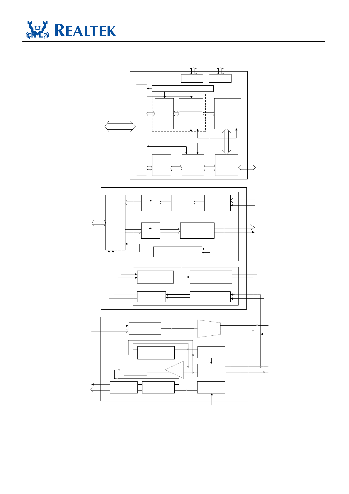
3. Block Diagram
RTL8100C & RTL8100CL
Datasheet
PCI
Interface
MII
Interface
PHY
half /full
MAC
10/100
Switch
Logic
100M
Power Control Logic
Interrupt
Control
Logic
PCI Interface + Register
FIFO
5B 4B
Decoder
4B 5B
Encoder
EEPROM
Interface
Early Interrupt
Threshold
Register
Early Interrupt
Control Logic
Control
Data
Alignment
FIFO
Logic
Scrambler
LED Driver
Packet Leng th
Transmit/
Receive
Interface
Descrambler
Register
Logic
Packet Type
Discriminator
MII
Interface
RXD
RXC 25M
TXD
TXC 25M
TXC 25M
TXD
RXC 25M
RXD
TXC10
TXD10
RXC10
RXD10
Transceiver
Serial to
Parrallel
10/100M Auto-negotiation
Control Logic
10M
Manchester Coded
Waveform
Data Recovery Receive Low Pass Filter
TD+
Variable Current
3 Level
Comparator
Slave
PLL
MLT-3
to NRZI
Parrallel
to Serial
ck
Data
Baseline
Wander
Correction
Control
Voltage
10M Output Waveform
Figure 1. Block Diagram
Shaping
3 Level
Driver
Peak
Detect
Adaptive
Equalizer
Master
PPL
25M
Link Pulse
TXO+
TXO -
RXIN+
RXIN-
Single-Chip Fast Ethernet Controller 3 Track ID: JATR-1076-21 Rev. 1.06
RTL8100C & RTL8100CL
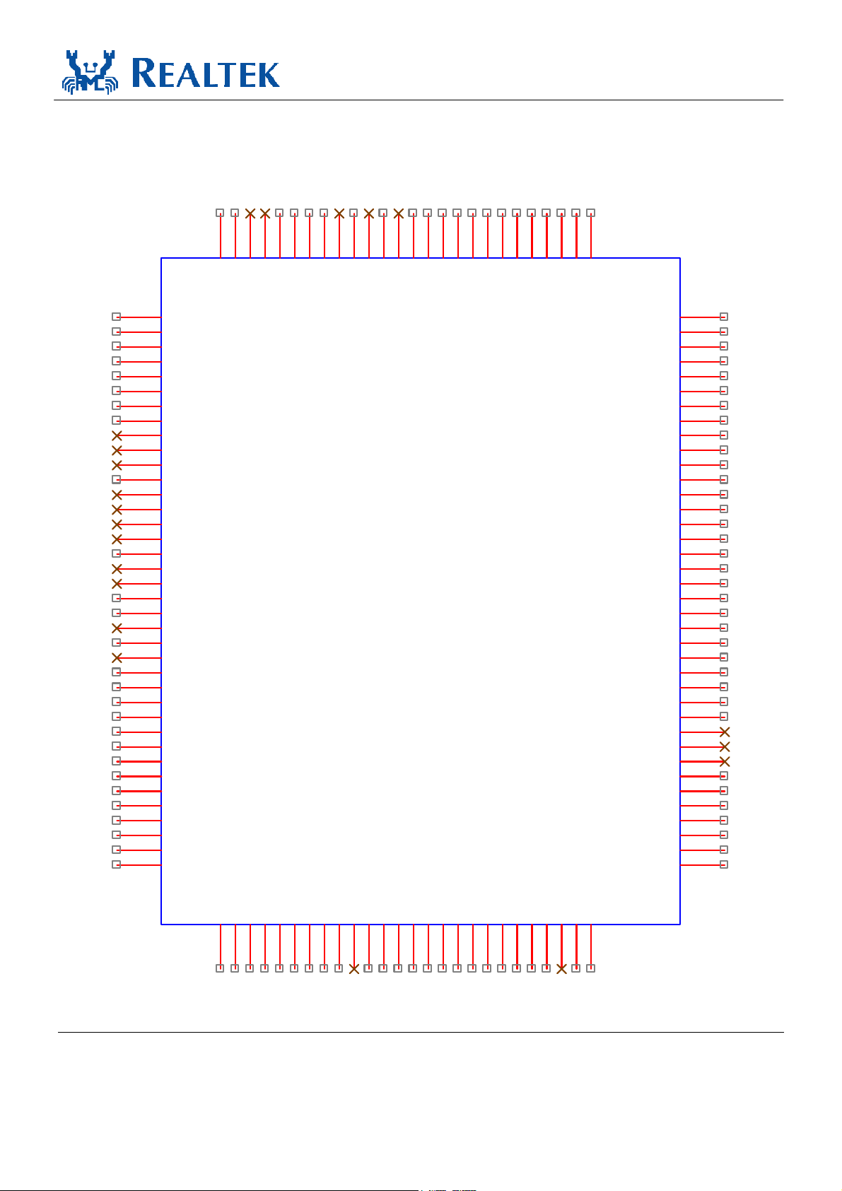
4. Pin Assignments
4.1. RTL8100C (QFP) & RTL8100CL (LQFP)
128
126
125
124
123
122
121
120
119
118
117
116
115
114
113
112
111
110
109
108
107
106
105
1
TX+
2
TX-
3
AVDD33
4
GND
5
RX+
6
RX-
7
AVDD33
8
CTRL25
9
NC
10
NC
11
NC
12
AVDD25
13
NC
14
NC
15
NC
16
NC
17
GND
18
NC
19
NC
20
AVDD33(REG)
21
GND
22
NC
23
ISOLATEB
24
NC
25
INTAB
26
VDD33
27
PCIRSTB
28
PCICLK
29
GNTB
30
REQB
31
PMEB
32
VDD25
33
AD31
34
AD30
35
GND
36
AD29
37
AD28
38
GND
127
GND
RSET
NC
NC
GND
GND
XTAL2
XTAL1
NC
NC
GND
LED0NCLED1
LED2
NC
NC
NC
EESK
EEDO
AUX / EEDI
EECS
VDD33
LANWAKE
104
103
AD0
AD1
DEVSELB
CLKRUNB
AD2
GND
GND
VDD25
AD3
AD4
AD5
AD6
VDD33
AD7
CBEB0
GND
AD8
AD9
NC
AD10
AD11
AD12
VDD33
AD13
AD14
GND
GND
AD15
VDD25
CBEB1
PAR
SERRB
NC
NC
NC
VDD33
PERRB
STOPB
TRDYB
GND
Datasheet
102
101
100
99
98
97
96
95
94
93
92
91
90
89
88
87
86
85
84
83
82
81
80
79
78
77
76
75
74
73
72
71
70
69
68
67
66
65
AD27
AD26
AD25
AD24
VDD33
39404142434445464748495051525354555657585960616263
CBEB3NCIDSEL
AD23NCAD22
AD21
GND
GND
AD20
VDD25
AD19
VDD33
AD18
AD17
AD16
CBEB2
FRAMEBNCIRDYB
NC
64
Figure 2. Pin Assignments
Single-Chip Fast Ethernet Controller 4 Track ID: JATR-1076-21 Rev. 1.06

RTL8100C & RTL8100CL
5. Pin Description
5.1. Power Management/Isolation Interface
The following signal type codes are used in the tables:
I: Input.
O: Output.
T/S: Tri-State bi-directional input/output pin.
S/T/S: Sustained Tri-State.
O/D: Open Drain.
Table 1. Power Management/Isolation Interface
Symbol Type Pin No Description
PMEB
(PME#)
ISOLATEB
(ISOLATE#)
LWAKE O 105 LAN WAKE-UP Signal.
O/D 31 Power Management Event.
Open drain, active low. Used by the RTL8100C(L) to request a
change in its current power management state and/or to indicate that
a power management event has occurred.
I 23 Isolate Pin: Active low.
Isolates the RTL8100C(L) from the PCI bus. The RTL8100C(L) does
not drive its PCI outputs (excluding PME#) and does not sample its
PCI input (including RST# and PCICLK) as long as the Isolate pin is
asserted.
Signals to the motherboard that it should execute the wake-up
process. The motherboard must support Wake-On-LAN (WOL).
There are 4 output choices, active high, active low, positive pulse,
and negative pulse, that may be asserted from the LWAKE pin. See
the LWACT bit in Table 19. CONFIG 1: Configuration Register 1,
page 23, for the setting of this output signal. The default output is an
active high signal.
When a PME event is received, LWAKE and PMEB assert at the
same time if LWPME (bit4, CONFIG4) is set to 0. If LWPME is set
to 1, LWAKE asserts only when PMEB asserts and ISOLATEB is
low.
This pin is a 3.3V signaling output pin.
Datasheet
Single-Chip Fast Ethernet Controller 5 Track ID: JATR-1076-21 Rev. 1.06

RTL8100C & RTL8100CL
5.2. PCI Interface
Table 2. PCI Interface
Symbol Type Pin No Description
AD31-0 T/S 33, 34, 36, 37, 39, 40,
42, 43, 47, 49, 50, 53,
55, 57, 58, 59, 79, 82,
83, 85, 86, 87, 89, 90,
93, 95, 96, 97, 98, 103,
104
C/BE3-0 T/S 44, 60, 77, 92 PCI Bus Command and Byte Enables Multiplexed Pins.
CLK I 28 Clock.
DEVSELB S/T/S 68 Device Select.
FRAMEB S/T/S 61 Cycle Frame.
GNTB I 29 Grant.
REQB T/S 30 Request.
IDSEL I 46 Initialization Device Select.
INTAB O/D 25 INTAB.
PCI Address and Data Multiplexed Pins.
This PCI Bus clock provides timing for all transactions and bus
phases, and is input to PCI devices. The rising edge defines the start
of each phase. The clock frequency ranges from 0 to 40MHz. For
normal network operation, the RTL8100C(L) requires a minimum
PCI clock frequency of 16.75MHz.
As a bus master, the RTL8100C (L) samples this signal to ensure that
a PCI target recognizes the destination address for the data transfer.
As a target, the RTL8100C(L) asserts this signal low when it
recognizes its target address after FRAMEB is asserted.
As a bus master, this pin indicates the beginning and duration of an
access. FRAMEB is asserted low to indicate the start of a bus
transaction. While FRAMEB is asserted, data transfer continues.
When FRAMEB is deasserted, the transaction is in the final data
phase.
As a target, the device monitors this signal before decoding the
address to check if the current transaction is addressed to it.
This signal is asserted low to indicate to the RTL8100C(L) that the
central arbiter has granted ownership of the bus to the RTL8100C(L).
This input is used when the RTL8100C(L) is acting as a bus master.
The RTL8100C(L) will assert this signal low to request the
ownership of the bus from the central arbiter.
This pin allows the RTL8100C(L) to identify when configuration
read/write transactions are intended for it.
Used to request an interrupt. It is asserted low when an interrupt
condition occurs, as defined by the Interrupt Status, Interrupt Mask
and Interrupt Enable registers.
Datasheet
Single-Chip Fast Ethernet Controller 6 Track ID: JATR-1076-21 Rev. 1.06

Symbol Type Pin No Description
IRDYB S/T/S 63 Initiator Ready.
This indicates the initiating agent’s ability to complete the current
data phase of the transaction.
As a bus master, this signal will be asserted low when the
RTL8100C(L) is ready to complete the current data phase
transaction. This signal is used in conjunction with the TRDYB
signal. Data transaction takes place at the rising edge of CLK when
both IRDYB and TRDYB are asserted low. As a target, this signal
indicates that the master has put data on the bus.
TRDYB S/T/S 67 Target Ready.
This indicates the target agent’s ability to complete the current phase
of the transaction.
As a bus master, this signal indicates that the target is ready for the
data during write operations and holds the data during read
operations. As a target, this signal will be asserted low when the
(slave) device is ready to complete the current data phase transaction.
This signal is used in conjunction with the IRDYB signal. Data
transaction takes place at the rising edge of CLK when both IRDYB
and TRDYB are asserted low.
PAR T/S 76 Parity.
This signal indicates even parity across AD31-0 and C/BE3-0
including the PAR pin. As a master, PAR is asserted during address
and write data phases. As a target, PAR is asserted during read data
phases.
PERRB S/T/S 70 Parity Error.
When the RTL8100C(L) is the bus master and a parity error is
detected, the RTL8100C(L) asserts both the SERR bit in ISR, and
Configuration Space command bit 8 (SERRB enable). Next, it
completes the current data burst transaction, then stops operation and
resets itself. After the host clears the system error, the RTL8100C(L)
continues its operation.
When the RTL8100C(L) is the bus target and a parity error is
detected, the RTL8100C(L) asserts this PERRB pin low.
SERRB O/D 75 System Error.
If an address parity error is detected and Configuration Space Status
register bit 15 (detected parity error) is enabled, the RTL8100C(L)
asserts both the SERRB pin low, and bit 14 of the Status register in
Configuration Space.
STOPB S/T/S 69 Stop.
Indicates the current target is requesting the master to stop the current
transaction.
RSTB I 27 Reset.
When RSTB is asserted low, the RTL8100C(L) performs an internal
system hardware reset. RSTB must be held for a minimum of 120ns.
RTL8100C & RTL8100CL
Datasheet
Single-Chip Fast Ethernet Controller 7 Track ID: JATR-1076-21 Rev. 1.06

RTL8100C & RTL8100CL
5.3. EPROM/EEPROM Interface/AUX
Table 3. EPROM/EEPROM Interface/AUX
Symbol Type Pin No Description
EESK
EEDO
AUX / EEDI I/O 109 Aux. Power Detect.
EECS O 106 EEPROM chip select.
O
O, I
111
108
The MA2-0 pins are switched to EESK, EEDI, EEDO in 93C46
programming or auto-load mode.
This pin is used to notify the RTL8100C(L) of the existence of Aux.
power (only during initial power-on). This pin should be pulled high
to the auxiliary power (5VPM or 3VAUX) via a resistor to detect the
Aux. power. Doing so will enable wakeup support from ACPI D3
cold or APM power-down. If this pin is not pulled high, the
RTL8100C(L) assumes that no auxiliary power exists.
EEDI: After Aux. Power On Detection is complete; EEDI is enabled
to support EEPROM auto-load operation.
Datasheet
5.4. Power Pins
Table 4. Power Pins
Symbol Type Pin No Description
VDD33 P 26, 41, 56, 71,
84, 94, 107
AVDD33 P 3, 7, 20 +3.3V (Analog).
VDD25 P 32, 54, 78, 99 +2.5V (Digital).
AVDD25 P 12 +2.5V (Analog).
GND P 4, 17, 21, 35, 38, 51,
52, 66, 80, 81, 91, 100,
101, 119, 123, 124, 128
+3.3V (Digital)
Ground.
5.5. LED Interface
Table 5. LED Interface
Symbol Type Pin No Description
LED0, 1, 2 O 117, 115, 114 LED Pins
LED0 TX/RX TX/RX TX TX
LED1 LINK100 LINK10/100 LINK10/100 LINK100
LED2 LINK10 FULL RX LINK10
During power down mode, the LEDs are OFF.
LEDS1-0 00 01 10 11
Single-Chip Fast Ethernet Controller 8 Track ID: JATR-1076-21 Rev. 1.06

RTL8100C & RTL8100CL
Datasheet
5.6. Attachment Unit Interface
Table 6. Attachment Unit Interface
Symbol Type Pin No Description
TXD+
TXDRXIN+
RXINX1 I 121 25MHz Crystal/OSC Input.
X2 O 122 Crystal Feedback Output.
O
O
1
2
I
I
5
6
100/10Base-T Transmit (TX) data.
100/10Base-T Receive (RX) data.
This output is used in a crystal connection only. It must be left open when
X1 is driven with an external 25MHz oscillator.
5.7. Test and Other Pins
Table 7. Test and Other Pins
Symbol Type Pin No Description
RTT3 TEST 123 Chip Test pin.
RTSET I/O 127 This pin must be pulled low by a resistor.
Refer to section 9 Application Information, page 61, for the correct
value.
CTRL25 Analog 8 Use this pin and an external PNP type transistor to generate +2.5V for
the RTL8100C(L).
CLKRUN I/O 65 Clock Run.
This signal is used to request starting (or speeding up) of the clock.
CLKRUN also indicates the clock status. CLKRUN is an open drain
output as well as an input. The RTL8100C(L) requests the central
resource to start, speed up, or maintain the interface clock by the
assertion of CLKRUN. For the host system, it is an S/T/S signal. The
host system (central resource) is responsible for maintaining
CLKRUN asserted, and for driving it high to the negated (deasserted)
state.
NC - 9~11,13~16, 18, 19, 22,
24, 45, 48, 62, 72~74,
110, 112, 116, 118,
120, 125, 126
Not Connected.
Single-Chip Fast Ethernet Controller 9 Track ID: JATR-1076-21 Rev. 1.06

RTL8100C & RTL8100CL
Datasheet
5.8. Register Descriptions
The RTL8100C(L) provides the following set of operational registers mapped into PCI memory space or
I/O space.
Table 8. Register Descriptions
Offset R/W Tag Description
0000h R/W IDR0 ID Register 0.
ID registers 0-5 are only permitted to read/write via 4-byte access.
Read access can be byte, word, or double word access. The initial
value is autoloaded from the EEPROM EthernetID field.
0001h R/W IDR1 ID Register 1.
0002h R/W IDR2 ID Register 2.
0003h R/W IDR3 ID Register 3.
0004h R/W IDR4 ID Register 4.
0005h R/W IDR5 ID Register 5.
0006h-0007h - - Reserved.
0008h R/W MAR0 Multicast Address Register 0.
The MAR register 0-7 are only permitted to read/write via 4-byte
access. Read access can be byte, word, or double word access. The
driver is responsible for initializing these registers.
0009h R/W MAR1 Multicast Address Register 1.
000Ah R/W MAR2 Multicast Address Register 2.
000Bh R/W MAR3 Multicast Address Register 3.
000Ch R/W MAR4 Multicast Address Register 4.
000Dh R/W MAR5 Multicast Address Register 5.
000Eh R/W MAR6 Multicast Address Register 6.
000Fh R/W MAR7 Multicast Address Register 7.
0010h-0013h R/W TSD0 Transmit Status of Descriptor 0.
0014h-0017h R/W TSD1 Transmit Status of Descriptor 1.
0018h-001Bh R/W TSD2 Transmit Status of Descriptor 2.
001Ch-001Fh R/W TSD3 Transmit Status of Descriptor 3.
0020h-0023h R/W TSAD0 Transmit Start Address of Descriptor 0.
0024h-0027h R/W TSAD1 Transmit Start Address of Descriptor 1.
0028h-002Bh R/W TSAD2 Transmit Start Address of Descriptor 2.
002Ch-002Fh R/W TSAD3 Transmit Start Address of Descriptor 3.
0030h-0033h R/W RBSTART Receive (Rx) Buffer Start Address.
0034h-0035h R ERBCR Early Receive (Rx) Byte Count Register.
0036h R ERSR Early Rx Status Register.
0037h R/W CR Command Register.
0038h-0039h R/W CAPR Current Address of Packet Read.
003Ah-003Bh R CBR Current Buffer Address.
The initial value is 0000h. It reflects total received byte-count in the
Rx buffer.
003Ch-003Dh R/W IMR Interrupt Mask Register.
003Eh-003Fh R/W ISR Interrupt Status Register.
0040h-0043h R/W TCR Transmit (Tx) Configuration Register.
Single-Chip Fast Ethernet Controller 10 Track ID: JATR-1076-21 Rev. 1.06

RTL8100C & RTL8100CL
Datasheet
Offset R/W Tag Description
0044h-0047h R/W RCR Receive (Rx) Configuration Register.
0048h-004Bh R/W TCTR Timer CounT Register.
This register contains a 32-bit general-purpose timer. Writing any
value to this register will reset the original timer and start a count
from zero.
004Ch-004Fh R/W MPC Missed Packet Counter.
Indicates the number of packets discarded due to Rx FIFO
overflow. It is a 24-bit counter. After s/w reset, MPC is cleared.
Only the lower 3 bytes are valid.
When any value is written, MPC will be reset also.
0050h R/W 9346CR 93C46 Command Register.
0051h R/W CONFIG0 Configuration Register 0.
0052h R/W CONFIG1 Configuration Register 1.
0053H - - Reserved.
0054h-0057h R /W TimerInt Timer Interrupt Register.
Once having written a non-zero value to this register, the Timeout
bit of the ISR register will be set whenever the TCTR reaches that
value. The Timeout bit will never be set whilst the TimerInt register
is zero.
0058h R/W MSR Media Status Register.
0059h R/W CONFIG3 Configuration register 3.
005Ah R/W CONFIG4 Configuration register 4.
005Bh - - Reserved.
005Ch-005Dh R/W MULINT Multiple Interrupt Select.
005Eh R RERID PCI Revision ID = 10h.
005Fh - - Reserved.
0060h-0061h R TSAD Transmit Status of All Descriptors.
0062h-0063h R/W BMCR Basic Mode Control Register.
0064h-0065h R BMSR Basic Mode Status Register.
0066h-0067h R/W ANAR Auto-Negotiation Advertisement Register.
0068h-0069h R ANLPAR Auto-Negotiation Link Partner Register.
006Ah-006Bh R ANER Auto-Negotiation Expansion Register.
006Ch-006Dh R DIS Disconnect Counter.
006Eh-006Fh R FCSC False Carrier Sense Counter.
0070h-0071h R/W NWAYTR N-way Test Register.
0072h-0073h R REC RX_ER Counter.
0074h-0075h R/W CSCR CS Configuration Register.
0076-0077h - - Reserved.
0078h-007Bh R/W PHY1_PARM PHY Parameter 1.
007Ch-007Fh R/W TW_PARM Twister Parameter.
0080h R/W PHY2_PARM PHY Parameter 2.
0081-0083h - - Reserved.
0084h R/W CRC0 Power Management CRC register 0 for wakeup frame 0.
0085h R/W CRC1 Power Management CRC register 1 for wakeup frame 1.
0086h R/W CRC2 Power Management CRC register 2 for wakeup frame 2.
0087h R/W CRC3 Power Management CRC register 3 for wakeup frame 3.
0088h R/W CRC4 Power Management CRC register 4 for wakeup frame 4.
Single-Chip Fast Ethernet Controller 11 Track ID: JATR-1076-21 Rev. 1.06

RTL8100C & RTL8100CL
Datasheet
Offset R/W Tag Description
0089h R/W CRC5 Power Management CRC register 5 for wakeup frame 5.
008Ah R/W CRC6 Power Management CRC register 6 for wakeup frame 6.
008Bh R/W CRC7 Power Management CRC register 7 for wakeup frame 7.
008Ch–0093h R/W Wakeup0 Power Management Wakeup frame 0 (64-bit).
0094h–009Bh R/W Wakeup1 Power Management Wakeup frame 1 (64-bit).
009Ch–00A3h R/W Wakeup2 Power Management Wakeup frame 2 (64-bit).
00A4h–00ABh R/W Wakeup3 Power Management Wakeup frame 3 (64-bit).
00ACh–00B3h R/W Wakeup4 Power Management Wakeup frame 4 (64-bit).
00B4h–00BBh R/W Wakeup5 Power Management Wakeup frame 5 (64-bit).
00BCh–00C3h R/W Wakeup6 Power Management Wakeup frame 6 (64-bit).
00C4h–00CBh R/W Wakeup7 Power Management Wakeup frame 7 (64-bit).
00CCh R/W LSBCRC0 LSB of the mask byte of wakeup frame 0 within offset 12 to 75.
00CDh R/W LSBCRC1 LSB of the mask byte of wakeup frame 1 within offset 12 to 75.
00CEh R/W LSBCRC2 LSB of the mask byte of wakeup frame 2 within offset 12 to 75.
00CFh R/W LSBCRC3 LSB of the mask byte of wakeup frame 3 within offset 12 to 75.
00D0h R/W LSBCRC4 LSB of the mask byte of wakeup frame 4 within offset 12 to 75.
00D1h R/W LSBCRC5 LSB of the mask byte of wakeup frame 5 within offset 12 to 75.
00D2h R/W LSBCRC6 LSB of the mask byte of wakeup frame 6 within offset 12 to 75.
00D3h R/W LSBCRC7 LSB of the mask byte of wakeup frame 7 within offset 12 to 75.
00D4h-00D7h - - Reserved.
00D8h R/W Config5 Configuration register 5.
00D9h-00FFh - - Reserved.
5.9. Receive Status Register in RX Packet Header
Table 9. Receive Status Register in RX Packet Header
Bit R/W Symbol Description
15 R MAR Multicast Address Received.
This bit set to 1 indicates that a multicast packet has been received.
14 R PAM Physical Address Matched.
This bit set to 1 indicates that the destination address of this packet
matches the value written in ID registers.
13 R BAR Broadcast Address Received.
This bit set to 1 indicates that a broadcast packet is received. BAR,
MAR bit will not be set simultaneously.
12-6 - - Reserved.
5 R ISE Invalid Symbol Error (100Base-TX only).
This bit set to 1 indicates that an invalid symbol was encountered during
the reception of this packet.
4 R RUNT Runt Packet Received.
This bit set to 1 indicates that the received packet length is smaller than
64 bytes ( i.e. media header + data + CRC < 64 bytes )
3 R LONG Long Packet.
This bit set to 1 indicates that the size of the received packet exceeds
4k bytes.
Single-Chip Fast Ethernet Controller 12 Track ID: JATR-1076-21 Rev. 1.06

RTL8100C & RTL8100CL
Datasheet
Bit R/W Symbol Description
2 R CRC Cyclic Redundancy Check (CRC) Error.
When set, indicates that a CRC error occurred on the received
packet.
1 R FAE Frame Alignment Error.
When set, indicates that a frame alignment error occurred on this
received packet.
0 R ROK Receive OK.
When set, indicates that a good packet was received.
5.10. Transmit Status Register
(TSD0-3)(Offset 0010h-001Fh, R/W)
The read-only bits (CRS, TABT, OWC, CDH, NCC3-0, TOK, TUN) will be cleared by the RTL8100C(L)
when the Transmit Byte Count (bits 12-0) in the corresponding Tx descriptor is written. It is not affected
when software writes to these bits. These registers are only permitted to be written via double-word access.
After a software reset, all bits except OWN bit are reset to 0.
Table 10. Transmit Status Register
Bit R/W Symbol Description
31 R CRS Carrier Sense Lost.
This bit is set to 1 when the carrier is lost during transmission of a
packet.
30 R TABT Transmit Abort.
This bit is set to 1 if the transmission of a packet was aborted. This bit
is read only, writing to this bit is not affected.
29 R OWC Out of Window Collision.
This bit is set to 1 if the RTL8100C(L) encountered an ‘out of window’
collision during the transmission of a packet.
28 R CDH CD HeartBeat.
The NIC watches for a collision signal (i.e., CD Heartbeat signal)
during the first 6.4µs of the InterFrame Gap following a
transmission. This bit is set if the transceiver fails to send this signal.
This bit is cleared in 100Mbps mode.
27-24 R NCC3-0 Number of Collision Count.
Indicates the number of collisions encountered during the
transmission of a packet.
23-22 - - Reserved.
21-16 R/W ERTXTH5-0 Early Tx Threshold.
Specifies the threshold level in the Tx FIFO to begin the
transmission. When the byte count of the data in the Tx FIFO reaches
this level, (or the FIFO contains at least one complete packet) the
RTL8100C(L) will transmit this packet.
000000 = 8 bytes
These fields count from 000001 to 111111 in units of 32 bytes.
This threshold must be prevented from exceeding 2k bytes.
Single-Chip Fast Ethernet Controller 13 Track ID: JATR-1076-21 Rev. 1.06

RTL8100C & RTL8100CL
Datasheet
Bit R/W Symbol Description
15 R TOK Transmit OK.
Set to 1 indicates that the transmission of a packet was completed
successfully and no transmit underrun has occurred.
14 R TUN Transmit FIFO Underrun.
Set to 1 if the Tx FIFO was exhausted during the transmission of a
packet. The RTL8100C(L) can re-transfer data if the Tx FIFO
underruns. That is, when TSD<TUN>=1, TSD<TOK>=0 and
ISR<TOK>=1 (or ISR<TER>=1).
13 R/W OWN OWN.
The RTL8100C(L) sets this bit to 1 when the Tx DMA operation of
this descriptor has completed. The driver must set this bit to 0 when
the Transmit Byte Count (bits 0-12) is written. The default value is 1.
12-0 R/W SIZE Descriptor Size.
The total size in bytes of the data in this descriptor. If the packet
length is more than 1792 bytes (0700h), the Tx queue will be invalid,
i.e. the next descriptor will be written only after the OWN bit of that
long packet’s descriptor has been set.
5.11. ERSR: Early RX Status Register (Offset 0036h, R)
Table 11. ERSR: Early RX Status Register
Bit R/W Symbol Description
7-4 - - Reserved.
3 R ERGood Early Rx Good packet.
This bit is set whenever a packet is completely received and the
packet is good. Writing a 1 to this bit will clear it.
2 R ERBad Early Rx Bad packet.
This bit is set whenever a packet is completely received and the
packet is bad. Writing a 1 to this bit will clear it.
1 R EROVW Early Rx OverWrite.
This bit is set when the RTL8100C(L)’s local address pointer is equal
to CAPR. In Early Mode, this is different from buffer overflow. It
happens when the RTL8100C(L) detects an Rx error and wants to fill
another packet data from the beginning address of that error packet.
Writing a 1 to this bit will clear it.
0 R EROK Early Rx OK.
The power-on value is 0. It is set when the Rx byte count of the
arriving packet exceeds the Rx threshold. After the whole packet is
received, the RTL8100C(L) will set ROK or RER in ISR and clear
this bit simultaneously. Setting this bit will invoke an ROK interrupt.
Single-Chip Fast Ethernet Controller 14 Track ID: JATR-1076-21 Rev. 1.06

RTL8100C & RTL8100CL
Datasheet
5.12. Command Register (Offset 0037h, R/W)
This register is used for issuing commands to the RTL8100C(L). These commands are issued by setting the
corresponding bits for the function. A global software reset along with individual reset and enable/disable for
transmitter and receiver are provided here.
Table 12. Command Register
Bit R/W Symbol Description
7-5 - - Reserved.
4 R/W RST Reset.
Setting to 1 forces the RTL8100C(L) to a software reset state which
disables the transmitter and receiver, reinitializes the FIFOs, resets
the system buffer pointer to the initial value (Tx buffer is at TSAD0,
Rx buffer is empty). The values of IDR0-5 and MAR0-7 and PCI
configuration space will have no changes. This bit is 1 during the
reset operation, and is cleared to 0 by the RTL8100C(L) when the
reset operation is complete.
3 R/W RE Receiver Enable.
When set to 1, makes the idle receive state machine active. This bit
will read back as a 1 whenever the receive state machine is active.
After initial power-up, software must ensure that the receiver has
completely reset before setting this bit. This bit will be reset after PCI
reset deassertion.
2 R/W TE Transmitter Enable.
When set to 1, and the transmit state machine is idle, then the transmit
state machine becomes active. This bit will read back as a 1 whenever
the transmit state machine is active. After initial power-up, software
must ensure that the transmitter has completely reset before setting
this bit. This bit will be reset after PCI reset deassertion.
1 - - Reserved.
0 R BUFE Buffer Empty.
RX Buffer Empty. There are no packets stored in the RX buffer ring.
5.13. Interrupt Mask Register (Offset 003Ch-003Dh, R/W)
This register masks the interrupts that can be generated from the Interrupt Status Register. A hardware reset
will clear all mask bits. Setting a mask bit allows the corresponding bit in the Interrupt Status Register to
cause an interrupt. The Interrupt Status Register bits are always set to 1 if the condition is present,
regardless of the state of the corresponding mask bit.
Table 13. Interrupt Mask Register
Bit R/W Symbol Description
15 R/W SERR System Error Interrupt.
1: Enable
0: Disable
14 R/W TimeOut Time Out Interrupt.
1: Enable
0: Disable
Single-Chip Fast Ethernet Controller 15 Track ID: JATR-1076-21 Rev. 1.06

RTL8100C & RTL8100CL
Bit R/W Symbol Description
13 R/W LenChg Cable Length Change Interrupt.
1: Enable
0: Disable
12-7 - - Reserved.
6 R/W FOVW Rx FIFO Overflow Interrupt.
1: Enable
0: Disable
5 R/W PUN/LinkChg Packet Underrun/Link Change Interrupt.
1: Enable
0: Disable
4 R/W RXOVW Rx Buffer Overflow Interrupt.
1: Enable
0: Disable
3 R/W TER Transmit Error Interrupt.
1: Enable
0: Disable
2 R/W TOK Transmit OK Interrupt.
1: Enable
0: Disable
1 R/W RER Receive Error Interrupt.
1: Enable
0: Disable
0 R/W ROK Receive OK Interrupt.
1: Enable
0: Disable
Datasheet
5.14. Interrupt Status Register (Offset 003Eh-003Fh, R/W)
This register indicates the source of an interrupt when the INTA pin goes active. Enabling the
corresponding bits in the Interrupt Mask Register (IMR) allows bits in this register to produce an interrupt.
When an interrupt is active, one or more bits in this register are set to 1. The interrupt Status Register
reflects all current pending interrupts, regardless of the state of the corresponding mask bit in the IMR.
Reading the ISR clears all interrupts. Writing to the ISR has no effect.
Table 14. Interrupt Status Register
Bit R/W Symbol Description
15 R/W SERR System Error.
Set to 1 when the RTL8100C(L) signals a system error on the PCI
bus.
14 R/W TimeOut Time Out.
Set to 1 when the TCTR register reaches the value of the TimerInt
register.
13 R/W LenChg Cable Length Change.
Cable length is changed after Receiver is enabled.
12 - 7 - - Reserved.
Single-Chip Fast Ethernet Controller 16 Track ID: JATR-1076-21 Rev. 1.06

RTL8100C & RTL8100CL
Bit R/W Symbol Description
6 R/W FOVW Rx FIFO Overflow.
Set when an overflow occurs on the Rx status FIFO.
5 R/W PUN/LinkChg Packet Underrun/Link Change.
Set to 1 when CAPR is written but Rx buffer is empty, or when link
status is changed.
4 R/W RXOVW Rx Buffer Overflow.
Set when receive (Rx) buffer ring storage resources have been
exhausted.
3 R/W TER Transmit (Tx) Error.
Indicates that a packet transmission was aborted, due to excessive
collisions, according to the TXRR’s setting.
2 R/W TOK Transmit (Tx) OK.
Indicates that a packet transmission has completed successfully.
1 R/W RER Receive (Rx) Error.
Indicates that a packet has either a CRC error or Frame Alignment
Error (FAE). Collided frames will not be recognized as CRC errors if
the length of the frame is shorter than 16 bytes.
0 R/W ROK Receive (Rx) OK.
In normal mode, indicates the successful completion of a packet
reception. In early mode, indicates that the Rx byte count of the
arriving packet exceeds the early Rx threshold.
Datasheet
5.15. Transmit Configuration Register (Offset 0040h-0043h, R/W)
This register defines the Transmit Configuration for the RTL8100C(L). It controls such functions as
Loopback, programmable InterFrame Gap, Fill and Drain Thresholds, and maximum DMA burst size.
Table 15. Transmit Configuration Register
Bit R/W Symbol Description
31 - - Reserved.
30~26 R HWVERID_A
Hardware Version ID A.
RTL8139 1 1 0 0 0 0 0
RTL8139A 1 1 1 0 0 0 0
RTL8139A-G 1 1 1 0 1 0 0
RTL8139B 1 1 1 1 0 0 0
RTL8130 1 1 1 1 0 0 0
RTL8139C 1 1 1 0 1 0 0
RTL8100 1 1 1 1 0 1 0
RTL8100B
RTL8100C
RTL8139D
RTL8139C+ 1 1 1 0 1 1 0
RTL8101 1 1 1 0 1 1 1
Reserved Other combinations.
Bit30 Bit29 Bit28 Bit27 Bit26 Bit23 Bit2
2
1 1 1 0 1 0 1
Single-Chip Fast Ethernet Controller 17 Track ID: JATR-1076-21 Rev. 1.06

RTL8100C & RTL8100CL
Bit R/W Symbol Description
25, 24 R/W IFG1, 0 InterFrame Gap time.
This field allows the user to adjust the InterFrame Gap time below the
standard: 9.6µs for 10Mbps, 960ns for 100Mbps. The time can be
programmed from 9.6µs to 8.4µs (10Mbps) and 960ns to 840ns
(100Mbps). Note that any value other than (1, 1) will violate the
IEEE 802.3 standard.
The formula for the InterFrame Gap is:
10 Mbps: 8.4µs + 0.4(IFG(1:0)) µs
100 Mbps: 840ns + 40(IFG(1:0)) ns
23, 22 R HWVERID_B Hardware Version ID B.
21~19 - - Reserved.
18, 17 R/W LBK1, LBK0 Loopback test.
There will be no packets on the TX+/- lines under the Loopback test
condition. The loopback function must be independent of the link
state.
00: Normal operation
01: Reserved
10: Reserved
11: Loopback mode
16 R/W CRC Append CRC.
Setting to 1 means that there is no CRC appended at the end of a
packet. Setting to 0 means that there is a CRC appended at the end of
a packet.
15~11 - - Reserved.
10~8 R/W MXDMA2, 1, 0 Max DMA Burst Size per Tx DMA Burst.
This field sets the maximum size of transmit DMA data bursts
according to the following table:
000 = 16 bytes
001 = 32 bytes
010 = 64 bytes
011 = 128 bytes
100 = 256 bytes
101 = 512 bytes
110 = 1024 bytes
111 = 2048 bytes
7-4 R/W TXRR Tx Retry Count.
These are used to specify additional transmission retries in multiple
of 16 (IEEE 802.3 CSMA/CD retry count). If the TXRR is set to 0,
the transmitter will re-transmit 16 times before aborting due to
excessive collisions. If the TXRR is set to a value greater than 0, the
transmitter will re-transmit a number of times equals to the following
formula before aborting:
Total retries = 16 + (TXRR * 16)
The TER bit in the ISR register or transmit descriptor will be set
when the transmission fails and reaches to this specified retry count.
3-1 - - Reserved.
0 W CLRABT Clear Abort.
Setting this bit to 1 causes the RTL8100C(L) to retransmit the packet
at the last transmitted descriptor when this transmission was aborted,
Setting this bit is only permitted in the transmit abort state.
Datasheet
Single-Chip Fast Ethernet Controller 18 Track ID: JATR-1076-21 Rev. 1.06

RTL8100C & RTL8100CL
Datasheet
5.16. Receive Configuration Register
(Offset 0044h-0047h, R/W)
This register is used to set the receive configuration for the RTL8100C(L). Receive properties such as
accepting error packets, runt packets, setting the receive drain threshold etc. are controlled here.
Table 16. Receive Configuration Register
Bit R/W Symbol Description
31-28 - - Reserved.
27-24 R/W ERTH3, 2, 1, 0 Early Rx threshold bits.
These bits are used to select the Rx threshold multiplier of a whole
packet that has been transferred to the system buffer in early mode
whilst the frame protocol is under the RTL8100C(L)'s definition.
0000 = No early Rx threshold 0001 = 1/16
0010 = 2/16 0011 = 3/16
0100 = 4/16 0101 = 5/16
0110 = 6/16 0111 = 7/16
1000 = 8/16 1001 = 9/16
1010 = 10/16 1011 = 11/16
1100 = 12/16 1101 = 13/16
1110 = 14/16 1111 = 15/16
23-18 - - Reserved.
17 R/W MulERINT Multiple Early Interrupt select.
When this bit is set, any received packet invokes early interrupt
according to MULINT<MISR[11:0]> setting in early mode. When
this bit is reset, the packets of familiar protocols (IPX, IP, NDIS, etc)
invoke early interrupt according to RCR<ERTH[3:0]> setting in
early mode. The packets of unfamiliar protocols will invoke early
interrupt according to the setting of MULINT<MISR[11:0]>.
16 R/W RER8 Receive Error 8 bytes.
1: The RTL8100C(L) accepts error packets with a length of 8~64
bytes.
0: The RTL8100C(L) accepts error packets with a length larger than
64 bytes. The power-on default is zero.
If AER or AR is set, the RER (Receive Error) will be set when the
RTL8100C(L) receives an error packet with a length larger than
8 bytes. RER8 is irrelevant in this situation.
Single-Chip Fast Ethernet Controller 19 Track ID: JATR-1076-21 Rev. 1.06

RTL8100C & RTL8100CL
Bit R/W Symbol Description
15~13 R/W RXFTH2, 1, 0 Rx FIFO Threshold.
Specifies the Rx FIFO Threshold level. When the number of received
data bytes from a packet that is being received into the RTL8100C(L)’s
Rx FIFO has reached this level (or the FIFO contains a complete
packet), the receive PCI bus master function will begin to transfer the
data from the FIFO to the host memory. This field sets the threshold
level according to the following table:
000 = 16 bytes
001 = 32 bytes
010 = 64 bytes
011 = 128 bytes
100 = 256 bytes
101 = 512 bytes
110 = 1024 bytes
111 = No Rx threshold. The RTL8100C(L) begins the transfer of data
after receiving a whole packet in the FIFO.
12, 11 R/W RBLEN1, 0 Rx Buffer Length.
This field indicates the size of the Rx ring buffer:
00 = 8k + 16 bytes
01 = 16k + 16 bytes
10 = 32K + 16 bytes
11 = 64K + 16 bytes
10~8 R/W MXDMA2, 1, 0 Max DMA Burst Size per Rx DMA Burst.
This field sets the maximum size of the receive DMA data bursts:
000 = 16 bytes
001 = 32 bytes
010 = 64 bytes
011 = 128 bytes
100 = 256 bytes
101 = 512 bytes
110 = 1024 bytes
111 = Unlimited
7 R/W W RAP Wraps packet data into the beginning of the Rx buffer.
0: The RTL8100C(L) will transfer the rest of the packet data into the
beginning of the Rx buffer if this packet has not been completely moved into
the Rx buffer and the transfer has arrived at the end of the Rx buffer.
1: The RTL8100C(L) will keep moving the rest of the packet data into
the memory immediately after the end of the Rx buffer, if this packet has
not been completely moved into the Rx buffer and the transfer has
arrived at the end of the Rx buffer. The software driver must reserve at
least 1.5 Kbytes buffer to accept the remainder of the packet. We assume
that the remainder of the packet is X bytes. The next packet will be
moved into the memory from the X byte offset at the top of the Rx
buffer.
This bit is invalid when the Rx buffer is set to 64 Kbytes.
6 - - Reserved.
Datasheet
Single-Chip Fast Ethernet Controller 20 Track ID: JATR-1076-21 Rev. 1.06

RTL8100C & RTL8100CL
Bit R/W Symbol Description
5 R/W AER Accept Error Packet.
1: Packets with CRC errors, alignment errors, and/or collided fragments
will be accepted.
0: Packets with the above errors will be rejected.
4 R/W AR Accept Runt.
This bit allows the receiver to accept packets that are smaller than
64 bytes. The packet must be at least 8 bytes long to be accepted as a
runt.
1: Accept
0: Reject
3 R/W AB Accept Broadcast packets.
1: Accept
0: Reject
2 R/W AM Accept Multicast packets.
1: Accept
0: Reject
1 R/W APM Accept Physical Match packets.
1: Accept
0: Reject
0 R/W AAP Accept All Packets.
Set to 1 to accept all packets with a physical destination address.
1: Accept
0: Reject
Datasheet
Single-Chip Fast Ethernet Controller 21 Track ID: JATR-1076-21 Rev. 1.06

RTL8100C & RTL8100CL
Datasheet
5.17. 9346CR: 93C46 Command Register
(Offset 0050h, R/W)
This register is used for issuing commands to the RTL8100C(L). These commands are issued by setting the
corresponding bits for the function. A warm software reset along with individual reset and enable/disable for
transmitter and receiver are also provided.
Table 17. 9346CR: 93C46 Command Register
Bit R/W Symbol Description
7-6 R/W EEM1-0 Operating Mode: These 2 bits set the RTL8100C(L) operating mode.
0 0 Normal: RTL8100C(L) network/host
0 1 Auto-load: Entering this mode will force the
1 0 93C46 Programming: In this mode, both
1 1 Config Register Write Enable: Before writing
4-5 - - Reserved.
3 R/W EECS
2 R/W EESK
1 R/W EEDI
0 R EEDO
EEM1 EEM0 Operating Mode
communication mode.
RTL8100C(L) to load the contents of the
93C46 as if an RSTB signal had been asserted.
This auto-load operation will take about 2ms.
After it is completed, the RTL8100C(L) goes
back to normal mode automatically
(EEM1 = 0 EEM0 = 0) and all other
registers are reset to default values.
network and host bus master operations are
disabled. The 93C46 can be directly accessed
via bit3-0 which now reflects the states of
EECS, EESK, EEDI, & EEDO pins
respectively.
to CONFIG0, 1, 3, 4 registers, and bit 13, 12,
and 8 of BMCR (offset 62h-63h), the
RTL8100C(L) must be placed in this mode.
This will protect the RTL8100C(L)’s
configuration from accidental change.
These bits reflect the state of EECS, EESK, EEDI, and EEDO pins in
auto-load or 93C46 programming mode.
Single-Chip Fast Ethernet Controller 22 Track ID: JATR-1076-21 Rev. 1.06

RTL8100C & RTL8100CL
5.18. CONFIG 0: Configuration Register 0
(Offset 0051h, R/W)
Table 18. CONFIG 0: Configuration Register 0
Bit R/W Symbol Description
7 R SCR Scrambler Mode.
Always 0.
6 R PCS PCS Mode.
Always 0.
5 R T10 10Mbps Mode.
Always 0.
4-3 R PL1, PL0 10Mbps Medium Type.
Always (PL1, PL0) = (1, 0).
2-0 - - Reserved.
5.19. CONFIG 1: Configuration Register 1
Datasheet
(Offset 0052h, R/W)
Table 19. CONFIG 1: Configuration Register 1
Bit R/W Symbol Description
7-6 R/W LEDS1-0 Refer to section 5.5 LED Interface, page 8, for a detailed LED pin description. The
initial value of these bits comes from the 93C46.
5 R/W DVRLOAD Driver Load.
Software may use this bit to make sure that the driver has been loaded.
1: Driver loaded
0: Driver not loaded
When the command register bits IOEN, MEMEN, and BMEN of the PCI
configuration space are written, the RTL8100C(L) will clear this bit
automatically.
4 R/W LWACT
3 R MEMMAP Memory Mapping.
2 R IOMAP I/O Mapping.
LWAKE active mode: The LWACT bit and LWPTN bit in CONFIG4 register
are used to program the LWAKE pin’s output signal. Depending on the
combination of these two bits, there may be 4 choices of LWAKE signal, i.e.,
active high, active low, positive (high) pulse, and negative (low) pulse. The
output pulse width is about 150ms.
The default value of each of these two bits is 0, i.e., the default output signal of
the LWAKE pin is an active high signal.
LW PT N
* Default value.
Operational registers are mapped into PCI memory space.
Operational registers are mapped into PCI I/O space.
0
1 Positive pulse Negative pulse
Active high* Active low
LWACT LWAKE Output
0 1
Single-Chip Fast Ethernet Controller 23 Track ID: JATR-1076-21 Rev. 1.06

Bit R/W Symbol Description
1 R/W VPD Set to enable Vital Product Data.
VPD data is stored in the 93C46 from within offset 40h-7Fh.
0 R/W PMEn Power Management Enable.
Writable only when the 93C46CR register EEM1:0 = [1:1].
Let A denote the New_Cap bit (bit 4 of the Status Register) in the PCI
Configuration space offset 06H.
Let B denote the Cap_Ptr register in the PCI Configuration space offset 34H.
Let C denote the Cap_ID (power management) register in the PCI
Configuration space offset 50H.
Let D denote the power management registers in the PCI Configuration space
offset from 52H to 57H.
Let E denote the Next_Ptr (power management) register in the PCI
Configuration space offset 51H.
PMEn Description
1: A=1, B=50h, C=01h, D valid, E=0
0: A=B=C=E=0, D not valid
RTL8100C & RTL8100CL
Datasheet
5.20. Media Status Register (Offset 0058h, R/W)
This register allows configuration of device and PHY options, and provides PHY status information.
Table 20. Media Status Register
Bit R/W Symbol Description
7 R/W TXFCE/
LdTXFCE
6 R/W RXFCE RX Flow control Enable.
5 - - Reserved.
4 R Aux_Status Aux. Power present Status.
Tx Flow Control Enable.
Flow control is valid in full-duplex mode only. This register’s default
value comes from the 93C46.
RTL8100C(L) Remote TXFCE/LdTXFCE
ANE = 1 NWAY FLY mode R/O
ANE = 1 NWAY mode only R/W
ANE = 1 No NWAY R/W
ANE = 0 &
full-duplex mode
ANE = 0 &
half-duplex mode
NWAY FLY mode: NWAY with flow control capability.
NWAY mode only: NWAY without flow control capability.
Flow control is enabled in full-duplex mode only. The default value
comes from the 93C46.
1: Aux. Power is present
0: Aux. Power is absent
The value of this bit is fixed after each PCI reset.
- R/W
- Invalid
Single-Chip Fast Ethernet Controller 24 Track ID: JATR-1076-21 Rev. 1.06

RTL8100C & RTL8100CL
Bit R/W Symbol Description
3 R SPEED_10 Speed. Set when current media is 10Mbps. Reset, when current media
is 100Mbps.
2 R LINKB Inverse of Link status.
0: Link OK
1: Link Fail.
1 R TXPF Transmit Pause Flag.
Set when the RTL8100C(L) sends a pause packet. Reset when the
RTL8100C(L) sends a timer done packet.
0 R RXPF Receive Pause Flag.
Set when the RTL8100C(L) is in backoff state because a pause packet
was received.
Reset when the pause state is cleared.
5.21. CONFIG 3: Configuration Register3
(Offset 0059h, R/W)
Table 21. CONFIG 3: Configuration Register3
Bit R/W Symbol Description
7 R GNTSel Grant Select.
Sets the Frame’s asserted time after the Grant signal has been
asserted. Frame and Grant are PCI signals.
1: Delay one clock from GNT assertion
0: No delay
6 R/W PARM_En Parameter Enable (Used in 100Mbps mode only).
0: The 9346CR register EEM1:0 = [1:1] will enable the
PHY1_PARM, PHY2_PARM, and TW_PARM registers to be written
via software.
1: Allows parameters to be auto-loaded from the 93C46, and disables
writing to PHY1_PARM, PHY2_PARM and TW_PARM registers
via software. PHY1_PARM and PHY2_PARM can be auto-loaded
from the EEPROM in this mode. The parameter auto-load process is
executed each time the Link is OK in 100Mbps mode.
Datasheet
Single-Chip Fast Ethernet Controller 25 Track ID: JATR-1076-21 Rev. 1.06

RTL8100C & RTL8100CL
Bit R/W Symbol Description
5 R/W Magic Magic Packet.
This bit is valid when the PWEn bit of the CONFIG1 register is set.
The RTL8100C(L) will assert the PMEB signal to wakeup the
operating system when a Magic Packet is received.
Once the RTL8100C(L) has been enabled for Magic Packet wakeup,
it scans all incoming packets addressed to the node for a specific data
sequence that indicates to the controller that this is a Magic Packet. A
Magic Packet must also meet the basic requirements of:
Destination address + Source address + data + CRC.
The destination address may be the node ID of the receiving station or
a multicast address, which includes the broadcast address.
The specific sequence consists of 16 duplications of a 6-byte ID
register, with no breaks nor interrupts. This sequence can be located
anywhere within the packet, but must be preceded by a
synchronization stream, 6 bytes of FFh. The device will also accept a
multicast address, as long as the 16 duplications of the IEEE MAC
address match the address of the ID register.
If the Node ID is 11h 22h 33h 44h 55h 66h, then the magic packet’s
format is similar to the following:
Destination address + source address + MISC + FF FF FF FF FF FF +
MISC + 11 22 33 44 55 66 + 11 22 33 44 55 66 + 11 22 33 44 55 66 +
11 22 33 44 55 66 + 11 22 33 44 55 66 + 11 22 33 44 55 66 + 11 22 33
44 55 66 + 11 22 33 44 55 66 + 11 22 33 44 55 66 + 11 22 33 44 55 66
+ 11 22 33 44 55 66 + 11 22 33 44 55 66 + 11 22 33 44 55 66 + 11 22
33 44 55 66 + 11 22 33 44 55 66 + 11 22 33 44 55 66 + MISC + CRC
4 R/W LinkUp Link Up.
This bit is valid when the PWEn bit of CONFIG1 register is set. The
RTL8100C(L), when in an adequate power state, will assert the
PMEB signal to wakeup the operating system when the cable
connection is re-established.
3-1 - - Reserved.
0 R FBtBEn Fast-Back-to-Back Enable.
Set to 1 to enable Fast-Back-to-Back.
Datasheet
Single-Chip Fast Ethernet Controller 26 Track ID: JATR-1076-21 Rev. 1.06

RTL8100C & RTL8100CL
5.22. CONFIG 4: Configuration Register4
(Offset 005Ah, R/W)
Table 22. CONFIG 4: Configuration Register4
Bit R/W Symbol Description
7 R/W RxFIFOAutoClr Receive FIFO buffer Auto Clear.
When set to 1, the RTL8100C(L) will clear the Rx FIFO buffer
automatically.
6 R/W AnaOff Analog Power Off.
This bit cannot be auto-loaded from EEPROM (93C46).
1: Turns off the analog power of the RTL8100C(L) internally
0: Normal working state. This is also the power-on default value
5 R/W LongWF Long Wake-up Frame.
The initial value comes from EEPROM auto load.
0: The RTL8100C(L) supports up to 8 wake-up frames, each with
masked bytes selected from offset 12 to 75
1: The RTL8100C(L) supports up to 5 wake-up frames, each with a
16-bit CRC algorithm for MS Wakeup Frame support. The low byte
of the 16-bit CRC should be placed in the corresponding CRC
register, and the high byte of the 16-bit CRC should be placed in the
corresponding LSB CRC register.
Wake-up frames 0 and 1 are the same as above, except that the
masked bytes start from offset 0 to 63. Wake-up frames 2 and 3 are
merged into one long wake-up frame with masked bytes selected from
offset 0 to 127. Wake-up frames 4, 5, 6, and 7 are merged into another
2 long wake-up frames. Refer to 6.5 PCI Power Management
Functions, page 45, for a detailed description.
4 R/W LWPME LWAKE vs. PMEB.
1: LWAKE can only be asserted when PMEB is asserted and
ISOLATEB is low
0: LWAKE and PMEB are asserted at the same time
3 - - Reserved.
2 R/W LWPTN LWAKE Pattern.
See the LWACT bit in Table 19. CONFIG 1: Configuration Register
1, page 23.
1 - - Reserved.
0 R/W PBWakeup Pre-Boot Wakeup.
The initial value comes from EEPROM auto load.
1: Pre-Boot Wakeup disabled (suitable for CardBus and MiniPCI
applications)
0: Pre-Boot Wakeup enabled
Datasheet
Single-Chip Fast Ethernet Controller 27 Track ID: JATR-1076-21 Rev. 1.06

RTL8100C & RTL8100CL
Datasheet
5.23. Multiple Interrupt Select Register
(Offset 005Ch-005Dh, R/W)
Note: The following is true when MulERINT=0 (bit17, RCR). When MulERINT=1, any received packet
invokes an early interrupt according to the MISR[11:0] setting in Early Mode.
If the received packet data is not a familiar protocol (IPX, IP, NDIS, etc.) to the RTL8100C(L),
RCR<ERTH[3:0]> will not be used to transfer data in early mode. This register will be written to the
received data length in order to make an early Rx interrupt for the unfamiliar protocol.
Table 23. Multiple Interrupt Select Register
Bit R/W Symbol Description
15-12 - - Reserved.
11-0 R/W MISR11-0 Multiple Interrupt Select Register.
Indicates that the RTL8100C(L) made an Rx interrupt after
transferring byte data into the system memory. If the value of these
bits is zero, there will be no early interrupt when the RTL8100C(L)
prepares to execute the first PCI transaction of the received data.
Bit1, 0 must be zero.
The ERTH3-0 bits should not be set to 0 when the multiple interrupt
select register is used.
5.24. PCI Revision ID (Offset 005Eh, R)
Table 24. PCI Revision ID
Bit R/W Symbol Description
7-0 R Revision ID The value in PCI Configuration Space offset 08h is 10h.
5.25. Transmit Status of All Descriptors (TSAD) Register
(Offset 0060h-0061h, R/W)
Table 25. Transmit Status of All Descriptors (TSAD) Register
Bit R/W Symbol Description
15 R TOK3 TOK bit of Descriptor 3.
14 R TOK2 TOK bit of Descriptor 2.
13 R TOK1 TOK bit of Descriptor 1.
12 R TOK0 TOK bit of Descriptor 0.
11 R TUN3 TUN bit of Descriptor 3.
10 R TUN2 TUN bit of Descriptor 2.
9 R TUN1 TUN bit of Descriptor 1.
8 R TUN0 TUN bit of Descriptor 0.
7 R TABT3 TABT bit of Descriptor 3.
6 R TABT2 TABT bit of Descriptor 2.
5 R TABT1 TABT bit of Descriptor 1.
4 R TABT0 TABT bit of Descriptor 0.
Single-Chip Fast Ethernet Controller 28 Track ID: JATR-1076-21 Rev. 1.06

RTL8100C & RTL8100CL
Datasheet
Bit R/W Symbol Description
3 R OWN3 OWN bit of Descriptor 3.
2 R OWN2 OWN bit of Descriptor 2.
1 R OWN1 OWN bit of Descriptor 1.
0 R OWN0 OWN bit of Descriptor 0.
5.26. Basic Mode Control Register (Offset 0062h-0063h, R/W)
Table 26. Basic Mode Control Register
Bit Name Description/Usage Default/Attribute
15 Reset This bit sets the status and control registers of the PHY (register
0062-0074H) to the default state. This bit is self-clearing.
1: Software reset
0: Normal operation
14 - Reserved. 13 Spd_Set This bit sets the network speed.
1: 100Mbps
0: 10Mbps. This bit’s initial value comes from the 93C46
12 Auto Negotiation
Enable
(ANE)
11-10 - Reserved. -
9 Restart Auto
Negotiation
8 Duplex Mode This bit sets the duplex mode.
7-0 - Reserved. -
This bit enables/disables the NWay auto-negotiation function.
1: Enable auto-negotiation, bit13 will be ignored.
0: Disables auto-negotiation, bit13 and bit8 will determine the
link speed and the data transfer mode, respectively. This bit’s
initial value comes from the 93C46.
This bit allows the NWay auto-negotiation function to be reset.
1: Re-start auto-negotiation
0: Normal operation
1: Full-duplex
0: Normal operation. This bit’s initial value comes from the
93C46.
0, RW
0, RW
0, RW
0, RW
0, RW
5.27. Basic Mode Status Register (Offset 0064h-0065h, R)
Table 27. Basic Mode Status Register
Bit Name Description/Usage Default/Attribute
15 100Base-T4 1: Enable 100Base-T4 support
0: Disable 100Base-T4 support
14 100Base_TX_ FD 1: Enable 100Base-TX full-duplex support
0: Disable 100Base-TX full-duplex support
13 100BASE_TX_HD 1: Enable 100Base-TX half-duplex support
0: Disable 100Base-TX half-duplex support
12 10Base_T_FD 1: Enable 10Base-T full-duplex support
0: Disable 10Base-T full-duplex support
11 10_Base_T_HD 1: Enable 10Base-T half-duplex support
0: Disable 10Base-T half-duplex support
Single-Chip Fast Ethernet Controller 29 Track ID: JATR-1076-21 Rev. 1.06
0, RO
1, RO
1, RO
1, RO
1, RO

RTL8100C & RTL8100CL
Datasheet
Bit Name Description/Usage Default/Attribute
10-6 - Reserved. -
5 Auto Negotiation
Complete
4 Remote Fault 1: Remote fault condition detected (cleared on read)
3 Auto Negotiation 1: Link has not experienced fail state
2 Link Status 1: Valid link established
1 Jabber Detect 1: Jabber condition detected
0 Extended
Capability
1: Auto-negotiation process completed
0: Auto-negotiation process not completed
0: No remote fault condition detected.
0: Link experienced fail state
0: No valid link established
0: No jabber condition detected
1: Extended register capability
0: Basic register capability only
0, RO
0, RO
1, RD
0, RO
0, RO
1, RO
5.28. Auto-Negotiation Advertisement Register
(Offset 0066h-0067h, R/W)
This register contains the advertised abilities of this device, as are transmitted to its link partner during
auto-negotiation.
Table 28. Auto-Negotiation Advertisement Register
Bit Name Description/Usage Default/Attribute
15 NP Next Page bit.
1: Transmitting the protocol specific data page
0: Transmitting the primary capabilities data page
14 ACK 1: Acknowledge reception of link partner capability data word 0, RO
13 RF Remote Fault.
1: Advertise remote fault detection capability
0: Do not advertise remote fault detection capability
12-11 - Reserved. -
10 Pause 1: Flow control supported by local node
0: Flow control not supported by local mode
9 T4 1: 100Base-T4 supported by local node
0: 100Base-T4 not supported by local node
8 TXFD 1: 100Base-TX full-duplex supported by local node
0: 100Base-TX full-duplex not supported by local node
7 TX 1: 100Base-TX supported by local node
0: 100Base-TX not supported by local node
6 10FD 1: 10Base-T full-duplex supported by local node
0: 10Base-T full-duplex not supported by local node
5 10 1: 10Base-T supported by local node
0: 10Base-T not supported by local node
4-0 Selector Binary encoded selector supported by this node. Currently only
CSMA/CD <00001> is specified. No other protocols are
supported.
0, RO
0, RW
The default value
comes from
EEPROM, RO
0, RO
1, RW
1, RW
1, RW
1, RW
<00001>, RW
Single-Chip Fast Ethernet Controller 30 Track ID: JATR-1076-21 Rev. 1.06

RTL8100C & RTL8100CL
Datasheet
5.29. Auto-Negotiation Link Partner Ability Register
(Offset 0068h-0069h, R)
This register contains the advertised abilities of the Link Partner as received during Auto-negotiation. If
Next Pages are supported, the content changes after a successful auto-negotiation.
Table 29. Auto-Negotiation Link Partner Ability Register
Bit Name Description/Usage Default/Attribute
15 NP Next Page bit.
1: Transmitting the protocol specific data page
0: Transmitting the primary capability data page
14 ACK 1: Link partner acknowledges reception of local node’s
capability data word
13 RF 1: Link partner is indicating a remote fault 0, RO
12-11 - Reserved. -
10 Pause 1: Flow control supported by link partner
0: Flow control is not supported by link partner
9 T4 1: 100Base-T4 supported by link partner
0: 100Base-T4 not supported by link partner
8 TXFD 1: 100Base-TX full duplex is supported by link partner
0: 100Base-TX full duplex not supported by link partner
7 TX 1: 100Base-TX supported by link partner
0: 100Base-TX not supported by link partner
6 10FD 1: 10Base-T full duplex supported by link partner
0: 10Base-T full duplex not supported by link partner
5 10 1: 10Base-T is supported by link partner
0: 10Base-T not supported by link partner
4-0 Selector Link Partner's binary encoded node selector. Currently only
CSMA/CD <00001> is specified.
0, RO
0, RO
0, RO
0, RO
0, RO
0, RO
0, RO
0, RO
<00000>, RO
Single-Chip Fast Ethernet Controller 31 Track ID: JATR-1076-21 Rev. 1.06

RTL8100C & RTL8100CL
5.30. Auto-Negotiation Expansion Register
(Offset 006Ah-006Bh, R)
This register contains additional NWay auto-negotiation status information.
Table 30. Auto-Negotiation Expansion Register
Bit Name Description/Usage Default/Attribute
15-5 - Reserved. These bits are always set to 0. -
4 MLF Multiple Link Fault.
1: Fault occurred
0: No fault occurred
3 LP_NP_ABLE Status indicating whether the link partner supports Next Page
negotiation.
1: Supported
0: Not supported
2 NP_ABLE This bit indicates whether the local node is able to send
additional Next Pages.
1 PAGE_RX This bit is set when a new Link Code Word Page has been
received. The bit is automatically cleared when the auto
negotiation link partner’s ability register (register 5) is read.
0 LP_NW_ABLE 1: Link partner supports NWay auto negotiation. 0, RO
Datasheet
0, RO
0, RO
0, RO
0, RO
5.31. Disconnect Counter
(Offset 006Ch-006Dh, R)
Table 31. Disconnect Counter
Bit Name Description/Usage Default/Attribute
15-0 DCNT This 16-bit counter increments by 1 for every disconnect event. It
rolls over when full. It is cleared to zero by a read command.
h'[0000], R
5.32. False Carrier Sense Counter (Offset 006Eh-006Fh, R)
This counter provides information required to implement the ‘FalseCarriers’ attribute within the MAU
managed object class, Clause 30 of the IEEE 802.3u specification.
Table 32. False Carrier Sense Counter
Bit Name Description/Usage Default/Attribute
15-0 FCSCNT This 16-bit counter increments by 1 for each false carrier event.
It is cleared to zero by a read command.
h'[0000], R
Single-Chip Fast Ethernet Controller 32 Track ID: JATR-1076-21 Rev. 1.06

RTL8100C & RTL8100CL
Datasheet
5.33. NWay Test Register (Offset 0070h-0071h, R/W)
Table 33. NWay Test Register
Bit Name Description/Usage Default/Attribute
15-8 - Reserved. -
7 NWLPBK 1: Set NWay to loopback mode 0, RW
6-4 - Reserved. -
3 ENNWLE 1: LED0 Pin indicates linkpulse 0, RW
2 FLAGABD 1: Auto negotiation experienced ability detect state 0, RO
1 FLAGPDF 1: Auto negotiation experienced parallel detection fault state 0, RO
0 FLAGLSC 1: Auto negotiation experienced link status check state 0, RO
5.34. RX_ER Counter (Offset 0072h-0073h, R)
Table 34. RX_ER Counter
Bit Name Description/Usage Default/Attribute
15-0 RXERCNT This 16-bit counter increments by 1 for each valid packet
received. It is cleared to zero by a read command.
h'[0000],
R
5.35. CS Configuration Register (Offset 0074h-0075h, R/W)
Table 35. CS Configuration Register
Bit Name Description/Usage Default/Attribute
15 Testfun 1: Auto negotiation to speed up internal timer 0, WO
14-10 - Reserved. -
9 LD Active low TPI link disable signal. When low, TPI still transmits
link pulses and TPI maintains a good link state.
8 HEARTBEAT The HEARTBEAT function is only valid in 10Mbps mode.
1: HEARTBEAT enable
0: HEARTBEAT disable
7 JBEN 1: Enable jabber function
0: Disable jabber function
6 F_LINK_100 Used to login a forced good link at 100Mbps for diagnostic
purposes.
1: Disable
0: Enable
5 F_Connect Assertion of this bit forces the disconnect function to be
bypassed.
4 - Reserved. 3 Con_status This bit indicates the status of the connection.
1: Valid connected link detected
0: Disconnected link detected
2 Con_status_En Assertion of this bit configures the LED1 pin to indicate
connection status.
1 - Reserved. 0 PASS_SCR Bypass Scramble. 0, RW
1, RW
1, RW
1, RW
1, RW
0, RW
0, RO
0, RW
Single-Chip Fast Ethernet Controller 33 Track ID: JATR-1076-21 Rev. 1.06

RTL8100C & RTL8100CL
Datasheet
5.36. Config5: Configuration Register 5 (Offset 00D8h, R/W)
This register, unlike other Config registers, is not protected by the 93C46 Command register. There is no
need to enable the Config register write prior to writing to Config5.
Table 36. Config5. Configuration Register 5
Bit R/W Symbol Description
7 - - Reserved.
6 R/W BWF Broadcast Wakeup Frame.
1: Enable Broadcast Wakeup Frame with Destination ID field mask
bytes of FF FF FF FF FF FF
0: Default value. Disable Broadcast Wakeup Frame with
Destination ID field mask bytes of FF FF FF FF FF FF
5 R/W MWF Multicast Wakeup Frame.
1: Enable Multicast Wakeup Frame with mask bytes of only the
Destination ID field, which is a multicast address
0: Default value. Disable Multicast Wakeup Frame with mask bytes
of only the Destination ID field, which is a multicast address
4 R/W UWF Unicast Wakeup Frame.
1: Enable Unicast Wakeup Frame with mask bytes of only the
Destination ID field, which is its own physical address
0: Default value. Disable Unicast Wakeup Frame with mask bytes of
only the Destination ID field, which is its own physical address
3 R/W FIFOAddrPtr FIFO Address Pointer (Realtek internal use only).
The power-on default value of this bit is 0.
2 R/W LDPS Link Down Power Saving mode.
1: Disable
0: Enable. When the cable is disconnected (Link Down), the analog
part will power itself down (PHY Tx part and part of the Twister)
automatically except for the PHY Rx part and the part of the twister
that monitors the SD signal in case the cable is reconnected and the
Link should be established again
1 R/W LANWake LANWake signal enable/disable.
1: Enable LANWake signal
0: Disable LANWake signal
0 R/W PME_STS PME_Status bit.
Always sticky/can be reset by PCI RST# and software.
1: The PME_Status bit may be reset by PCI reset or by software
0: The PME_Status bit may only be reset by software
Single-Chip Fast Ethernet Controller 34 Track ID: JATR-1076-21 Rev. 1.06

RTL8100C & RTL8100CL
Datasheet
5.37. EEPROM (93C46) Contents
The 93C46 is a 1 Kbit EEPROM. Although it is addressed by words, its contents are listed below by bytes
for convenience. The RTL8100C(L) performs a series of EEPROM read operations from the 93C46
addresses 00H to 31H.
It is suggested you obtain Realtek approval before changing the default settings of the EEPROM.
Table 37. EEPROM (93C46) Contents
Bytes Contents Description
00h 29h
01h 81h
02h-05h - Reserved. The RTL8100C(L) no longer supports auto load of Vender ID and Device
06h-07h SVID PCI Subsystem Vendor ID.
08h-09h SMID PCI Subsystem ID.
0Ah MNGNT PCI Minimum Grant Timer.
0Bh MXLAT PCI Maximum Latency Timer.
0Ch MSRBMCR Bits 7-6 map to bits 7-6 of the Media Status Register (MSR).
0Dh CONFIG3 RTL8100C(L) Configuration register 3.
0Eh-13h Ethernet ID After an auto load command or hardware reset, the RTL8100C(L) loads the Ethernet
14h CONFIG0 RTL8100C(L) Configuration register 0.
15h CONFIG1 RTL8100C(L) Configuration register 1.
16h-17h PMC Power Management Capabilities.
18h PMCSR Power Management Control/Status.
These 2 bytes contain the ID code word for the RTL8100C(L). The RTL8100C(L) will
load the contents of the EEPROM into the corresponding location if the ID word (8129h)
is right, otherwise, the RTL8100C(L) will not proceed with the EEPROM auto load
process.
ID. The default values of VID and DID are hex 10EC and 8139, respectively.
PCI configuration space offset 2Ch-2Dh.
PCI configuration space offset 2Eh-2Fh.
PCI configuration space offset 3Eh.
PCI configuration space offset 3Fh.
Bits 5, 4, 0 map to bits 13, 12, 8 of the Basic Mode Control Register (BMCR).
Bits 3-2 are reserved.
If the network speed is set to Auto-Detect mode (i.e. NWay mode), then Bit 1=0
means the local RTL8100C(L) supports flow control (IEEE 802.3x). In this case, Bit
10=1 in the Auto-negotiation Advertisement Register (offset 66h-67h).
If Bit 1=1 this means the local RTL8100C(L) does not support flow control. In this
case, Bit 10=0 in Auto-negotiation Advertisement. This is because some NWay
switching hubs randomly send flow control pause packets if the link partner supports
NWay flow control.
Operational register offset 59H.
ID to IDR0-IDR5 of the RTL8100C(L)’s I/O registers.
Operational registers offset 51h.
Operational registers offset 52h.
PCI configuration space address 52h and 53h.
Reserved. Do not change this field without Realtek approval.
PCI configuration space address 55h.
Reserved. Do not change this field without Realtek approval.
Single-Chip Fast Ethernet Controller 35 Track ID: JATR-1076-21 Rev. 1.06

RTL8100C & RTL8100CL
Datasheet
Bytes Contents Description
19h CONFIG4 RTL8100C(L) Configuration register 4.
Operational registers offset 5Ah.
Reserved. Do not change this field without Realtek approval.
1Ah-1Dh PHY1_PARM_U PHY Parameter 1-U for RTL8100C(L).
Operational registers of the RTL8100C(L) are from 78h to 7Bh.
Reserved. Do not change this field without Realtek approval.
1Eh PHY2_PARM_U PHY Parameter 2-U for RTL8100C(L). Operational register of the RTL8100C(L) is
80h.
Reserved. Do not change this field without Realtek approval.
1Fh CONFIG_5 Do not change this field without Realtek approval.
Bit7-3: Reserved.
Bit2: Link Down Power Saving mode.
1: Disable.
0: Enable. When the cable is disconnected (Link Down), the analog part will power
itself down (PHY Tx part and Twister) automatically except for the PHY Rx part and
part of the twister that monitors the SD signal in case the cable is reconnected and the
Link is established again.
Bit1: LANWake signal Enable/Disable.
1: Enable LANWake signal
0: Disable LANWake signal
Bit0: PME_Status bit property.
1: The PME_Status bit can be reset by PCI reset or by software if
D3cold_support_PME is 0. If D3cold_support_PME=1, the PME_Status bit is a
sticky bit
0: The PME_Status bit is always a sticky bit and can only be reset by software
20h-23h TW_PARM_U Reserved. Do not change this field without Realtek approval.
Twister Parameter U for the RTL8100C(L).
Operational registers of the RTL8100C(L) are 7Ch-7Fh.
24h-27h TW_PARM_T Reserved. Do not change this field without Realtek approval.
Twister Parameter T for the RTL8100C(L).
Operational registers of the RTL8100C(L) are 7Ch-7Fh.
28h-2Bh PHY1_PARM_T Reserved. Do not change this field without Realtek approval.
PHY Parameter 1-T for the RTL8100C(L).
Operational registers of the RTL8100C(L) are from 78h to 7Bh.
2Ch PHY2_PARM_T Reserved. Do not change this field without Realtek approval.
PHY Parameter 2-T for the RTL8100C(L).
Operational register of the RTL8100C(L) is 80h.
2Dh-31h - Reserved.
32h-33h CheckSum Reserved. Do not change this field without Realtek approval.
Checksum of the EEPROM content.
34h-3Eh - Reserved. Do not change this field without Realtek approval.
3Fh PXE_Para Reserved. Do not change this field without Realtek approval.
PXE ROM code parameter.
40h-7Fh VPD_Data VPD data field. Offset 40h is the start address of the VPD data.
Single-Chip Fast Ethernet Controller 36 Track ID: JATR-1076-21 Rev. 1.06

RTL8100C & RTL8100CL
Datasheet
5.38. RTL8100C(L) EEPROM Registers Summary
Table 38. RTL8100C(L) EEPROM Registers Summary
Offset Name Type Bit7 Bit6 Bit5 Bit4 Bit3 Bit2 Bit1 Bit0
00h-05h IDR0 – IDR5 R/W*
51h CONFIG0 R - - - - BS2 BS1 BS0
W
52h CONFIG1 R LEDS1 LEDS0 DVRLOAD LWACT MEMMAP IOMAP VPD PMEN
W
58h R TxFCE RxFCE - - - -
MSRBMCR
W
63H R - - Spd_Set ANE - - - FUDUP
59h CONFIG3 R GNTDel PARM_EN Magic LinkUp - - - FBtBEn
W
5Ah CONFIG4 R/W* RxFIFO
78h-7Bh PHY1_PARM R/W
7Ch-7Fh TW1_PARM
TW2_PARM
80h PHY2_PARM R/W
D8h CONFIG5 R/W* - - - - - LDPS LAN
*
- - - - - - - -
*
LEDS1 LEDS0 DVRLOAD LWACT - - VPD PMEN
*
TxFCE RxFCE - - - -
W* - - Spd_Set ANE - - - FUDUP
*
- PARM_EN Magic LinkUp - - - -
AnaOff LongWF LWPME - LWPTN - -
AutoClr
R/W
**
**
**
32-bit Read Write
32-bit Read Write
32-bit Read Write
8-bit Read Write
PME_STS
Wake
* Registers marked 'W*' can be written only if bits EEM1:0 = [1:1].
** Registers marked 'W**' can be written only if bits EEM1:0 = [1:1] and CONFIG3<PARM_EN> = 0.
5.39. EEPROM Power Management Registers Summary
Table 39. EEPROM Power Management Registers Summary
Configuration
Space Offset
52h R Aux_I_b1 Aux_I_b0 DSI Reserved PMECLK Version
53h
Name Ty pe Bit7 Bit6 Bit5 Bit4 Bit3 Bit2 Bit1 Bit0
PMC
R PME_D3
PME_D3
cold
PME_D2 PME_D1 PME_D0 D2 D1 Aux_I_b2
hot
R PME_Status - - - - - - PME_En 55h PMCSR
W
PME_Status - - - - - - PME_En
Single-Chip Fast Ethernet Controller 37 Track ID: JATR-1076-21 Rev. 1.06

RTL8100C & RTL8100CL
Datasheet
6. PCI Configuration Space Registers
6.1. PCI Configuration Space Table
Table 40. PCI Configuration Space Table
No. Name Typ e Bit7 Bit6 Bit5 Bit4 Bit3 Bit2 Bit1 Bit0
00h VID R 1 1 1 0 1 1 0 0
01h R 0 0 0 1 0 0 0 0
02h DID R 0 0 1 1 1 0 0 1
03h R 1 0 0 0 0 0 0 1
04h Command R 0 PERRSP 0 0 - BMEN MEMEN IOEN
W - PERRSP - - - BMEN MEMEN IOEN
05h R 0 0 0 0 0 0 FBTBEN SERREN
W - - - - - - - SERREN
06h Status R FBBC 0 0 NewCap 0 0 0 0
07h R DPERR SSERR RMABT RTABT STABT DST1 DST0 DPD
W DPERR SSERR RMABT RTABT STABT - - DPD
08h Revision
ID
09h PIFR R 0 0 0 0 0 0 0 0
0Ah SCR R 0 0 0 0 0 0 0 0
0Bh BCR R 0 0 0 0 0 0 1 0
0Ch CLS R 0 0 0 0 0 0 0 0
0D h LTR R LT R7 LT R6 LTR5 LT R 4 LT R 3 LTP 2 LT R1 LT R0
W LT R 7 LT R 6 LTR 5 LTR 4 LTR 3 LT P2 LT R 1 LT R 0
0Eh HTR R 0 0 0 0 0 0 0 0
0Fh BIST R 0 0 0 0 0 0 0 0
10h IOAR R 0 0 0 0 0 0 0 IOIN
W - - - - - - - -
11h R/W IOAR15 IOAR14 IOAR13 IOAR12 IOAR11 IOAR10 IOAR9 IOAR8
12h R/W IOAR23 IOAR22 IOAR21 IOAR20 IOAR19 IOAR18 IOAR17 IOAR16
13h R/W IOAR31 IOAR30 IOAR29 IOAR28 IOAR27 IOAR26 IOAR25 IOAR24
14h MEMAR R 0 0 0 0 0 0 0 MEMIN
W - - - - - - - 15h R/W MEM15 MEM14 MEM13 MEM12 MEM11 MEM10 MEM9 MEM8
16h R/W MEM23 MEM22 MEM21 MEM20 MEM19 MEM18 MEM17 MEM16
17h R/W MEM31 MEM30 MEM29 MEM28 MEM27 MEM26 MEM25 MEM24
18h-2Bh RESERVED
2Ch SVID R SVID7 SVID6 SVID5 SVID4 SVID3 SVID2 SVID1 SVID0
2Dh R SVID15 SVID14 SVID13 SVID12 SVID11 SVID10 SVID9 SVID8
2Eh SMID R SMID7 SMID6 SMID5 SMID4 SMID3 SMID2 SMID1 SMID0
2Fh R SMID15 SMID14 SMID13 SMID12 SMID11 SMID10 SMID9 SMID8
30h-33h Reserved - - - - - - - - -
R 0 0 0 0 0 0 0 0
34h Cap_Ptr R 0 1 0 1 0 0 0 0
35h-3Bh RESERVED
3Ch ILR R/W IRL7 ILR6 ILR5 ILR4 ILR3 ILR2 ILR1 ILR0
3Dh IPR R 0 0 0 0 0 0 0 1
3Eh MNGNT R 0 0 1 0 0 0 0 0
Single-Chip Fast Ethernet Controller 38 Track ID: JATR-1076-21 Rev. 1.06

RTL8100C & RTL8100CL
Datasheet
No. Name Typ e Bit7 Bit6 Bit5 Bit4 Bit3 Bit2 Bit1 Bit0
3Fh MXLAT R 0 0 1 0 0 0 0 0
40h–4Fh RESERVED
50h PMID R 0 0 0 0 0 0 0 1
51h NextPtr R 0 0 0 0 0 0 0 0
52h PMC R Aux_I_b1 Aux_I_b0 DSI Reserved PMECLK Version
53h R PME_
D3
cold
54h PMCSR R 0 0 0 0 0 0 Power State
W - - - - - - Power State
55h R PME_
Status
W PME_
Status
56h–5Fh RESERVED
60h VPDID R 0 0 0 0 0 0 1 1
61h NextPtr R 0 0 0 0 0 0 0 0
62h Flag VPD
Address
63h R/W Flag VPDADDR
64h R/W Data7 Data6 Data5 Data4 Data3 Data2 Data1 Data0
VPD Data
65h R/W Data15 Data14 Data13 Data12 Data11 Data10 Data9 Data8
66h R/W Data23 Data22 Data21 Data20 Data19 Data18 Data17 Data16
67h
68h-FFh RESERVED
R/W VPDADD
R7
R/W Data31 Data30 Data29 Data28 Data27 Data26 Data25 Data24
PME_
D3
- - - - - - PME_En
- - - - - - PME_En
VPDADDR6 VPDADD
14
PME_D2 PME_D1 PME_D0 D2 D1 Aux_I_b2
hot
VPDADD
R5
R13
VPDADD
R4
VPDADD
R12
VPDADD
R3
VPDADD
R11
VPDADD
R2
VPDADD
R10
VPDADD
R1
VPDADD
R9
VPDADD
R0
VPDADD
R8
6.2. PCI Configuration Space Functions
The PCI configuration space is intended for configuration, initialization, and catastrophic error handling
functions. The functions of the RTL8100C(L)’s configuration space are described below.
VID: Vendor ID. This field defaults to a value of 10ECh (Realtek Semiconductor’s PCI Vendor ID).
DID: Device ID. This field defaults to a value of 8139h.
Command: The command register is a 16-bit register used to provide coarse control over a device’s ability
to generate and respond to PCI cycles.
Single-Chip Fast Ethernet Controller 39 Track ID: JATR-1076-21 Rev. 1.06

Table 41. PCI Configuration Space Functions
Bit Symbol Description
15-10 - Reserved.
9 FBTBEN Fast Back-To-Back Enable.
Config3<FBtBEn>=0:Read as 0. Write operation has no effect. The RTL8100C(L) will not generate
Fast Back-to-back cycles.
When Config3<FbtBEn>=1, this read/write bit controls whether or not a master can do fast
back-to-back transactions to different devices. Initialization software will set the bit if all targets are
fast back-to-back capable.
1: The master is allowed to generate fast back-to-back transaction to different agents
0: Fast back-to-back transactions are only allowed to the same agent
This bit’s state after RST# is 0.
8 SERREN System Error Enable.
1: The RTL8100C(L) asserts the SERRB pin when it detects a parity error on the address phase
(AD<31:0> and CBEB<3:0>)
7 ADSTEP Address/Data Stepping.
Read as 0. Write operation has no effect.
The RTL8100C(L) never performs address/data stepping.
6 PERRSP Parity Error Response.
1: The RTL8100C(L) will assert the PERRB pin on detection of a data parity error when acting as
the target, and will sample the PERRB pin as the master
0: Any detected parity error is ignored and the RTL8100C(L) continues normal operation
Parity checking is disabled after hardware reset (RSTB).
5 VGASNOOP VGA palette SNOOP.
Read as 0. Write operation has no effect.
4 MWIEN Memory Write and Invalidate cycle Enable.
Read as 0. Write operation has no effect.
3 SCYCEN Special Cycle Enable.
Read as 0. Write operation has no effect.
The RTL8100C(L) ignores all special cycle operations.
2 BMEN Bus Master Enable.
1: The RTL8100C(L) is capable of acting as a bus master
0: The RTL8100C(L) is prohibited from acting as a PCI bus master
Normally this bit is set by the system BIOS.
1 MEMEN Memory Space Access.
1: The RTL8100C(L) responds to memory space accesses
0: The RTL8100C(L) ignores memory space accesses
0 IOEN I/O Space Access.
1: The RTL8100C(L) responds to IO space accesses
0: The RTL8100C(L) ignores I/O space accesses
RTL8100C & RTL8100CL
Datasheet
Single-Chip Fast Ethernet Controller 40 Track ID: JATR-1076-21 Rev. 1.06

RTL8100C & RTL8100CL
Datasheet
6.3. PCI Configuration Space Status
Status: The status register is a 16-bit register used to record status information for PCI bus related events.
Reads to this register behave normally. Writes are slightly different in that bits can be reset, but not set.
Table 42. PCI Configuration Space Status
Bit Symbol Description
15 DPERR Detected Parity Error.
When set indicates that the RTL8100C(L) detected a parity error, even if parity error handling is
disabled in the command register PERRSP bit.
14 SSERR Signaled System Error.
When set indicates that the RTL8100C(L) asserted the system error pin, SERRB.
Writing a 1 clears this bit to 0.
13 RMABT Received Master Abort.
When set indicates that the RTL8100C(L) terminated a master transaction with master abort.
Writing a 1 clears this bit to 0.
12 RTABT Received Target Abort.
When set indicates that the RTL8100C(L) master transaction was terminated due to a target abort.
Writing a 1 clears this bit to 0.
11 STABT Signaled Target Abort.
Set to 1 whenever the RTL8100C(L) terminates a transaction with target abort. Writing a 1 clears this
bit to 0.
10-9 DST1-0 Device Select Timing.
These bits encode the timing of DEVSELB. They are set to 01b (medium), indicating the
RTL8100C(L) will assert DEVSELB two clocks after FRAMEB is asserted.
8 DPD Data Parity error Detected.
This bit sets when the following conditions are met:
• The RTL8100C(L) asserts parity error(PERRB pin) or it senses the assertion of PERRB pin by
another device.
• The RTL8100C(L) operates as a bus master for the operation that caused the error.
• The Command register PERRSP bit is set.
Writing a 1 clears this bit to 0.
7 FBBC Fast Back-To-Back Capable.
Config3<FbtBEn>=0, Read as 0. Write operation has no effect.
Config3<FbtBEn>=1, Read as 1.
6 UDF User Definable Features.
Read as 0. Write operation has no effect.
The RTL8100C(L) does not support UDF.
5 66MHz 66MHz Capable.
Read as 0. Write operation has no effect.
The RTL8100C(L) has no 66MHz capability.
4 NewCap New Capability.
Config3<PMEn>=0, Read as 0. Write operation has no effect.
Config3<PMEn>=1, Read as 1.
0-3 - Reserved.
Single-Chip Fast Ethernet Controller 41 Track ID: JATR-1076-21 Rev. 1.06

RTL8100C & RTL8100CL
Datasheet
RID: Revision ID Register
The Revision ID register is an 8-bit register that specifies the RTL8100C(L) controller revision number.
PIFR: Programming Interface Register
The programming interface register is an 8-bit register that identifies the programming interface of the
RTL8100C(L) controller.
PIFR = 00h (the PCI version 2.1 specification does not define any specific value for network devices).
SCR: Sub-Class Register
The Sub-class register is an 8-bit register that identifies the function of the RTL8100C(L).
SCR = 00h indicates that the RTL8100C(L) is an Ethernet controller.
BCR: Base-Class Register
The Base-Class Register is an 8-bit register that broadly classifies the function of the RTL8100C(L).
BCR = 02h indicates that the RTL8100C(L) is a network controller.
CLS: Cache Line Size
Reads will return a 0, writes are ignored.
LTR: Latency Timer Register
Specifies, in units of PCI bus clocks, the value of the latency timer of the RTL8100C(L).
When the RTL8100C(L) asserts FRAMEB, its latency timer starts to count. If the RTL8100C(L) deasserts
FRAMEB prior to count expiration, the contents of the latency timer are ignored. Otherwise, after the count
expires, the RTL8100C(L) initiates transaction termination as soon as its GNTB is deasserted. Software is able
to read or write, and the default value is 00H.
HTR: Header Type Register
Reads will return a 0, writes are ignored.
BIST: Built-In Self Test
Reads will return a 0, writes are ignored.
IOAR: Input Output Address Register
This register specifies the base IO address that is required to build an address map during configuration. It
also specifies the number of bytes required as well as an indication that it can be mapped into IO space.
Table 43. Base IO Address
Bit Symbol Description
31-8 IOAR31-8 Base IO Address.
This is set by software to the base IO address for the operational register map.
7-2 IOSIZE IO Size.
Read back as 0. This allows the PCI bridge to determine that the RTL8100C(L) requires 256 bytes of
IO space.
1 - Reserved.
0 IOIN IO Space Indicator.
Read only. Set to 1 by the RTL8100C(L) to indicate that it is capable of being mapped into IO space.
Single-Chip Fast Ethernet Controller 42 Track ID: JATR-1076-21 Rev. 1.06

RTL8100C & RTL8100CL
Datasheet
MEMAR: Memory Address Register
This register specifies the base memory address for memory accesses to the RTL8100C(L) operational
registers. This register must be initialized prior to accessing any of the RTL8100C(L)’s registers with
memory access.
Table 44. Base Memory Address for Memory Accesses
Bit Symbol Description
31-8 MEM31-8 Base Memory Address.
This is set by software to the base address for the operational register map.
7-4 MEMSIZE Memory Size.
These bits return 0, which indicates that the RTL8100C(L) requires 256 bytes of Memory Space.
3 MEMPF Memory Pre-Fetchable.
Read only. Set to 0 by the RTL8100C(L).
2-1 MEMLOC Memory Location Select.
Read only. Set to 0 by the RTL8100C(L).
This indicates that the base register is 32-bits wide and can be placed anywhere in the 32-bit memory
space.
0 MEMIN Memory Space Indicator.
Read only. Set to 0 by the RTL8100C(L) to indicate that it is capable of being mapped into memory
SVID: Subsystem Vendor ID
This field will be set to a value corresponding to the PCI Subsystem Vendor ID in the external EEPROM. If
there is no EEPROM, this field will default to a value of 10ECh (Realtek Semiconductor’s PCI Subsystem
Vendor ID).
space.
SMID: Subsystem ID.
This field will be set to a value corresponding to PCI Subsystem ID in the external EEPROM. If there is no
EEPROM, this field will default to a value of 8139h.
BMAR: Bus Master Address Register
This register is disabled in the RTL8100C(L).
ILR: Interrupt Line Register
The Interrupt Line Register is an 8-bit read-only register used to indicate the routing of the interrupt. It is
written by the POST software to set an interrupt line for the RTL8100C(L).
IPR: Interrupt Pin Register (Read Only IPR = 01H)
The Interrupt Pin register is an 8-bit register indicating the interrupt pin used by the RTL8100C(L). The
RTL8100C(L) uses an INTA interrupt pin.
MNGNT: Minimum Grant Timer (Read Only)
Specifies the minimum burst period the RTL8100C(L) needs at a 33MHz clock rate, in units of 1/4
microseconds. This field will be set to a value from the external EEPROM. If there is no EEPROM, this
field will default to a value of 20h.
MXLAT: Maximum Latency Timer (Read Only)
Indicates how long the RTL8100C(L) is allowed access to the PCI bus, in units of 1/4 microseconds. This
field will be set to a value from the external EEPROM. If there is no EEPROM, this field will default to a
value of 20h.
Single-Chip Fast Ethernet Controller 43 Track ID: JATR-1076-21 Rev. 1.06

RTL8100C & RTL8100CL
Datasheet
6.4. Default Values after Power-on (RSTB Asserted)
Table 45. Default Values after Power-On (RSTB Asserted)
No. Name Type Bit7 Bit6 Bit5 Bit4 Bit3 Bit2 Bit1 Bit0
00h VID R 1 1 1 0 1 1 0 0
01h R 0 0 0 1 0 0 0 0
02h DID R 0 0 1 1 1 0 0 1
03h R 1 0 0 0 0 0 0 1
04h Command R 0 0 0 0 0 0 0 0
W - PERRSP - - - BMEN MEMEN IOEN
05h R 0 0 0 0 0 0 0 0
W - - - - - - - SERREN
06h Status R 0 0 0 NewCap 0 0 0 0
07h R 0 0 0 0 0 0 1 0
W DPERR SSERR RMABT RTABT STABT - - DPD
08h Revision
ID
09h PIFR R 0 0 0 0 0 0 0 0
0Ah SCR R 0 0 0 0 0 0 0 0
0Bh BCR R 0 0 0 0 0 0 1 0
0Ch CLS R 0 0 0 0 0 0 0 0
0Dh LTR R 0 0 0 0 0 0 0 0
W LT R7 LTR 6 LTR 5 LTR 4 LTR3 LTP2 LTR1 LT R0
0Eh HTR R 0 0 0 0 0 0 0 0
0Fh BIST R 0 0 0 0 0 0 0 0
10h IOAR R 0 0 0 0 0 0 0 1
11h R/W 0 0 0 0 0 0 0 0
12h R/W 0 0 0 0 0 0 0 0
13h R/W 0 0 0 0 0 0 0 0
14h MEMAR R 0 0 0 0 0 0 0 0
15h R/W 0 0 0 0 0 0 0 0
16h R/W 0 0 0 0 0 0 0 0
17h R/W 0 0 0 0 0 0 0 0
18h-2Bh RESERVED (ALL 0)
2Ch SVID R 1 1 1 0 1 1 0 0
2Dh R 0 0 0 1 0 0 0 1
2Eh SMID R 0 0 1 1 1 0 0 1
2Fh R 1 0 0 0 0 0 0 1
30h-33h Reserved - - - - - - - - -
34h Cap-Ptr R Ptr7 Ptr6 Ptr5 Ptr4 Ptr3 Ptr2 Ptr1 Ptr0
35h-3Bh RESERVED (ALL 0)
3Ch ILR R/W 0 0 0 0 0 0 0 0
3Dh IPR R 0 0 0 0 0 0 0 1
3Eh MNGNT R 0 0 1 0 0 0 0 0
3Fh MXLAT R 0 0 1 0 0 0 0 0
40h-FFh - RESERVED (ALL 0)
R 0 0 0 0 0 0 0 0
Single-Chip Fast Ethernet Controller 44 Track ID: JATR-1076-21 Rev. 1.06

RTL8100C & RTL8100CL
Datasheet
6.5. PCI Power Management Functions
The RTL8100C(L) complies with ACPI (Rev 1.1), PCI Power Management (Rev 1.1), and the Device
Class Power Management Reference Specification (V1.0a), such as to support an Operating
System-Directed Power Management (OSPM) environment. To support this, the RTL8100C(L) provides
the following capabilities:
• The RTL8100C(L) can monitor the network for a Wakeup Frame (AMD Magic Packet, LinkChg,
Microsoft® wake-up frame), and notify the system via PME# should such a packet or event arrive.
Then the system can be restored to a working state to process incoming jobs.
• The RTL8100C(L) can be isolated from the PCI bus automatically via the auxiliary power circuit when
the PCI bus is in B3 state, i.e. the power on the PCI bus is removed. The RTL8100C(L) can be disabled
when needed by pulling the isolate pin low to 0V.
6.5.1. Power Down Mode
When the RTL8100C(L) is in power down mode (D1 ~ D3):
• The Rx state machine is stopped and the RTL8100C(L) monitors the network for wakeup events. The
RTL8100C(L) will not reflect the status of any incoming packets in the ISR register and will not receive
any packets into the Rx FIFO.
• The FIFO status and the packets that are already in the Rx FIFO before entering power down mode are
held by the RTL8100C(L) during power down mode.
• Transmission is stopped. PCI bus master mode is stopped. The Tx FIFO buffer is held.
• After restoration to a D0 state, PCI bus master mode transfers data to the Tx FIFO that was not moved
into the Tx FIFO before the last break. A packet that was not transmitted completely before power down
mode is transmitted again.
D3cold_support_PME bit (bit15, PMC register) & Aux_I_b2:0 (bit8:6, PMC register) in PCI
configuration space
• If 9346 D3cold_support_PME bit (bit15, PMC) = 1, the above 4 bits depend on the existence of
Aux power.
• If 9346 D3cold_support_PME bit (bit15, PMC) = 0, the above 4 bits are all 0’s.
Examples:
1. 9346 D3c_support_PME = 1
• If Aux. power exists, then PMC in PCI config space is the same as 9346 PMC,
i.e. if 9346 PMC = C2 F7, then PCI PMC = C2 F7.
• Aux. power is absent, then PMC in PCI config space is the same as 9346 PMC except the above
4 bits are all 0’s. I.e. if 9346 PMC = C2 F7, then PCI PMC = 02 76.
Note: In this case, if wakeup support is desired when the main power is off, it is suggested that the
EEPROM PMC be set to: C2 F7 (Realtek default value). It is not recommended to set the D0_support_PME
bit to 1.
Single-Chip Fast Ethernet Controller 45 Track ID: JATR-1076-21 Rev. 1.06

RTL8100C & RTL8100CL
Datasheet
2. 9346 D3c_support_PME = 0,
• If Aux. power exists, then PMC in PCI config space is the same as 9346 PMC,
i.e. if 9346 PMC = C2 77, then PCI PMC = C2 77.
• If Aux. power is absent, then PMC in PCI config space is the same as 9346 PMC except the above
4 bits are all 0’s, i.e. if 9346 PMC = C2 77, then PCI PMC = 02 76.
Note: In this case, if wakeup support is not desired when main power is off, it is suggested that the 9346
PMC be set to 02 76. It is not recommended to set the D0_support_PME bit to 1.
Link Wakeup
Link Wakeup occurs when the following conditions are met:
• The LinkUp bit (CONFIG3#4) is set to 1, the PMEn bit (CONFIG1#0) is set to 1, and the RTL8100C(L)
is in isolation state, or the PME# can be asserted in the current power state.
• The Link status is re-established.
Magic Packet Wakeup
A Magic Packet Wakeup occurs when the following conditions are met:
• The destination address of the received Magic Packet matches.
• The received Magic Packet does not contain a CRC error.
• The Magic bit (CONFIG3#5) is set to 1, the PMEn bit (CONFIG1#0) is set to 1, and the RTL8100C(L)
is in isolation state, or the PME# can be asserted in the current power state.
• The Magic Packet pattern matches, i.e. 6 * FFh + MISC (can be none) + 16 * DID (Destination ID) in
any part of a valid (Fast) Ethernet packet.
A Wakeup Frame event occurs only when the following conditions are met:
• The destination address of the received Wakeup Frame matches.
• The received Wakeup Frame does not contain a CRC error.
• The PMEn bit (CONFIG1#0) is set to 1.
• The 8-bit CRC* (or 16-bit CRC**) of the received Wakeup Frame matches with the 8-bit CRC (or
16-bit CRC) of the sample Wakeup Frame pattern received from the local machine’s OS.
• The last masked byte*** of the received Wakeup Frame matches with the last masked byte*** of the
sample Wakeup Frame pattern provided by the local machine’s OS (In Long Wakeup Frame mode, the
last masked byte field is replaced with the high byte of the 16-bit CRC).
*8-bit CRC:
8-bit CRC logic is used to generate an 8-bit CRC from the masked bytes of the received Wakeup Frame
packet within offset 12 to 75. Software should calculate the 8-bit Power Management CRC for each
specific sample wakeup frame and store the calculated CRC in the corresponding CRC register for the
RTL8100C(L) to check whether there is a Wakeup Frame coming in.
Single-Chip Fast Ethernet Controller 46 Track ID: JATR-1076-21 Rev. 1.06

RTL8100C & RTL8100CL
Datasheet
**16-bit CRC: (Long Wakeup Frame mode, the mask bytes cover from offset 0 to 127)
Long Wakeup Frame: The RTL8100C(L) also supports 3 long Wakeup Frames. If the range of mask bytes
of the sample Wakeup Frame, passed down by the OS to the driver, exceeds the range from offset 12 to 75,
the related registers of wakeup frame 2 and 3 can be merged to support one long wakeup frame by setting
the LongWF (bit0, CONFIG4). Thus, the range of effective mask bytes extends from offset 0 to 127. The
low byte and high byte of the calculated 16-bit CRC should be put into register CRC2 and LSBCRC2
respectively. The mask bytes (16 bytes) should be stored in register Wakeup2 and Wakeup3. The CRC3
and LSBCRC3 have no meaning in this case and should be reset to 0. Long Wakeup Frame pairs are frames
4 and 5, and frames 6 and 7. The CRC5, CRC7, LSBCRC5, and LSBCRC7 have no meaning in this case
and should be set to 0 if the RTL8100C(L) is to support long Wakeup Frames. The RTL8100C(L) supports
2 normal wakeup frames and 3 long wakeup frames.
***Last Masked Byte:
The last byte of the masked bytes of the received Wakeup Frame packet within offset 12 to 75 (in 8-bit CRC
mode) should match the last byte of the masked bytes of the sample Wakeup Frame provided by the local
machine’s OS.
PME# Signal
The PME# signal is asserted only when the following conditions are met:
• The PMEn bit (bit0, CONFIG1) is set to 1.
• The PME_En bit (bit8, PMCSR) in PCI Configuration Space is set to 1.
• The RTL8100C(L) may assert PME# in current power state, or when the RTL8100C(L) is in isolation
state. Refer to 6.1 PCI Configuration Space Table, page 38, PME_Support (bit15-11) of the PMC
register.
• A Magic Packet, LinkChg, or Wakeup Frame event has occurred.
* Writing a 1 to the PME_Status (bit15) of PMCSR register in the PCI Configuration Space will clear this
bit and cause the RTL8100C(L) to stop asserting a PME# (if enabled).
When the RTL8100C(L) is in power down mode, e.g. D1-D3, the IO, and MEM are all disabled. After
RST# is asserted, the power state must be changed to D0 if the original power state was D3
. There is no
cold
hardware enforced delays in the RTL8100C(L)’s power state. When in ACPI mode, the RTL8100C(L)
does not support PME from D0 owing to the PMC register setting (this setting comes from EEPROM).
Single-Chip Fast Ethernet Controller 47 Track ID: JATR-1076-21 Rev. 1.06

RTL8100C & RTL8100CL
Datasheet
LWAKE Signal
The RTL8100C(L) also supports the LAN WAKE-UP function. The LWAKE pin is used to notify the
motherboard to execute the wake-up process whenever the RTL8100C(L) receives a wakeup event, such as
a Magic Packet.
The LWAKE signal is asserted according to the following setting:
• LWPME bit (bit4, CONFIG4)
• 0: LWAKE is asserted whenever a wakeup event occurs
• 1: LWAKE can only be asserted when PMEB is asserted and ISOLATEB is low
• Bit1 of DELAY byte (offset 1Fh, EEPROM)
• 0: LWAKE signal is disabled
• 1: LWAKE signal is enabled
6.6. VPD (Vital Product Data)
Bit 31 of the VPD is used to issue VPD read/write commands and is also a flag used to indicate whether the
transfer of data between the VPD data register and the 93C46 has completed or not.
1. Write VPD register (write data to the 93C46)
Write the flag bit to 1 at the same time the VPD address is written. When the flag bit is set to 0 by
the RTL8100C(L), the VPD data (all 4 bytes) has been transferred from the VPD data register to the
93C46.
2. Read VPD register (read data from the 93C46)
Write the flag bit to a zero at the same time the VPD address is written. When the flag bit is set to
one by the RTL8100C(L), the VPD data (all 4 bytes) has been transferred from the 93C46 to the
VPD data register.
Single-Chip Fast Ethernet Controller 48 Track ID: JATR-1076-21 Rev. 1.06

RTL8100C & RTL8100CL
Datasheet
7. Functional Description
7.1. Transmit Operation
The host CPU initiates a transmit by storing an entire packet of data in one of the descriptors in the main
memory. When the entire packet has been transferred to the Tx buffer, the RTL8100C(L) is instructed to
move the data from the Tx buffer to the internal transmit FIFO in PCI bus master mode. When the transmit
FIFO contains a complete packet or is filled to the programmed threshold level, the RTL8100C(L) begins
packet transmission.
7.2. Receive Operation
The incoming packet is placed in the RTL8100C(L)’s Rx FIFO. Concurrently, the RTL8100C(L) performs
address filtering of multicast packets according to the hash algorithms. When the amount of data in the Rx
FIFO reaches the level defined in the Receive Configuration Register, the RTL8100C(L) requests the PCI
bus to begin transferring the data to the Rx buffer in PCI bus master mode.
7.3. Wander Compensation
The 8100C(L) is ANSI TP-PMD compliant and supports Input Wander and Base Line Wander (BLW)
compensation in 100Base-TX mode. The 8100C(L) does not require external attenuation circuitry at its
receive inputs, RD+/-. It accepts TP-PMD compliant waveforms directly, requiring only 100Ω termination
and a 1:1 transformer.
BLW is the change in the average DC content, over time, of an AC coupled digital transmission over a
given transmission medium and is a result of the interaction between the low frequency components of a
transmitted bit stream and the frequency response of the AC coupling component(s) within the transmission
system. If the low frequency content of the digital bit stream goes below the low frequency pole of the AC
coupling transformers, then the droop characteristics of the transformers will dominate, resulting in
potentially serious BLW. If BLW is not compensated, packet loss can occur.
7.4. Signal Detect
The 8100C(L) supports signal detect in 100Base-TX mode. The reception of normal 10Base-T link pulses
and fast link pulses (defined by IEEE 802.3u Auto-negotiation) by the 100Base-TX receiver do not cause
the 8100C(L) to assert signal detect.
The signal detect function of the 8100C(L) is incorporated to meet the specifications mandated by the ANSI
FDDI TP-PMD standard as well as the IEEE 802.3 100Base-TX standard for both voltage thresholds and
timing parameters.
Single-Chip Fast Ethernet Controller 49 Track ID: JATR-1076-21 Rev. 1.06

RTL8100C & RTL8100CL
Datasheet
7.5. Line Quality Monitor
The line quality monitor function is available in 100Base-TX mode. It is possible to determine the amount
of Equalization being used by accessing certain test registers with the DSP engine. This provides a crude
indication of connected cable length. This function allows for a quick and simple verification of the line
quality in that any significant deviation from an expected register value (based on a known cable length)
would indicate that the signal quality has deviated from the expected nominal case.
7.6. Clock Recovery Module
The Clock Recovery Module (CRM) is supported in 100Base-TX mode. The CRM accepts 125Mbps
MLT-3 data from the equalizer. The DPLL locks onto the 125Mbps data stream and extracts a 125MHz
recovered clock. The extracted and synchronized clock and data are used as required by the synchronous
receive operations.
7.7. Loopback Operation
Loopback mode is normally used to verify that the logic operations up to the Ethernet cable function
correctly. In loopback mode for 100Mbps, the RTL8100C(L) takes frames from the transmit descriptor and
transmits them up to internal Twister logic.
7.8. Tx Encapsulation
While operating in 100Base-TX mode, the RTL8100C(L) encapsulates the frames that it transmits
according to the 4B/5B code-groups table. The changes to the original packet data are listed below:
1. The first byte of the preamble in the MAC frame is replaced with the JK symbol pair.
2. After the CRC, the TR symbol pair is inserted.
7.9. Collision
If the RTL8100C(L) is not in full-duplex mode, a collision event occurs when the receive input is not idle
while the RTL8100C(L) transmits. If the collision was detected during the preamble transmission, a jam
pattern is transmitted after completing the preamble (including the JK symbol pair).
Single-Chip Fast Ethernet Controller 50 Track ID: JATR-1076-21 Rev. 1.06

RTL8100C & RTL8100CL
Datasheet
7.10. Rx Decapsulation
The RTL8100C(L) continuously monitors the network when reception is enabled. When activity is
recognized it starts to process the incoming data.
After detecting receive activity on the line, the RTL8100C(L) starts to process the preamble bytes based on
the mode of operation.
While operating in 100Base-TX mode, the RTL8100C(L) expects the frame to start with the symbol pair JK
in the first byte of the 8-byte preamble.
The RTL8100C(L) checks the CRC bytes and checks whether the packet data ends with the TR symbol
pair. If not, the RTL8100C(L) reports an RSR CRC error.
The RTL8100C(L) reports an RSR CRC error in 100Base-TX mode if an invalid symbol (4B/5B Table) is
received in the middle of the frame. The RSR<ISR> bit also sets.
7.11. Flow Control
The RTL8100C(L) supports IEEE 802.3X flow control for improved performance in full-duplex mode. It
detects PAUSE packets to achieve flow control tasks.
7.11.1. Control Frame Transmission
When the RTL8100C(L) detects that its free receive buffer is less than 3K bytes, it sends a PAUSE packet
with pause_time (=FFFFh) to inform the source station to stop transmission for the specified period of time.
After the driver has processed the packets in the receive buffer and updated the boundary pointer, the
RTL8100C(L) sends another PAUSE packet with pause_time (=0000h) to wake up the source station to
restart transmission.
7.11.2. Control Frame Reception
The RTL8100C(L) enters a backoff state for a specified period of time when it receives a valid PAUSE
packet with pause_time (=n). If the PAUSE packet is received while the RTL8100C(L) is transmitting, the
RTL8100C(L) starts to back off after the current transmission completes. The RTL8100C(L) is free to
transmit the next packet when it receives a valid PAUSE packet with pause_time (=0000h) or the backoff
timer (=n*512 bit time) elapses.
Note: The PAUSE operation cannot be used to inhibit transmission of MAC Control frames (e.g. PAUSE
packet). NWay flow control capability can be disabled. Refer to section 5.37 EEPROM (93C46) Contents,
page 35.
Single-Chip Fast Ethernet Controller 51 Track ID: JATR-1076-21 Rev. 1.06

RTL8100C & RTL8100CL
7.12. LED Functions
7.12.1. 10/100Mbps Link Monitor
The Link Monitor senses whether a station is connected and monitors link integrity.
Note: In 10/100Mbps mode, LED function is the same as that of the RTL8139C(L).
7.12.2. LED_RX
Power On
LED = High
Datasheet
Receiving Packet?
Yes
LED = High for (100 ±10) ms
LED = Low for (12 ±2) ms
Figure 3. LED_RX
No
Single-Chip Fast Ethernet Controller 52 Track ID: JATR-1076-21 Rev. 1.06

7.12.3. LED_TX
RTL8100C & RTL8100CL
Datasheet
Power On
LED = High
7.12.4. LED_TX+LED_RX
Transmitting Packet?
Yes
LED = High for (100 ±10) ms
LED = Low for (12 ±2) ms
Figure 4. LED_TX
Power On
LED = High
No
Tx or Rx Packet?
Yes
LED = High for (100 +- 10) ms
LED = Low for (12 +- 2) ms
No
Figure 5. LED_TX+LED_RX
Single-Chip Fast Ethernet Controller 53 Track ID: JATR-1076-21 Rev. 1.06

RTL8100C & RTL8100CL
8. Characteristics
8.1. Thermal Characteristics
Table 46. Thermal Characteristics
Parameter Minimum Maximum Units
Storage temperature -55 +125 °C
Operating temperature 0 70 °C
8.2. DC Characteristics
8.2.1. Supply Voltage (Vcc = 3.0V min. to 3.6V max.)
Table 47. Supply Voltage (3.0V min. to 3.6V max.)
Symbol Parameter Conditions Minimum Maximum Units
VOH
VOL
VIH
VIL
IIN
IOZ
ICC
Minimum High Level Output Voltage.
Maximum Low Level Output Voltage.
Minimum High Level Input Voltage.
Maximum Low Level Input Voltage.
Input Current.
Tri-State Output Leakage Current.
Average Operating Supply Current.
I
OH= -8mA
I
OL= 8mA
V
IN=VCC or
V
OUT=VCC or
I
OUT=
GND
GND
0mA
0.9 * Vcc Vcc V
0.1 * Vcc V
0.5 * Vcc Vcc+0.5 V
-0.5 0.3 * Vcc V
-1.0 1.0 µA
-10 10 µA
330 mA
Datasheet
8.2.2. Supply Voltage (Vdd25 = 2.3V min. to 2.7V max.)
Table 48. Supply Voltage (2.3V min. to 2.7V max.)
Symbol Parameter Conditions Minimum Maximum Units
VOH
VOL
VIH
VIL
IIN
IOZ
I
dd25
Minimum High Level Output Voltage.
Maximum Low Level Output Voltage.
Minimum High Level Input Voltage.
Maximum Low Level Input Voltage.
Input Current.
Tri-State Output Leakage Current.
Average Operating Supply Current.
Single-Chip Fast Ethernet Controller 54 Track ID: JATR-1076-21 Rev. 1.06
I
OH= -8mA
I
OL= 8mA
V
IN=Vdd25
or GND
V
OUT=Vdd2
5 or GND
I
0mA
OUT=
0.9 * Vdd25 Vdd25 V
0.1 * Vdd25 V
0.5 * Vdd25 Vdd25+0.5 V
-0.5 0.3 * Vdd25 V
-1.0 1.0 µA
-10 10 µA
40 mA

8.3. AC Characteristics
8.3.1. PCI Bus Operation Timing
Target Read
RTL8100C & RTL8100CL
Datasheet
Target Write
Figure 6. Target Read
Figure 7. Target Write
Single-Chip Fast Ethernet Controller 55 Track ID: JATR-1076-21 Rev. 1.06
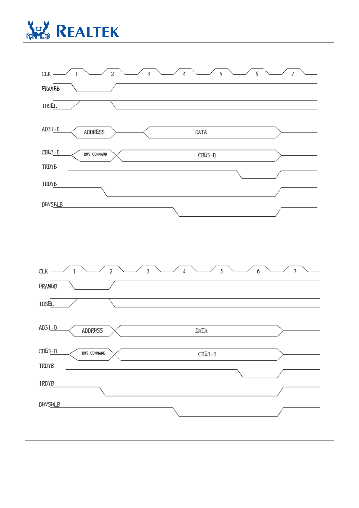
Configuration Read
RTL8100C & RTL8100CL
Datasheet
Configuration Write
Figure 8. Configuration Read
Figure 9. Configuration Write
Single-Chip Fast Ethernet Controller 56 Track ID: JATR-1076-21 Rev. 1.06

Bus Arbitration
RTL8100C & RTL8100CL
Datasheet
Figure 10. Bus Arbitration
Memory Read
Figure 11. Memory Read
Single-Chip Fast Ethernet Controller 57 Track ID: JATR-1076-21 Rev. 1.06
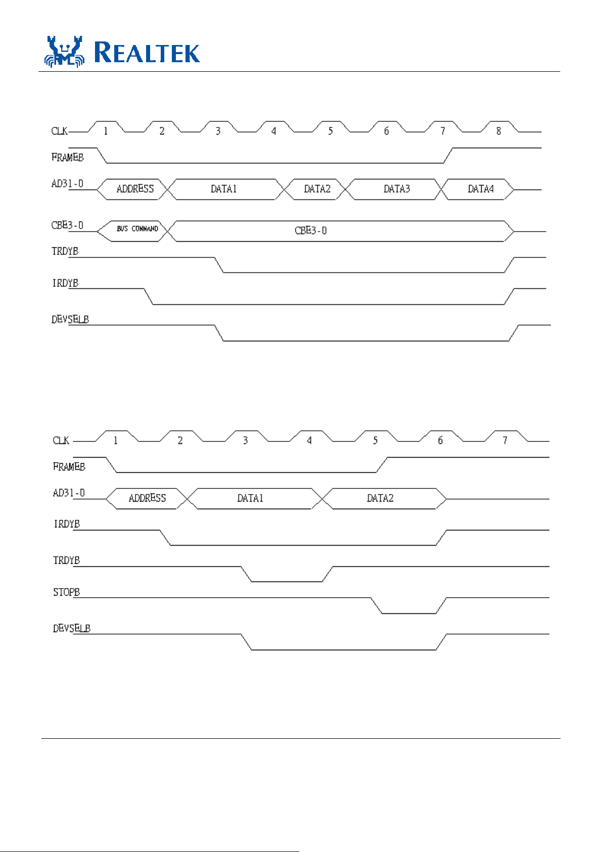
Memory Write
RTL8100C & RTL8100CL
Datasheet
Target Initiated Termination - Retry
Figure 12. Memory Write
Figure 13. Target Initiated Termination - Retry
Single-Chip Fast Ethernet Controller 58 Track ID: JATR-1076-21 Rev. 1.06

Target Initiated Termination - Disconnect
Figure 14. Target Initiated Termination - Disconnect
RTL8100C & RTL8100CL
Datasheet
Target Initiated Termination - Abort
Figure 15. Target Initiated Termination - Abort
Single-Chip Fast Ethernet Controller 59 Track ID: JATR-1076-21 Rev. 1.06

Master Initiated Termination – Abort
Figure 16. Master Initiated Termination – Abort
Parity Operation - One Example
RTL8100C & RTL8100CL
Datasheet
Figure 17. Parity Operation - One Example
Single-Chip Fast Ethernet Controller 60 Track ID: JATR-1076-21 Rev. 1.06

9. Application Information
RTL8100C & RTL8100CL
Datasheet
EEPROM
LED
RJ-45
Magnetics
Figure 18. Application Information
RTL8100C(L)
Auxiliary Power
PCI INTERFACE
CLK
Single-Chip Fast Ethernet Controller 61 Track ID: JATR-1076-21 Rev. 1.06

10. Mechanical Dimensions
10.1. RTL8100C 128-Pin QFP
RTL8100C & RTL8100CL
Datasheet
See the Mechanical Dimensions notes on the next page.
Single-Chip Fast Ethernet Controller 62 Track ID: JATR-1076-21 Rev. 1.06

10.2. Notes for RTL8100C 128-Pin QFP
Symbol Dimension in inch Dimension in mm
Min Type Max Min Type Max 2. Dimension b does not include dambar rotrusion/intrusion.
A
A1
A2
b
c
D
E
e
HD
HE
L
L1
y
θ 0°
- - 0.134 - - 3.40
0.004 0.010 0.036 0.10
0.102 0.112 0.122 2.60
0.005 0.009 0.013 0.12
0.002 0.006 0.010 0.05
0.541 0.551 0.561 13.75
0.778 0.787 0.797 19.75
0.010 0.020 0.030 0.25
0.665 0.677 0.689 16.90
0.902 0.913 0.925 22.90
0.027 0.035 0.043 0.68
0.053 0.063 0.073 1.35
- - 0.004 - - 0.10
-
12° 0°
0.25
2.85
0.22
0.15
14.00
20.00
0.5
17.20
23.20
0.88
1.60
-
0.91
3.10
0.32
0.25
14.25
20.25
0.75
17.50
23.50
1.08
1.85
12°
1. Dimension D & E do not include interlead flash.
3. Controlling dimension: Millimeter
4. General appearance spec. should be based on final visual
inspection spec.
TITLE: 128 QFP (14x20 mm) PACKAGE OUTLINE
-CU L/F, FOOTPRINT 3.2 mm
APPROVE DOC. NO. 530-ASS-P004
VERSION 1
PAGE OF
CHECK DWG NO. Q128 - 1
DATE
REALTEK SEMICONDUCTOR CORP.
RTL8100C & RTL8100CL
Datasheet
LEADFRAME MATERIAL :
Single-Chip Fast Ethernet Controller 63 Track ID: JATR-1076-21 Rev. 1.06

10.3. RTL8100CL 128-Pin LQFP
RTL8100C & RTL8100CL
Datasheet
See the Mechanical Dimensions notes on the next page.
Single-Chip Fast Ethernet Controller 64 Track ID: JATR-1076-21 Rev. 1.06

RTL8100C & RTL8100CL
10.4. Notes for RTL8100CL 128-Pin LQFP
Symbol Dimension in inch Dimension in mm
Min Type Max Min Type Max 2.Controlling dimension: Millimeter
A
A1
A2
b
c
D
E
e
HD
HE
L
L1
θ
- - 0.067 - - 1.70 3.General appearance spec. Should be based on final
0.000 0.004 0.008 0.00 - 0.25
0.051 0.055 0.059 1.30
0.006 0.009 0.011 0.15
0.004 - 0.006 0.09 - 0.20 TITLE: 128LD LQFP (14x20x1.4 mm*2) PACKAGE
0.541 0.551 0.561 13.75
0.778 0.787 0.797 19.75
- 0.020 BSC - 0.50 BSC APPROVE DOC. NO. 530-ASS-P004
0.620 0.630 0.640 15.90
0.855 0.866 0.877 21.70
0.016 0.024 0.031 0.45
- 0.039 REF - 1.00 REF DATE
0° 3.5° 9° 0° 3.5° 9°
1.40
0.22
14.00
20.00
16.00
22.00
0.60
1.50
0.29
14.25 -CU L/F, FOOTPRINT 2.0 mm
20.25 LEADFRAME MATERIAL:
16.30 VERSION 1
22.30 PAGE OF
0.75 CHECK DWG NO. LQ128 - 1
1.Dimension b does not include
dambar protrusion/intrusion.
visual inspection spec.
OUTLINE
REALTEK SEMICONDUCTOR CORP.
Datasheet
11. Ordering Information
Part No. Package Status
RTL8100C 128-pin QFP MP
RTL8100CL 128-pin LQFP MP
RTL8100C-LF 128-pin QFP Lead (Pb)-Free MP
RTL8100CL-LF 128-pin LQFP Lead (Pb)-Free MP
Realtek Semiconductor Corp.
Headquarters
No. 2, Industry East Road IX, Science-based
Industrial Park, Hsinchu, 300, Taiwan, R.O.C.
Tel: 886-3-5780211 Fax: 886-3-5776047
www.realtek.com.tw
Single-Chip Fast Ethernet Controller 65 Track ID: JATR-1076-21 Rev. 1.06

 Loading...