

Page 1
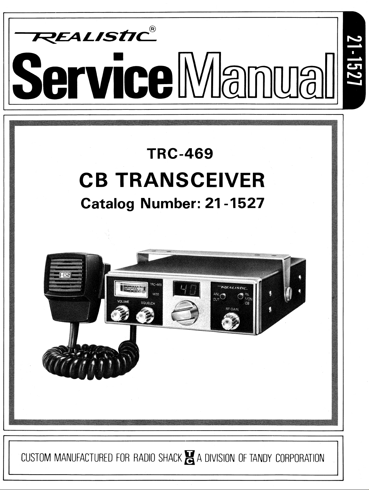
U
TRC-469
•
CUSTOM MANUFACTURED FOR RADIO SHACK M A DIVISION OF TANDY CORPORATION
Page 2
TABLE OF CONTENTS
1.
SPECIFICATIONS
2.
DISASSEMBLY INSTRUCTIONS
BLOCK DIAGRAM
3.
4.
CIRCUIT DESCRIPTIONS
PLL CIRCUIT
AMC CIRCUIT
RF ATTENUATOR CIRCUIT
5.
ALIGNMENT INSTRUCTIONS
6.
TROUBLE SHOOTING HINTS
7.
IC, TR, DIODE & LED LEAD IDENTIFICATION
8.
IC AND COMPOUND PARTS INTERNAL DIAGRAMS
9.
FLEXIBLE P.C. BOARD(TOP VIEW)
10.
SWITCH P.C. BOARD(ANL, PA-MON-CB)
11.
MAIN P.C. BOARD(TOP VIEW)
12.
MAIN P.C. BOARD(BOTTOM VIEW)
13.
ADDITIONAL PARTS ON THE BOTTOM
3 4
5
6
7 10
7 9
10
10
11 - 14
14 16
17
18
19
19
20
21
22
14.
WIRING DIAGRAM
15.
ELECTRICAL PARTS LIST
16.
MECHANICAL PARTS LIST
17.
SCHEMATIC DIAGRAM
18.
EXPLODED VIEW
SEPARATE SHEET
SEPARATE SHEET
24 - 32
33'34
23
Page 3
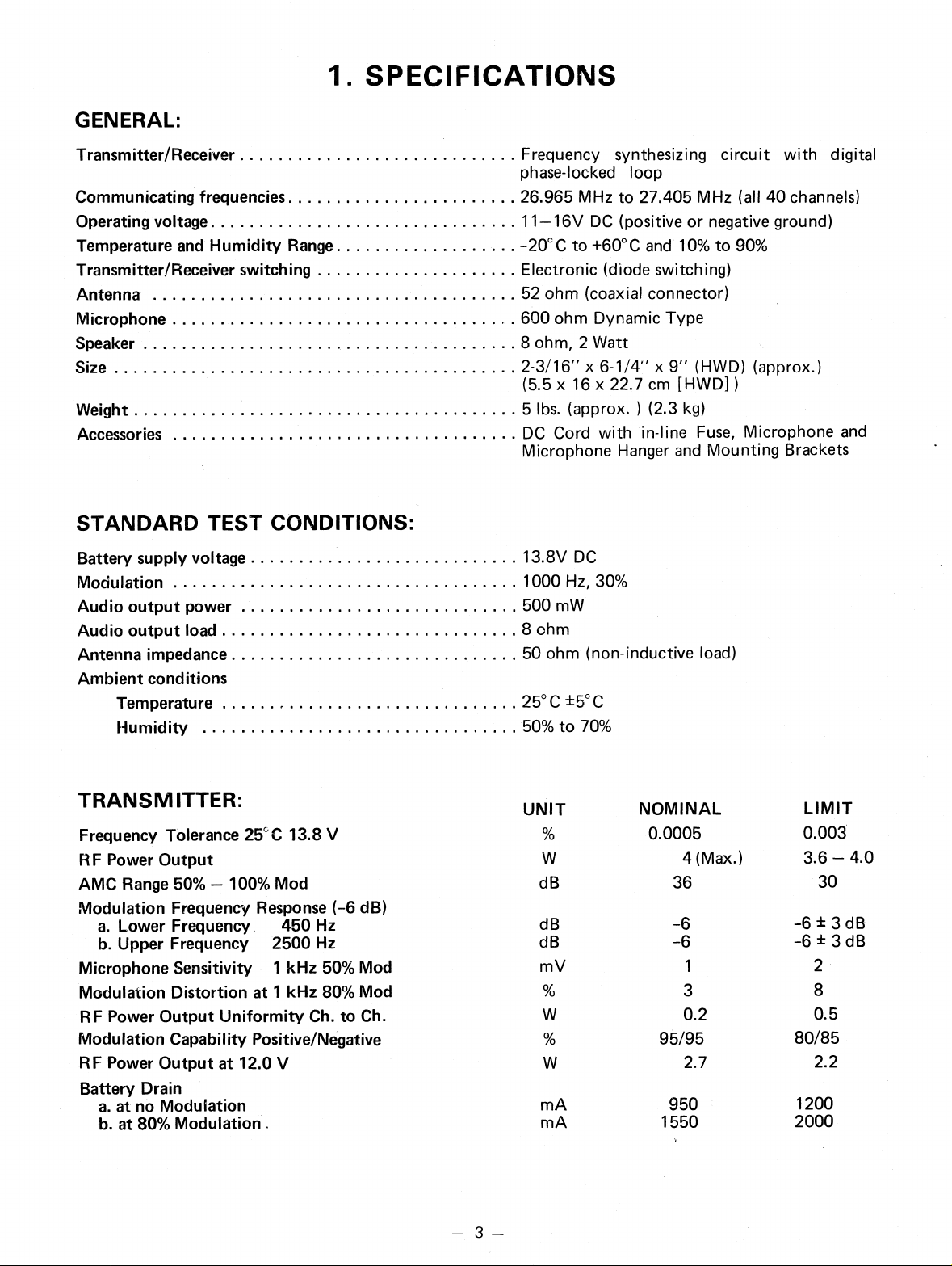
1. SPECIFICATIONS
GENERAL:
Transmitter/Receiver
Communicating frequencies
Operating voltage
Temperature and Humidity Range
Transmitter/Receiver switching
Antenna
Microphone
Speaker
Size
Weight
Accessories
STANDARD TEST CONDITIONS:
Frequency synthesizing circuit with digital
phase-locked loop
26.965 MHz to 27.405 MHz (all 40 channels)
11-16V DC (positive or negative ground)
-20°C to +60° C and 10% to 90%
Electronic (diode switching)
52 ohm (coaxial connector)
600 ohm Dynamic Type
8 ohm, 2 Watt
2-3/16" x 6-1/4- x
(5.5x 16 x 22.7 cm [HWD])
5 lbs. (approx. ) (2.3 kg)
DC Cord with in-line Fuse, Microphone and
Microphone Hanger and Mounting Brackets
(HWD) (approx.)
Battery supply voltage
Modulation
Audio output power
Audio output load
Antenna impedance
Ambient conditions
Temperature
Humidity
TRANSM ITTER:
Frequency Tolerance 25°C 13.8 V
RF Power Output
AMC Range 50% — 100% Mod
Modulation Frequency Response (-6 dB)
Lower Frequency
a.
Upper Frequency 2500 Hz
b.
Microphone Sensitivity 1 kHz 50% Mod
Modulation Distortion at 1 kHz 80% Mod
RF Power Output Uniformity Ch. to Ch.
Modulation Capability Positive/Negative
RF Power Output at 12.0 V
Battery Drain
at no Modulation
a.
at 80% Modulation .
b.
450 Hz
13.8V
1000 Hz, 30%
500 mW
8 ohm
50 ohm (non-inductive load)
25°C ±5°C
50% to 70%
UNIT
W
dB
dB
dB
mV
W
W
mA
mA
DC
NOMINAL
0.0005
4 (Max.)
36
-
6
-
6
1
3
0.2
95/95
2.7
950
1550
LIMIT
0.003
3.6 — 4.0
30
6 ± 3 dB
6 ± 3 dB
-
2
8
0.5
80/85
2.2
1200
2000
3
Page 4

RECEIVER:
(ANL: OUT)
UNIT
NOMINAL
LIMIT
Maximum Sensitivity
Sensitivity for 10 dB S/N
AGC Figure of Merit 50 mV
Overload AGC 50 mV — 1 V
Squelch Sensitivity at Threshold
Squelch Sensitivity at Tight
Adjacent Channel Selectivity
a. at ±10 kHz
Spurious Radiation
Spurious Response Attenuation
a. 455/2 kHz
Image Rejection Ratio
a. -910 kHz
IF Rejection Ratio
a.
10.695 MHz
b.
455 kHz
Cross Modulation
Desensitization (3 dB Desens.)
at 100 pV
Audio Power Output
a.
Maximum
b.
10% THD
Audio Frequency Response (-6 dB)
a.
Lower Freq.
b.
Upper Freq.
THD at 500 mW Audio Output
a.
Input 1 mV 30% Mod
b.
c.
Signal-to-Noise Ratio at 1000 pV
RF Gain Control Range
S-Meter Sensitivity at "S9"
Oscillator Drop-out Voltage
Battery Drain
a.
at no signal
b.
at Max. AF Output
450 Hz
2500 Hz
50% Mod
80% Mod
pV
p
V
dB
dB
p
V
pV
dB
dB
dB
dB
dB
dB
dB
dB
W
W
dB
dB
%
%
%
dB
dB
p V
V
mA
mA
0.3
0.5
90
+4
1000
70
80
80
90
90
115
60
60
-6
-6
45
40
100
250
800
0.25
5
4
2
4
6
7
0.5
1
80
+6
-2
2
355 — 2820
60
60
60
70
80
90
50
55
4
3
-6 ± 3 dB
-6 ± 3 dB
4
6
8
35
30
50 — 200
10
600
1500
PUBLIC ADDRESS:
Microphone Sensitivity for 4 W
Output Power at 1 kHz
Power Output
Maximum
a.
b.
10% THD
Audio Freq. Response (-6 dB)
a.
Lower Frequency
b.
Upper Frequency
Battery Drain
a.
at no signal
b.
at Max. AF Output
450 Hz
2500 Hz
4
mV
W
W
dB
dB
mA
mA
-6
-6
300
1000
4
5
4
10
4
3
-6 ± 3 dB
-6 ± 3 dB
700
1500
Page 5
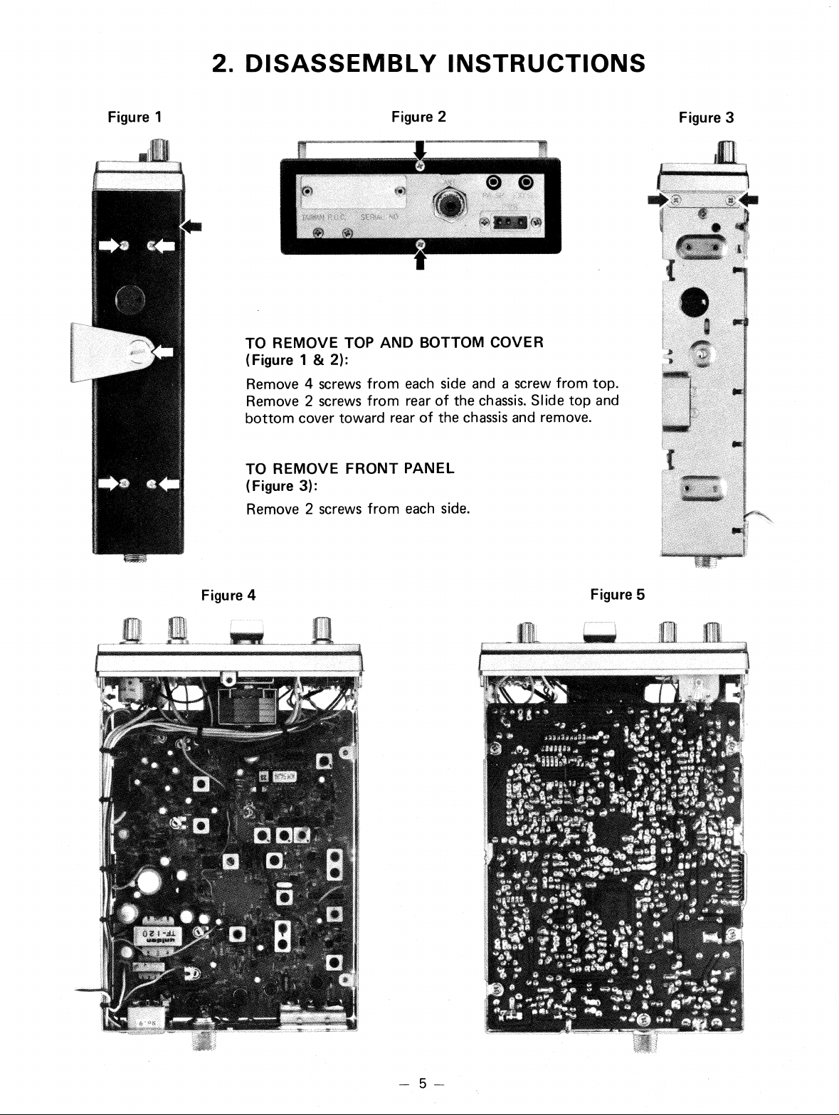
2. DISASSEMBLY INSTRUCTIONS
Figure 1
Figure 2
Figure 3
t
TO REMOVE TOP AND BOTTOM COVER
(Figure 1 & 2):
Remove 4 screws from each side and a screw from top.
Remove 2 screws from rear of the chassis. Slide top and
bottom cover toward rear of the chassis and remove.
TO REMOVE FRONT PANEL
(Figure 3):
Remove 2 screws from each side.
Figure 4
Figure 5
Page 6
ci
co
_ii
O
0
Ei
<
C7
ce
Q
Page 7
4. CIRCUIT DESCRIPTIONS
PLL CIRCUIT:
The PLL circuit used in TRC-469 consists of 7
major parts: Voltage Controlled Oscillator(VCO),
1/N Divider, Phase Detector, Low Pass Filter,
[FVCO[ BY TP-1
12.279: 12.7202
RX
TR22
TX 16.725 — 17.165 MHz [TX. MIXER}
BUFFERI
IC3
V.C.O.
BUFFER
12C1Li
a.
BY TR14
COLLECTOR
RX 16.270-16.710 MI
TR14
TX 16.72517.165 MHI"
[F1I BY TP-3
RX 910 ^ 1,350 kHz
TR15
MIXER
t__
TX 1,365 — 1,805 kHz
Reference Oscillator (10.24 MHz), 1/2048 divider
and Code Converter ROM(Read Only Memory).
[Fstc1)
15.360 MHz
.120 MHz
L19
r
I
1>
IS Amp
3.8V
3.5V
1.5V
1.2V
CH1
TP2
0
RX = H
TR13
TX/RX
SW
TX = L
IC 4
PIN NO.
WAVE
FORM
IC4
PIN NO.
WAVE
FORM
NOTE:
22
21, 20, 7
+2.8V
+2.8V
+1.4V
RX . 910
—
1,350 kHz
TX = 1,365 — 1,805 kHz
c
.
,_______
10k4
CH
CH 1
H
CH 18
L
t
CH 23
H H
1
CH 40
L L L L
SCOPE WAVE FORMS FOR LEVEL REFERENCE
H = High (3.5V — 5 V)
L = Low (0V — 1V)
PIN NO. 1 through 4,5, & 6 are as in program
input data chart.
,
CH23
CH40
Filter
—
WAVE FORM OF IC 4
18,17
DV
2
18
L
L L
2.4V DC
—2.4V
19
3
1C
L
L
aVDC1 v
4
10
L
H
L
16,11
5V DC
15
H
=
LOCKED
L=
UNLOCKED
where
H
.
3.5
—
5V
L=
0
0 .
.= 1.0V
5
6
2A
2B
L
L
H
L
H
L
L
L
5.0V
3.5V
ov Low
IC4
13
10.240 MHz
9
H= RECEIVE
L = TRANSMIT
Where
FI = 3.5 — 5V
L = 0 — 1.0V
_
High
RX
TX
4.8V P.P.
10
12
10.240 MHz
5.120 MHz
V
ilter Amp
PHASE
DETECTOR
C.P
PROGRAMMABLE DIVIDER 10 Bit
t
0
CHANNEL SELECTOR
.*12
k
5 kHz
SW
CODE CONVERTER
(ROM)
000
SWITCH
Hz
11 Bit DIVIDER
1/2,043
t
T Q
REF. OSC
V DD
V DC V DD
KEYING RX = 8V
The VCO is an oscillator which controls oscillation
frequency in accordance with input voltage change.
The VCO output is mixed with a signal in the
transmitter or receiver circuitry. A portion of the
5V P.P.
VCO frequency is fed through TR14 Buffer Amp
--
and then added to TR 15. This frequency is mixed
with a 15.36 MHz frequency then goes to IC4
(1/N divider).
"N" for the 1/N divider is determined by Channel
4V P.P.
Selector Switch whose output is selected by a Code
Converter ROM.
As shown in the frequency chart, N is different
between transmit and receive mode since only one
crystal is used with this PLL circuitry.
The output from the 1/N divider is fed to Phase
Detector. On the other hand, the frequency
from the Reference OSC, 10.24 MHz, is divided
to 5 kHz by 1/2048 divider and applied to another
input of Phase Detector.
0-J
TX = CV
Page 8
The Phase Detector detects the difference of these
two input signals and produces a voltage which
controls the VCO frequency.
The Low Pass Filter integrates the output of the
Phase Detector which controls the VCO frequency
and the 1/1\1 divider produces a 5 kHz frequency.
Thus the Phase Detector receives two input signals
(both 5 kHz). It compares the phase difference
between the two, generating an error voltage,
which acts on the VCO to bring the two frequencies exactly in-phase. When this condition occurs,
the PLL circuit is locked.
Fvco (the Frequency of the VCO) is changeable in
10 kHz increments, by varying the program divide
ratio, N.
For example, the divide ratio, N is programmed to
273 for channel No. 1 Transmit; therefore Fvco is
calculated as follows:
Fvco = 15,360 + 5 x 273 = 15,360 + 1,365
= 16,725 (kHz)
In the same manner, Fvco for channel No. 2
through No. 40 is determined as shown in Table A.
Transmitter Local Oscillator
The Transmitter local oscillator frequency of
10.240 MHz is produced by IC4 oscillator, IC4 and
crystal, X'tal 1.
Table A shows Frequency Chart of Fvco and
Divide Ratio vs. Antenna Frequency, and Program
input data.
CIRCUIT FOR DETERMINING
FREQUENCY:
Output Frequency of the Transmitter
Transmit frequency, Ft, is taken from the output
of the Transmitter Mixer IC1.
One of the inputs of IC1 is the 1st local frequency,
Fvco, which is produced by the PLL Local
Oscillator circuit. The other input is the transmitter local oscillator frequency of 10.240 MHz
produced by JC4.
The sum of these frequencies determines the transmit frequency as follows:
Ft = Fvco = 10.240 (MHz)
PLL Local Oscillator
Fvco, the output frequency of the VCO (Voltage
Controlled Oscillator), IC3, is fed to one of the
inputs of the PLL Mixer, TR15.
The offset frequency, Fstd, 15.360 MHz (10.240
MHz = 2 x 3) is fed to another input of TR 15.
The input frequency to the Programmable Divider,
Fl, is calculated as follows:
Channel Selection Program
The divide ratio of the Programmable Frequency
Divider in IC4 is determined through the Code
Converter and Transmit/Receive mode switch in
IC4 by the voltage supplied to the program input
terminals, Pin No. 1 through Pin No. 6 of IC4.
The program input voltage for Pins 1 through 6 is
supplied from the Channel Selector switch accord-
ing to the Channel Number.
The Transmit/Receive mode switch in IC4 changes
the divide ratio of the Programmable Divider by
changing Pin 9 voltage (High level for Receive, Low
level for Transmit), to produce a 455 kHz change
in VCO frequency when changing between the two
modes.
When changing between Receive and Transmit
modes, a varactor diode in the VCO IC, IC3, is
switched in or out, respectively.
The bias voltage on this varactor is so designed that
the VCO control voltage does not change when
switching between modes, thus reducing lock-up
time.
Fl = Fvco + Fstd (15.360 MHz)
F 1 is fed to the Programmable Divider in the PLL
IC, IC4 and divided by N, through the Pro-
grammable Divider.
The 10.240 MHz frequency produced by the Re-
ference Oscillator in IC4 is divided by 2,048 (the
Reference Frequency Divider in IC4) and the
resultant frequency, F2, is:
F2 = 10.240 MHz = 2,048 = 5 kHz
The output frequency of the Programmable Divider is compared with F2 at the Phase Detector in
IC4. When the frequency and phase of these two
signals are precisely the same, the PLL circuit is
"locked".
Therefore, Fvco is determined by the following
formula.
Fvco = Fstd (15,360 kHz) + 5 x N (kHz)
Page 9
CIRCUIT FOR PREVENTION OF UNAUTHORIZED FREQUENCY EMISSION:
This Transceiver has a built-in circuit which prevents transmission of unauthorized frequencies
during the time when the PLL circuit is not locked
or when the Channel Selector switch is between
channels.
When the PLL circuit is not locked or the program
data input is not for channel 1 — 40, pin 15 in IC4
produces a low level digital control signal. This
signal is fed to the base of RF signal Disable
Transistor, TR 16 (INSTANT STOP).
When the Channel Selector is switched from one
input (other than data required for channels
1 — 40). However, between channels, the Channel
Selector produces a control signal at ground
potential, and this signal is fed to the base of
RF signal Disable Transistor, TR 16.
In either case, when the base of TR16 is at low
level, TR16 will not conduct and thus reduces the
supply voltage to the Amplifier stage inside IC1
to zero. This eliminates the RF signal output, and
prevents any transmission on unauthorized fre-
quencies.
channel to another, it may produce a non-valid
TABLE A: FREQUENCY CHART OF Fvco AND DIVIDE RATIO N
Antenna
Frequency
(MHz)
26.965
26.975
26.985
27.005
27.015
27.025
27.035
27.055
27.065
27.075
27.085
27.105
27.115
27.125
27.135
27.155
27.165
27.175
27.185
27.205
27.215
27.225
27.255
27.235
27.245
27.265
27.275
27.285
27.295
27.305
27.315
27.325
27.335
27.345
27.355
27.365
27.575
27.385
27.395
27.405
Channel
Number
1
2
3
4
5
6
7
8
9
10
11
12
13
14
15
16
17
18
19
20
21
22
23
24
25
26
27
28
29
30
31
32
33
34
35
36
37
38
39
40
Divide
Ratio
(N)
273
275
277
281
283
285
287
291
293
295
297
301
303
305
307
311
313
315
317
321
323
325
331
327
329
333
335
337
339
341
343
345
347
349
351
353
355
357
359
361
For Transmit
F1
(kHz)
1,365
1,375
1,385
1,405
1,415
1,425
1,435
1,455
1,465
1,475
1,485
1,505
1,515
1,525
1,535
1,555
1,565
1,575
1,585
1,605
1,615
1,625
1,655
1,635
1,645
1,665
1,675
1,685
1,695
1,705
1,715
1,725
1,735
1,745
1,755
1,765
1,775
1,785
1,795
1,805
VCO
Frequency
(MHz)
16.725
16.735
16.745
16.765
16.775
16.785
16.795
16.815
16.825
16.835
16.845
16.865
16.875
16.885
16.895
16.915
16.925
16.935
16.945
16.965
16.975
16.985
17.015
16.995
17.005
17.025
17.035
17.045
17.055
17.065
17.075
17.085
17.095
17.105
17.115
17.125
17.135
17.145
17.155
17.165
Divide
Ratio
(N)
182
184
186
190
197
194
196
200
202
204
206
210
212
214
216
220
222
224
226
230
232
234
240
236
238
242
244
246
248
250
252
254
256
258
260
262
264
266
268
270
For Receive
F1
(kHz)
910
920
930
950
960
970
980
1,000
1,010
1,020
1,030
1,050
1,060
1,070
1,080
1,100
1,110
1,120
1,130
1,150
1,160
1,170
1,200
1,180
1,190
1,210
1,220
1,230
1,240
1,250
1,260
1,270
1,280
1,290
1,300
1,310
1,320
1,330
1,340
1,350
VCO
Frequency
(MHz)
16.270
16.280
16.290
16.310
16.320
16.330
16.340
16.360
16.370
16.380
16.390
16.410
16.420
16.430
16.440
16.460
16.470
16.480
16.490
16.510
16.520
16.530
16.560
16.540
16.550
16.570
16.580
16.590
16.600
16.610
16.620
16.630
16.640
16.650
16.660
16.670
16.680
16.690
16.700
16.710
1A
Program input data
1B
1C
HL
L
H H
L L
HL
L
H H H
L
HL
L
HL
L
H H
L
HL
L
H
L
HL
L
HL
L
HH
L
HL HL
L
H H
L L
HL
L L
HL
L
H H
L
HL
L
H
Lit_
HL
L
HL
H H
L
L
HL
L
HH
H H
L L
L
HL
L
H
HL
L
HH
H
L
L
L L
HL
HL
L
L
L
L
L
HL
HL
L
L
L L L
L
HL
H
H
L
L
L
L
L
HL
HL
H
L
L
L
1D
L
L
L
L
HL
HL
L
L
L
L
L
L
HH
H
L
L
L
L
L
HL
HL
L
L
L
L
L
L
H
H
L
2A
L
L
L
L L
L
L
L
HL
HL
HL
HL
HL
HL
HL
HL
H
L
L
L
L
L
L
L
H
HH
HH
HH
HH
HH
HH
HH
H
H
L
2B
L
L
L
L
L
L
L
L
L
L
H
H
H
H
H
H
H
H
H
H
H
H
H
L
Page 10
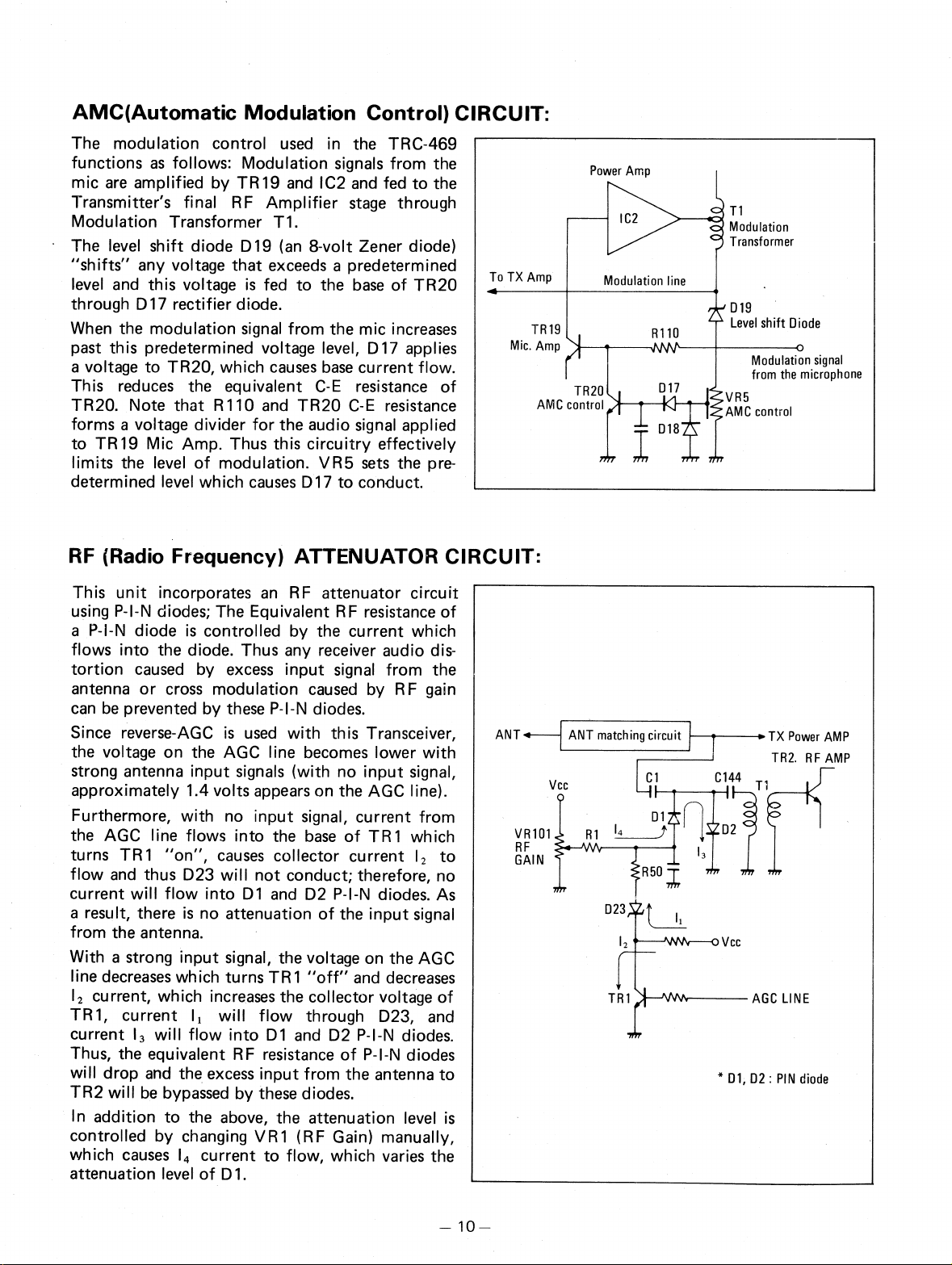
AMC(Automatic Modulation Control) CIRCUIT:
The modulation control used in the TRC-469
functions as follows: Modulation signals from the
mic are amplified by TR19 and IC2 and fed to the
Transmitter's final RF Amplifier stage through
Modulation Transformer Ti.
The level shift diode D19 (an 8-volt Zener diode)
"shifts" any voltage that exceeds a predetermined
level and this voltage is fed to the base of TR20
through D17 rectifier diode.
When the modulation signal from the mic increases
past this predetermined voltage level, D17 applies
a voltage to TR20, which causes base current flow.
This reduces the equivalent C-E resistance of
TR20. Note that R110 and TR20 C-E resistance
forms a voltage divider for the audio signal applied
to TR 19 Mic Amp. Thus this circuitry effectively
limits the level of modulation. VR5 sets the pre-
determined level which causes D17 to conduct.
RF (Radio Frequency) ATTENUATOR CIRCUIT:
To TX Amp
TR19
Mic. Amp
AMC control
Power Amp
IC2
Modulation line
TR20
R110
sMAP
D17
— D18
T1
Modulation
Transformer
D19
Level shift Diode
0
Modulation signal
from the microphone
VR5
AMC control
This unit incorporates an RF attenuator circuit
using P-I-N diodes; The Equivalent RF resistance of
a P-1-N diode is controlled by the current which
flows into the diode. Thus any receiver audio distortion caused by excess input signal from the
antenna or cross modulation caused by RF gain
can be prevented by these P-I-N diodes.
Since reverse-AGC is used with this Transceiver,
the voltage on the AGC line becomes lower with
strong antenna input signals (with no input signal,
approximately 1.4 volts appears on the AGC line).
Furthermore, with no input signal, current from
the AGC line flows into the base of TR 1 which
turns TR1 "on", causes collector current 1
flow and thus D23 will not conduct; therefore, no
current will flow into D1 and D2 P-I-N diodes. As
a result, there is no attenuation of the input signal
from the antenna.
With a strong input signal, the voltage on the AGC
line decreases which turns TR1 "off" and decreases
1
2
current, which increases the collector voltage of
TR1, current I
current 1
3
will flow into D1 and D2 P-I-N diodes.
1
will flow through D23, and
Thus, the equivalent RF resistance of P-I-N diodes
will drop and the excess input from the antenna to
TR2 will be bypassed by these diodes.
In addition to the above, the attenuation level is
controlled by changing VR1 (RF Gain) manually,
which causes 1
4
current to flow, which varies the
attenuation level of Dl.
2
to
ANT 4
VR101
RF
GAIN
ANT matching circuit
Vcc
TR1
Cl
*TX Power AMP
TR2. RF AMP
C144
T1
AGC LINE
* D1, D2 : PIN diode
Page 11

5. ALIGNMENT INSTRUCTIONS
CHASSIS LAYOUT-ALIGNMENT POINTS:
Page 12

ALIGNMENT OF PLL PORTION:
1. Test Equipment Required
a.
Oscilloscope (0 — 50 MHz)
b.
Frequency Counter (0 — 50 MHz)
c.
DC Volt Meter (10 Volts maximum, 100K ohm/Volt)
d.
50 ohm Load
e.
DC Power Supply (13.8 V/2-Amp)
2. Alignment Procedure (See Pages 7 and 11)
Step
1
2
3
4
5
Preset to
Receiver mode ,
Channel 40
Same as step 1
Same as step 1
Same as step 1
Same as step 1
Oscilloscope to
secondary of L21
(TP4)
Frequency Counter
to secondary of
L21 (TP4)
Frequency Counter to
Pin 22 of IC4
(TP3)
DC Volt Meter to
Pin No. 4 of IC3
(TP2)
Frequency Counter
to secondary of L17
(TP1)
PLL TEST EQUIPMENT SETUP
Connections
Adjustment
L21
VC1
L19
L18
VC1
Remarks
Adjust L21 for the
maximum indication
on Oscilloscope.
Adjust VC1 to obtain
10.240 MHz indication.
Adjust L19 to obtain
15.360 MHz indication.
Adjust L18 to obtain
approx. 3.50V reading.
Adjust VC1 for
16.710000 MHz.
— 12
Page 13

ALIGNMENT OF TRANSMITTER PORTION:
1. Equipment Required
VTVM (full scale: 1V DC with RF Probe)
a.
b.
RF Output Power Meter
c.
Turnable Field Strength Meter
(Wave Meter or Spectrum Analyzer)
d.
Frequency Counter (0 — 30 MHz)
2. Procedure (See Page 11)
e.
DC Power Supply (13.8V/2—Amp)
f.
50 ohm Load and Attenuator
g.
Oscilloscope (0 — 30 MHz)
h.
AF Oscillator
Step
1
2
3
4
5
6
8
Preset to
TX Mode,
No Modulation,
Channel 19
Same as step 1
Conditions
RF Output Power
Meter to ANT. Jack
J101. VTVM to TP5
RF Output Power
Meter to ANT. Jack
J101
Alignment
L15,16,17,
21
L11,13,14
Remarks
Adjust for a maximum
indication on VTVM.
Adjust for a maximum
indication on RF
Output Power Meter.
Adjust to obtain
Same as step 1
Same as step 2
L11
Nominal 3.8 W of
RF Output Power.
Tunable Field Strength Meter
Same as step 1
to Ant. Jack (J101) through
a suitable load and attenuator
(Use Spectrum Analyzer if
L8
Adjust for minimum
2nd Harmonic Output.
available)
Repeat above adjustments, until no further change can be noted.
TX Mode,
Ch19, 1 kHz
100mV
applied to Mic
Input for MOD
Audio Generator to Pin 4 of
Microphone Jack (J3).
Oscilloscope to ANT.
Jack (J101) through a
suitable load and attenuator
VR5
Adjust for 95%
Modulation.
Check that RF Output
RF Output Power
7
Same as step 1
Meter to Ant. Jack
VR4
J101
Power Meter reads
3.8W, then adjust
VR4 so that the Transceiver's Meter just approaches the 4 mark.
TX Mode,
No Modulation,
All channels
Frequency Counter to
Ant. Jack (J101) through
a suitable load and
attenuator
Check Frequency of
all channels.
TRANSMITTER TEST EQUIPMENT SETUP
Pi-n 4
TRC-469 Transceiver
AF
Oscillator 0-4
Si
MIC
JACK
-7(
AF VTVM
DC Supply 13.8V
00
RF Power meter
5012 Load
Attenuator
Oscilloscope I
1-1:36;r:
,-
73
Frequency
Counter
-J
Spectrum Analyzer
0 0
=1
00
000
_J
Page 14

ALIGNMENT OF RECEIVER PORTION:
1. Equipment Required
a.
Signal Generator (27 MHz Band, 1000 Hz, 30%
AM Modulation, Output Impedance = 50 ohm)
Audio VTVM
b.
2. Procedure (See page 11)
Oscilloscope
c.
Dummy Load (8 ohms, 5 watts, resistive)
d.
DC Power Supply (13.8 V, 2 Amp.)
e.
Step
1
2
3
4
SG Connection:
Frequency
To Ant. Connector
(J101)
Freq: 27.185 MHz
Same as ste 1
Same as step 1
Same as step 1
p
Preset to
Channel 19
Volume: Max.
Squelch: Min.
Same as
step 1
Volume: Max.
Squelch: Max.
Same as
1
p
ste
RECEIVER TEST EQUIPMENT SETUP
Audio
VTVM
To EXT.
SPK.
Jack(J2)
Same as
step 1
Same as
step 1
Same as
step 1
Adjustment
L1,2,3,4,5,
6,7
V R1
VR2
(Squelch)
VR3
Remarks
Adjust for a max.
Audio Output
Adjust for 2 V output with
SG level of 0.3µV
Adjust
f
SG output level of 1000µV.
Adjust for a reading of S-9 on
the Transceiver's S-meter with
SG output level of 100 i.tV.
or
:, V
output with
8E2
Resistor
UNIT WILL NOT TURN ON
1.
Defective Power Switch
2.
Blown Fuse
Defective Power Switch
3.
Defect in Power Supply circuitry
4.
NO RECEIVE SOUND
1.
Defective external speaker jack
2.
Bad contact in the microphone jack
Bad PTT switch in the microphone
3.
4.
Unlocked PLL circuitry
Defect in Squelch circuitry
5.
Defective PA-MON-CB switch
6.
6. TROUBLESHOOTING HINTS
NO TRANSMIT
Defective Microphone jack
1.
2.
Defective PTT switch on Microphone
Off-tuned main or local Oscillator
3.
4.
Defective PA-MON-CB switch
NO TX MODULATION
1.
Defective microphone and/or circuitry
2.
Defect in Modulation circuitry
Page 15

FOR MORE HINTS, SEE BELOW
(Also Refer to Pages 7-10)
NO TRANSMIT
A.
Connect current meter in series with power
cable and check the current reading for transmit mode:
If current reads more than 1 ampere (but less
than 2 A.), it means the final output transistor is OK, so check for bad contacts or
short circuits between PC Board and Antenna
Connector. If current reads less than 0.5A: it
indicates there is no drive to Final Transistor,
so check drive or early RF stages.
B.
Defective PLL ?
Check if voltage at the emitter of TR 16 is less
than 3 Volts. If less than 3V then PLL is un-
locked or Channel Selector Switch is between
Channels. If more than 3V then PLL is OK.
Short Circuit in Transmitter Circuitry ?
C.
Voltage at emitter of TR21 should be less than
7 Volts (TX mode) should increase to more
than 7 Volts in RX mode.
D.
If voltage reading is more than 7 Volts at the
collector of TR18, problem is not here. If
voltage of more than 2 Volts is measured
between R101 and D16, then check microphone circuitry or D16 diode.
If RF voltage (27 MHz) is more than 200 mV
E.
P-P at TP-5, previous stages are OK.
F.
No voltage readings at collector of TR 10 and
TR 11: check D11 or T-1.
G.
No Channel LED light: If one particular
segment does not light, the problem is with the
entire LED or a bad contact in the Channel
Selector Switch or a broken Flexible Printed
Circuit. If LED does not light in any channel
position, check D14 or FPC. With a defective
FPC, transmit will not operate.
NO CHANNEL LED LIGHT
If one particular channel does not light, check
Flexible Printed Circuit Board or LED itself or
Channel Selector Switch.
If no channel lights, check D16 diode or socket
for Flexible Printed Circuit Board.
NO TX MODULATION
If receiver operates correctly but with no modula-
tion on TX, then problem should be TR 19, TR20
or short circuit in the microphone circuitry, since
audio power IC2 is used for both TX and RX
modes.
NO RECEIVE
Before trouble shooting, be sure that Squelch
Control is fully CCW and microphone is connected.
A) Connect Signal Generator to antenna and see if
Signal Strength Meter (5 meter) deflects:
S meter deflects:
Antenna through IF stage should be all right;
check the circuit through ANL, Squelch and
Audio amplifier. During the deflection of S
meter, negative voltage should be present at
cathode of D6 diode if Detector circuit is
normal.
S meter does not deflects:
To determine whether PLL is OK, check
following:
1.
A frequency in the range of 16 MHz should
be present at TP-1 (0.5V P-P or more).
2.
The frequencies shown on page 11 should be
correct when Channel Selector Switch is
changed from CH 1 through CH 40.
3.
A frequency of 10.24 MHz should be present at TP 4 (0.2V P-P or more). If PLL is
OK, then check circuitry through TR6, TR5,
TR4, TR3, TR2 and TR1.
B) Check whether Audio stage operates: Connect
Speaker to PA Speaker Jack and set PA-CB
switch to PA position. If click noise is audible
when PTT switch is pressed, Audio Stage is
OK. If no click noise, IC2 Audio Amplifier is
defective or bad T-1 Transformer. (Transformer DC resistance should be approximately
0.5 ohm for both primary and secondary
windings.)
C) Defective Audio Power IC ?
If voltage reading at pin 10 = 7V (VCC/2), IC2
should be all right.
D) Squelch is on all the time
TR7 is defective if voltage at the collector of
TR8 is more than 5 volts. If reading is less
than 2 volts, check TR9 circuitry and/or
Squelch control's ground connection for cold
solder.
Page 16

PLL CIRCUIT TROUBLESHOOTING HINTS
(also Refer to Page 7):
N
Check whether voltage
reading on Pin 1 of IC3 is
approx. 5.1 volts.
Defective Vcc line (5V).
Check whether there is RF
output of approx. 0.2
V P-P at secondary of L19.
Check whether there is RF
voltage(0.2Vp-p) on Pin 2 of
IC3.
Yes
Defective IC3, L18 open or
poor soldering.
Defective Switch.
Defective Flexible PCB or
Connector J4.
Yes
V
4, Yes
Defective TR22, L17
or poor soldering.
No
Defective TR15 or
poor soldering.
No good
Check whether there is RF
voltage on TP1.
(
Check whether BCD
programs on Pin 1 thru 6 of
IC4 are as specified in the
Chart.
0
Check for RF signal
of 16 17 MHz at
collector of TR14.
Yes
Yes
Check for RF signal
of 0.9 — 1.8 MHz
on TP3.
Yes
Yes
Check whether there is approx.
volts at CH1 and 3.5 volts at CH40
on TP2.
Yes
Check whether each Channel
Frequency matches the frequency
indicated in Frequency Chart.
Yes
Check whether voltage
is 3.5 volts on TP2 at
CH40.
Check whether voltage
reading on Pin 8 of IC3 is
approx. 2.5V on RX and
5.0V on TX.
Re-align L18.
4,
Yes
Defective IC4.
good
PLL is not
detective
A
1.8
Yes
Check whether there is
Output of 5.120 MHz on
Pin 10 of IC4.
Defective L19 or poor
soldering.
Defective Crystal, or IC4
or poor soldering.
Yes
Defective TR14 or 1C3
or poor soldering.
Defective TR13 or
poor soldering
Page 17

7. IC, TRANSISTOR, DIODE & LED LEAD IDENTIFICATION
IC-1 TA7310P
TAPERED
Ec
ECB
MARKING
SIDE
MARKING SIDE
9
TR-1,7,9,13,16,19,20
2SC458
TR-12
2SC2076
MARKING
SIDE
IC-2 MB3710
B C E
MARKING SIDE
10
TR-3,4,5,6,14,15,22
2SC460
TR-8,17,18
2SA844
TR-2
2SC1342
IC-3 UHIC006
V
BCE
TR-10
TR-21
10
10
2SC2029
2SC1419
MARKING
SIDE
IC-4 KM5624
22
12
22
TR-11
ECB
2SC2029
MARKING
12
11
SIDE
1 2 3
D-201 TLR321
16
0 0 0 0
0 0
0 0
0 0
0 0
1------8
4
T TT
13 14 15 16
9
0 0
0 0
6 7 8 9 10 11 12
LR0702R
CATHODE
L-101
ANODE
AF
CATHODE
I
---
ANODE
D-9,10,12,15,16,24
1S2076
D-1,2
MC301
F
D-11,22
SR1K1
D-5,6,7,8,17,18,25
1N60AM
iDN
3
60
4
p
D-20,21,19 XZ086
D-13,23 XZ051
D14
BZ052
Page 18

8. IC & COMPOUND PARTS INTERNAL DIAGRAMS
IC-1, TA7310P
IC-2, MB3710
- 1 8 -
Page 19

RR 2
x 7 HA-013
,
1:K
9. FLEXIBLE P C. BOARD(TOP VIEW)
:``
w
-J
U)
10. SWITCH P.C. BOARD (ANL, PA-MON-CB)
S101
R115
-400 1/2 W
Page 20

11. MAIN P.C. BOARD (TOP VIEW)
- 20 -
Page 21

12. MAIN P.C. BOARD (BOTTOM VIEW)
21
Page 22

13. ADDITIONAL PARTS ON THE BOTTOM
Page 23

14. WIRING DIAGRAM
JI01
5P 101
SPI
N
VR101
LRF GAIN
50
KB
W30 BLK 3 - 60-3
Page 24

REVISION
FOR
AUSTRALIAN MODEL OF TRC-469
Catalog Number: 21-9469
When servicing Australian model of TRC-469(Catalog Number 21-9469),
refer to the Service Manual for TRC-469(Catalog Number 21-1527) as
well as the following revision:
1. SPECIFICATIONS
Page 3
GENERAL:
27.225 MHz
to
90%
85%
to
+50°C
and
Communicating Frequencies
Temperature and Humidity Range
STANDARD TEST CONDITIONS:
Ambient conditions Humidity
27.015 MHz
(All 18 channels)
-30°C
10%
to
45%
to
Page 8
Page 9
The 4th paragraph should be as follows:
for channel
For example, the divide ratio, N is programmed to
No.1 Transmit, therefore Fvco is calculated like this;
283
Fvco = 15.360 + 5 x 283 =15.360 + 1415
= 16.775 (kHz)
In the same manner, Fvco for channel No.2 through No:18 is
determined as shown in Table A.
The 2nd and 3rd paragraphs should be as follows:
When the PLL circuit is not locked or the program data input is
18,
not for channel 1 —
control signal. This signal is fed to the base of RF signal Disable
Transistor, TR-16 (INSTANT STOP).
When the Channel Selector is switched from one channel to
another, it may produce a non-valid input (other than data
required for channels 1 —
Channel Selector produces a control signal at ground potential,
and this signal is fed to the base of RF signal Disable Transistor,
TR 16.
Refer to the attached revision of
pin 15 in IC4 produces a low level digital
However, between channels, the
18).
TABLE A: FREQUENCY
CHART OF Fvco AND DIVIDE RATIO N.
BLOCK DIAGRAM
3.
Page 6
Refer to the attached revision.
CIRCUIT DESCRIPTIONS
4.
Page 7
Refer to the revised PLL circuit diagram attached.
The frequencies in the WAVE FORM IC4, pin No.22 should be
Rx = 960 kHz — 1170 kHz, Tx = 1415 kHz — 1625 kHz.
ALIGNMENT INSTRUCTIONS
5.
Page 12
2. ALIGNMENT PROCEDURE
Step 1, Preset to: Receive mode, channel
Step 4, Remarks: Adjust L18 to obtain approx.
Step 5, Adjustment: L17, Remarks: Adjust
18.
L17
2.50V
for
reading.
16.530000 MHz.
Page 13
2. ALIGNMENT PROCEDURE
The channel number in step 1 and 6 should be Channel
10.
Page 25

Page 14
15.
ELECTRICAL PARTS LIST
2. ALIGNMENT PROCEDURE
Step 1, SG Connection Frequency: 27.125 MHz, Preset to:
Channel 10.
6. TROUBLESHOOTING HINTS
Page 15
S METER DOES NOT DEFLECTS: The channel No.40 in item 2
should read as channel 18.
Page 16
The first and third clauses from top-right hand side should be as
follows:
Check whether there is approx. 1.8 volts at CH 1 and 2.5 volts at
CH18.
Check whether voltage is 2.5 volts on TP2 at CH18.
IC, TRANSISTOR, DIODE &
LED LEAD IDENTIFICATION:
Page 17
The type number of IC-4 should be KM5626 Lead designation is
same as KM5624.
8. IC & COMPOUND PARTS INTERNAL DIAGRAMS
Page 18
The type number of IC-4 should be KM5626 and refer to the
revised block diagram attached.
The resistor compound parts RR-1, HA-014 and RR-2, HA-013
should be deleted.
Page 26
Delete C-102, Ceramic Capacitor
Page 27
Add C-202 Ceramic Capacitor, 0.01/IF 25V K SL
Add C-203 Ceramic Capacitor, 0.01/IF 25V K SL
Read type number of IC-4 as IC, KM5626
Page 30
Add R-201 Carbon Film Resistor, 1K-ohm 1/8W J RFPZ181024
Add R-202 Carbon Film Resistor, 1K-ohm 1/8W J RFPZ181024
Read type number of S-201 Rotary Switch as SR-198
MECHANICAL PARTS LIST
16.
Page 33
Add Pan Head Screw 3 x 8 for TR11
Page 34
Delete Bracket for Meter, F.C.C. Plate and Binding Screw M3 x 6
for speaker.
Add:
Spring Washer 2.6 diameter
Hexagonal Nut M2.6
Name Plate(rear of the chassis)
Binding Screw M2.6 x 6
CKGZ511030
CKGZ511030
DDEY139001
...SSRY198001
MZSS123008
MZSN510026
MZSN430026
MDNP405640
MZSN192606
Pages 19 through 23
Refer to the revised parts layout attached.
Page 26

Page 9
Antenna
Frequency
(MHz)
27.015
27.025
27.035
27.055
27.065
27.085
27.095
27.105
27.115
27.125
27.135
27.155
27.165
27.175
27.185
27.195
27.205
27.225
TABLE A: FREQUENCY CHART OF Fvco AND DIVIDE RATIO N
L: Low Level (Less than 1.0V DC)
Y23-
VCO
Frequency
(MHz)
16.320
16.330
16.340
16.360
16.370
16.390
16.400
16.410
16.420
16.430
16.440
16.460
16.470
16.480
16.490
16.500
16.510
16.530
Program input data
1A
1B
HL
H
L
H
H
L
L
L
H
H
L
H
H
L L
L
L
H
L
L
HL
H
L
H
H
L
L
H
L
H
L
H
H
L
L
1C
L
L
L
H
H
H
H
L
L
L
L
L
H
H
H
H
L
1D
L
L
L
L
L
•
L
L
H
H
L
L
L
L
L
L
L
L
H
Channel
Number
1
2
3
4
5
6
7
8
9
10
11
12
13
14
15
16
17
18
Divide
Ratio
(N)
283
285
287
291
293
297
299
301
303
305
307
311
313
315
317
319
321
325
H: High Level (More than 3.5V DC)
For Transmitct-t-
VCO
Frequency
F1
(kHz)
1.415
1.425
1.435
1.455
1.465
1.485
1.495
1.505
1.515
1.525
1.535
1.555
1.565
1.575
1.585
1.595
1.605
1.625
(MHz)
16.775
16.785
16.795
16.815
16.825
16.845
16.855
16.865
16.875
16.885
16.895
16.915
16.925
16.935
16.945
16.955
16.965
16.985
T
Divide
Ratio
For Receive 47
(N)
192
194
196
200
202
206
208
210
212
214
216
220
222
224
226
228
230
234
F1
(kHz)
960
970
980
1.000
1.010
1.030
1.040
1.050
1,060
1.070
1.080
1.100
1.110
1.120
1.130
1.140
1.150
1.170
2A
L
L
L
L
L
L
L
L L
L
H
H
H
H
HL
H
H
HL
H
2B
L
L
L
L
L
L
L
L
L
L
L
L
L
L
L
Page 18
1C4, KM5626
Page 27

Page 7
PLL CIRCUIT DIAGRAM
Page 28

Page 6
3. BLOCK DIAGRAM
Page 29

Page 19
9. FLEXIBLE P.C. BOARD (TOP VIEW)
RR3
x 7 HA-013
4
I I
I
I I
LED SPACER
CATHOD SIDE
10. SWITCH P.C. BOARD (ANL, PA-MON-CB)
PA
MON
OUT
CB
Printed in Japan
Page 30

Page 31

RADIO SHACK
U.S.A.: FORT WORTH, TEXAS 76102
CANADA: BARRIE, ONTARIO L4M 4W5
AUSTRALIA
280-316 VICTORIA ROAD
RYDALMERE, N.S.W. 2116
Vii
A DIVISION OF TANDY CORPORATION
rm
TANDY CORPORATION
BELGIUM
PARC INDUSTRIEL DE NANINNE
5140 NANINNE
BILSTON ROAD, WEDNESBURY
WEST MIDLANDS WS10 7JN
U. K.
11A7
Printed in Japan
 Loading...