

Page 1
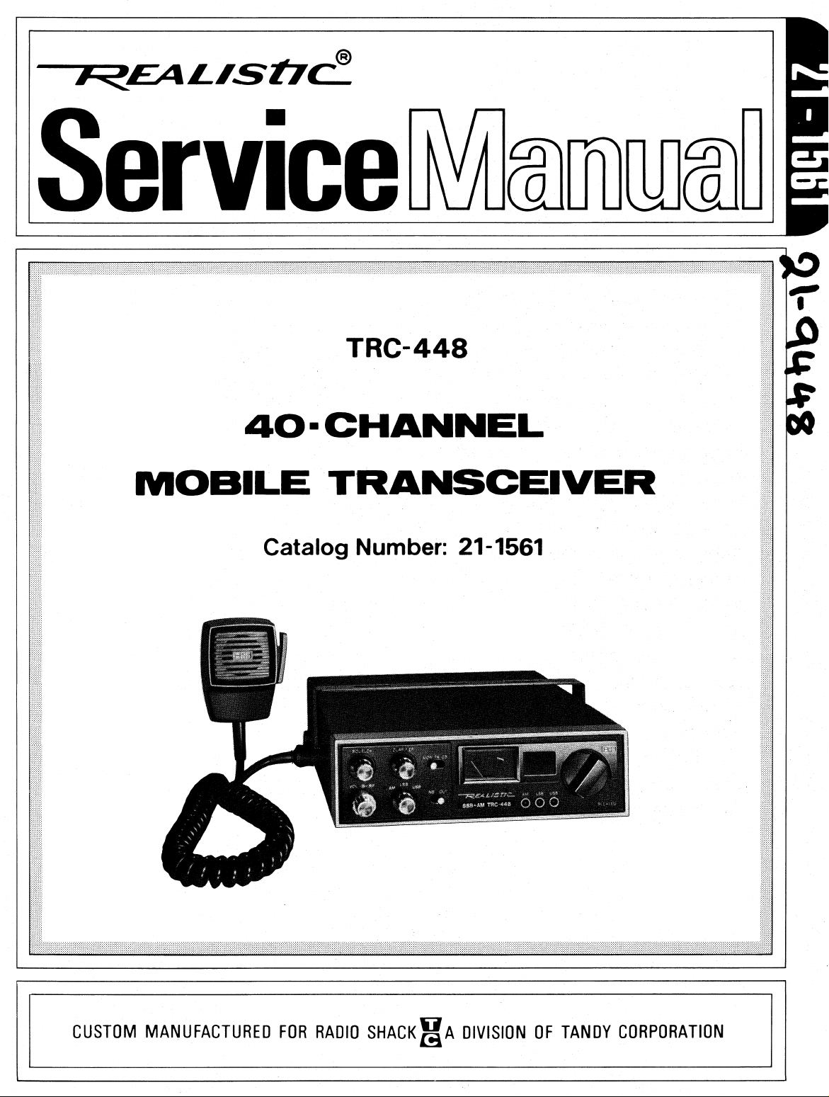
REALISTIC
■
.0
40 - CHANNEL
MOBILE TRANSCEIVER
Catalog Number: 21-1561
00
CUSTOM MANUFACTURED FOR RADIO SHACK A DIVISION OF TANDY CORPORATION
Page 2
CONTENTS
SPECIFICATIONS
BLOCK DIAGRAM
PRINCIPLES OF OPERATION
DISASSEMBLY
ALIGNMENT PREPARATION
ALIGNMENT POSITIONS AND POINTS
PLL SECTION ALIGNMENT CHART
VCO OUTPUT FREQUENCY, IC-2 INPUT FREQUENCY AND CODE TABLE .......
TRANSMITTER SECTION ALIGNMENT CHART
RECEIVER SECTION ALIGNMENT CHART
ALIGNMENT CONNECTIONS
NOISE BLANKER ALIGNMENT CHART
PLL P.C. BOARD TOP VIEW
PLL P.C. BOARD BOTTOM VIEW
MAIN P.C. BOARD TOP VIEW
MAIN P.C. BOARD BOTTOM VIEW
WIRING DIAGRAM (1)
WIRING DIAGRAM (2)
6 - 8
15, 16
3, 4
9
10
11
13
14
18
19
20
21
22
23
5
9
12
17
LED P.C.BOARD (TOP VIEW)
LED P.C.BOARD (BOTTOM VIEW)
LED P.C.BOARD/ CHANNEL SWITCH P.C.BOARD WIRING DIAGRAM
TROUBLESHOOTING
SEMICONDUCTOR VOLTAGE READINGS
PLL P.C.BOARD ASSEMBLY PARTS LIST
MAIN P.C.BOARD ASSEMBLY PARTS LIST
LED P.C.BOARD ASSEMBLY PARTS LIST
CHASSIS ASSEMBLY PARTS LIST
EXPLODED VIEW
SCHEMATIC DIAGRAM
SEMICONDUCTOR LEAD IDENTIFICATION
IC PIN CONFIGURATION
.. . .
24
24
24
25 27
28 33
ti
34
40 49
49
50
51
52, 53
54
54, 55
39
Page 3
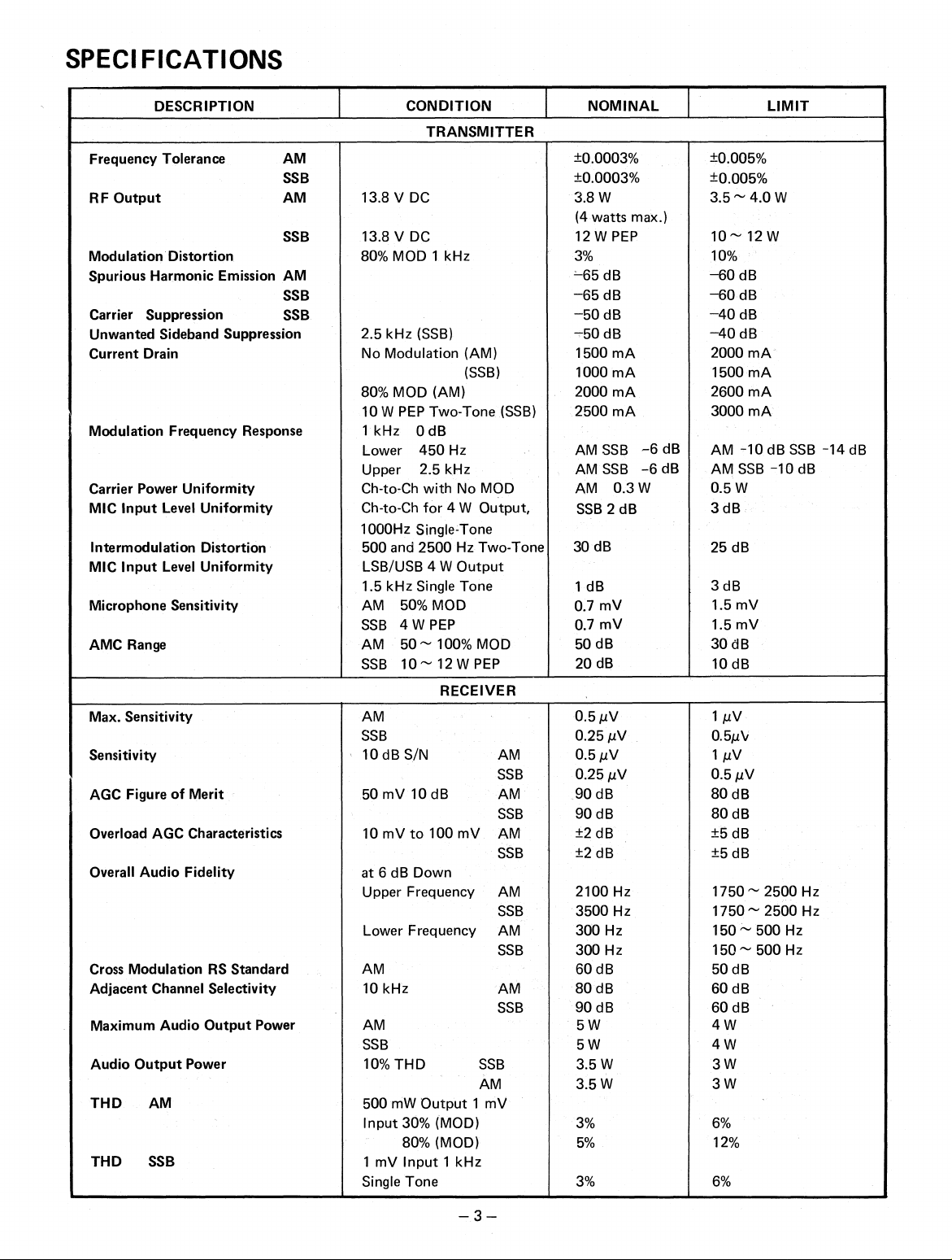
SPECIFICATIONS
DESCRIPTION
Frequency Tolerance
RF Output
Modulation Distortion
Spurious Harmonic Emission AM
Carrier
Unwanted Sideband Suppression
Current Drain
Modulation Frequency Response
Carrier Power Uniformity
MIC Input Level Uniformity
Intermodulation Distortion
MIC Input Level Uniformity
Microphone Sensitivity
AMC Range
Max. Sensitivity
Sensitivity
AGC Figure of Merit
Overload AGC Characteristics
Overall Audio Fidelity
Cross Modulation RS Standard
Adjacent Channel Selectivity
Maximum Audio Output Power
Audio Output Power
THD
THD
Suppression
AM
SSB
AM
SSB
AM
SSB
SSB
SSB
CONDITION
TRANSMITTER
13.8 V DC
13.8 V DC
80% MOD 1 kHz
2.5 kHz (SSB)
No Modulation (AM)
(SSB)
80% MOD (AM)
10 W PEP Two-Tone (SSB)
1 kHz
0 dB
450 Hz
Lower
Upper
Ch-to-Ch with No MOD
Ch-to-Ch for 4 W Output,
1000Hz Single-Tone
500 and 2500 Hz Two-Tone
LSB/USB 4 W Output
1.5 kHz Single Tone
AM 50% MOD
SSB 4 W PEP
AM
SSB
AM
SSB
10 dB S/N
50 mV 10 dB
10 mV to 100 mV AM
at 6 dB Down
Upper Frequency AM
Lower Frequency AM
AM
10 kHz
AM
SSB
10% THD
500 mW Output 1 mV
Input 30% (MOD)
1 mV Input 1 kHz
Single Tone
2.5 kHz
50 - 100% MOD
10 - 12 W PEP
RECEIVER
80% (MOD)
AM
SSB
AM
SSB
SSB
SSB
SSB
AM
SSB
SSB
AM
NOMINAL
±0.0003%
±0.0003%
3.8 W
(4
watts max.)
12 W PEP
3%
-65 dB
65 dB
-
50 dB
-
-50 dB
1500 mA
1000 mA
2000 mA
2500 mA
AM SSB -6 dB
AM SSB -6 dB
0.3 W
AM
SSB 2 dB
30 dB
1 dB
0.7 mV
0.7 mV
50 dB
20 dB
0.5
µV
0.25 µV
0.5 AV
0.25 AV
90 dB
90 dB
±2 dB
±2 dB
2100 Hz
3500 Hz
300 Hz
300 Hz
60 dB
80 dB
90 dB
5 W
5W
3.5 W
3.5W
3%
5%
3%
LIMIT
±0.005%
±0.005%
3.5 - 4.0 W
10 - 12 W
10°/©
-60 dB
-
60 dB
-40 dB
-40 dB
2000 mA
1500 mA
2600 mA
3000 mA
AM -10 dB SSB -14 dB
AM SSB -10 dB
0.5 W
3 dB
25 dB
3 dB
1.5 mV
1.5 mV
30 dB
10 dB
1 AV
0.50
1 AV
0.5 µV
80 dB
80 dB
±5 dB
-
±5 dB
1750 - 2500 Hz
1750'
150 - 500 Hz
150 - 500 Hz
50 dB
60 dB
60 dB
4 W
4W
3 W
3W
6%
12%
6%
2500 Hz
Page 4
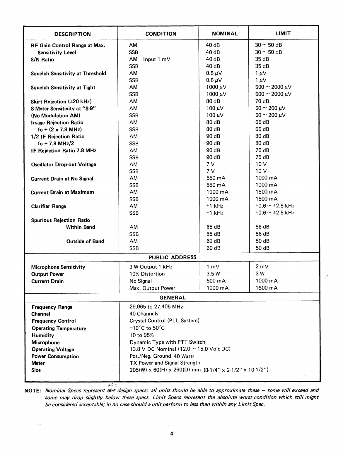
DESCRIPTION
CONDITION
NOMINAL
LIMIT
RF Gain Control Range at Max.
Sensitivity Level
S/N Ratio
Squelch Sensitivity at Threshold
Squelch Sensitivity at Tight
Skirt Rejection (±20 kHz)
5 Meter Sensitivity at "S-9"
(No Modulation AM)
Image Rejection Ratio
fo + (2 x 7.8 MHz)
1/2 IF Rejection Ratio
fo + 7.8 MHz/2
IF Rejection Ratio 7.8 MHz
Oscillator Drop-out Voltage
Current Drain at No Signal
Current Drain at Maximum
Clarifier Range
Spurious Rejection Ratio
Within Band
Outside of Band
Microphone Sensitivity
Output Power
Current Drain
Frequency Range
Channel
Frequency Control
Operating Temperature
Humidity
Microphone
Operating Voltage
Power Consumption
Meter
Size
.
40 dB
40 dB
40 dB
40 dB
0.5 µV
0.5µV
1000 ptV
1000 /../V
80 dB
100µV
100 ptV
80 dB
80 dB
90 dB
90 dB
90 dB
90 dB
7 V
7V
550 mA
550 mA
1000 mA
1000 mA
±1 kHz
±1 kHz
65 dB
65 dB
60 dB
60 dB
1 mV
3.5 W
500 mA
1000 mA
AM
SSB
Input 1 mV
AM
SSB
AM
SSB
AM
SSB
AM
AM
SSB
AM
SSB
AM
SSB
AM
SSB
AM
SSB
AM
SSB
AM
SSB
AM
SSB
AM
SSB
AM
SSB
PUBLIC ADDRESS
3 W Output 1 kHz
10% Distortion
No Signal
Max. Output Power
GENERAL
29.965 to 27.405 MHz
40 Channels
Crystal Control (PLL System)
°
—10
C to 50
°
C
10 to 95%
Dynamic Type with PTT Switch
13.8 V DC Nominal (12.0 — 15.0 Volt DC)
Pos./Neg. Ground 40 Watts
TX Power and Signal Strength
205(W)
x 60(H) x 260(D) mm (8-1/4" x 2-1/2" x 10-1/2")
30 — 50 dB
30 — 50 dB
35 dB
35 dB
1 /./V
1µV
500 — 2000 µV
500 — 2000 µV
70 dB
50 — 200 µV
50 — 200 µV
65 dB
65 dB
80 dB
80 dB
75 dB
75 dB
10 V
V
1 0
1000 mA
1000 mA
1500 mA
1500 mA
±0.6 — ±2.5 kHz
±0.6 — ±2.5 kHz
56 dB
56 dB
50 dB
50 dB
2 mV
3 W
1000 mA
1500 mA
NOTE:
Nominal Specs represent
design specs: all units should be able to approximate these — some will exceed and
&kr
some may drop slightly below these specs. Limit Specs represent the absolute worst condition which still might
be considered acceptable; in no case should a unit perform to less than within any Limit Spec.
Page 5
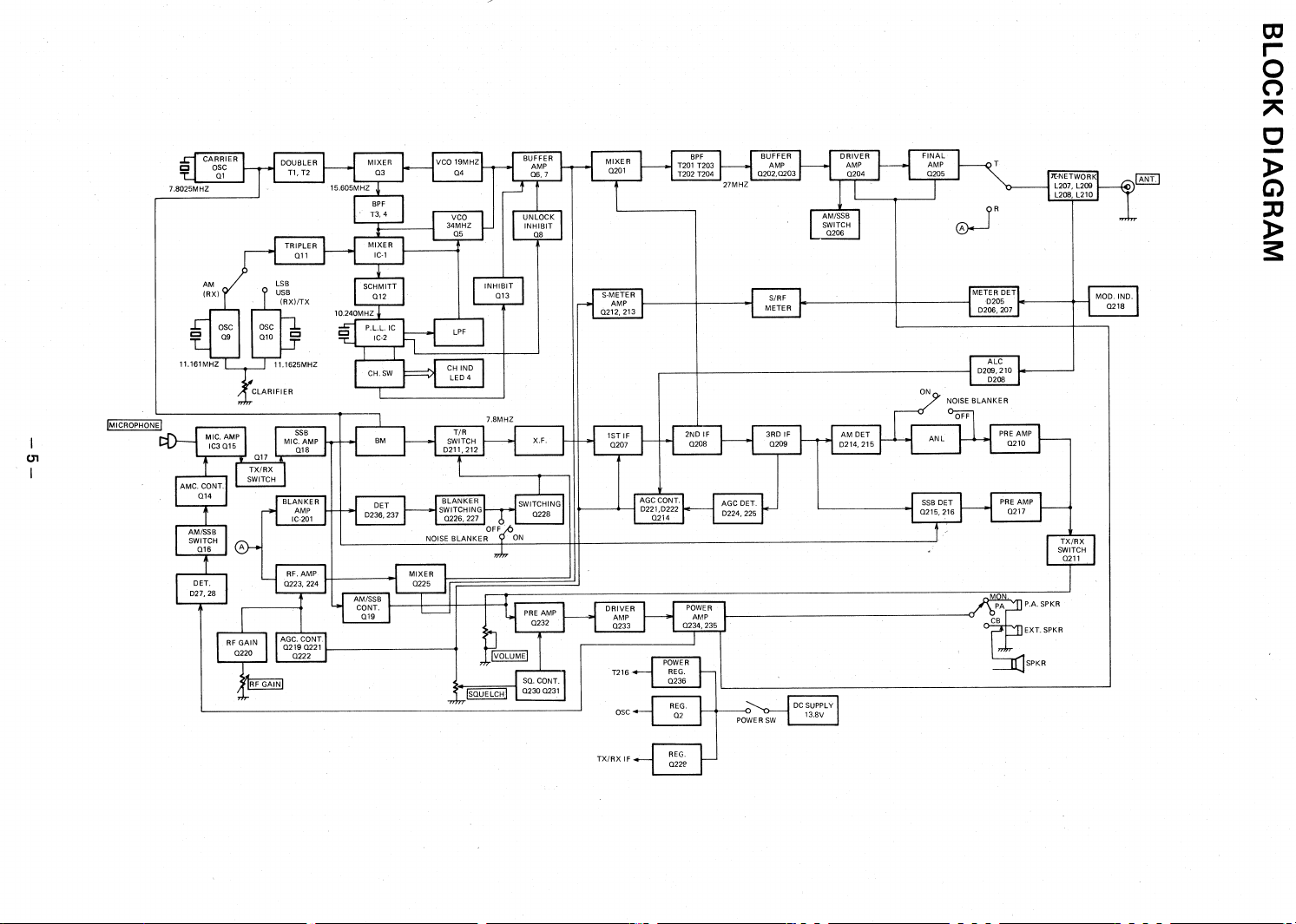
Page 6
PRINCIPLES OF OPERATION
This section of the Service Manual will give you a brief technical description of unique or special circuits
which you might otherwise not understand, notice or be able to troubleshoot
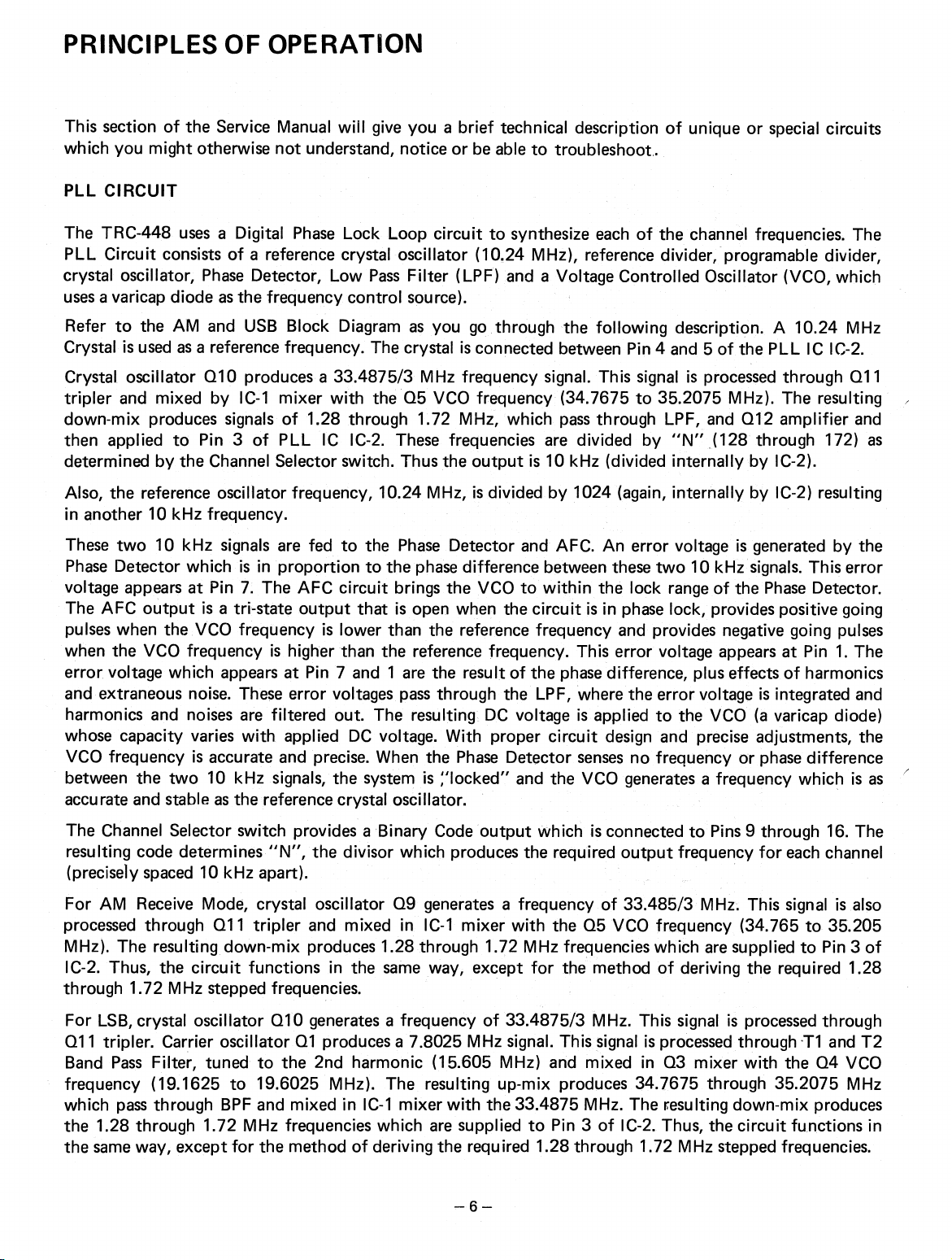
PLL CIRCUIT
The TRC-448 uses a Digital Phase Lock Loop circuit to synthesize each of the channel frequencies. The
PLL Circuit consists of a reference crystal oscillator (10.24 MHz), reference divider, programable divider,
crystal oscillator, Phase Detector, Low Pass Filter (LPF) and a Voltage Controlled Oscillator (VCO, which
uses a varicap diode as the frequency control source).
Refer to the AM and USB Block Diagram as you go through the following description. A 10.24 MHz
Crystal is used as a reference frequency. The crystal is connected between Pin 4 and 5 of the PLL IC IC-2.
Crystal oscillator Q10 produces a 33.4875/3 MHz frequency signal. This signal is processed through Q11
tripler and mixed by IC-1 mixer with the Q5 VCO frequency (34.7675 to 35.2075 MHz). The resulting
down-mix produces signals of 1.28 through 1.72 MHz, which pass through LPF, and Q12 amplifier and
then applied to Pin 3 of PLL IC IC-2. These frequencies are divided by "N" ,(128 through 172) as
determined by the Channel Selector switch. Thus the output is 10 kHz (divided internally by IC-2).
Also, the reference oscillator frequency, 10.24 MHz, is divided by 1024 (again, internally by IC-2) resulting
in another 10 kHz frequency.
,
.
These two 10 kHz signals are fed to the Phase Detector and AFC. An error voltage is generated by the
Phase Detector which is in proportion to the phase difference between these two 10 kHz signals. This error
voltage appears at Pin 7. The AFC circuit brings the VCO to within the lock range of the Phase Detector.
The AFC output is a tri-state output that is open when the circuit is in phase lock, provides positive going
pulses when the VCO frequency is lower than the reference frequency and provides negative going pulses
when the VCO frequency is higher than the reference frequency. This error voltage appears at Pin 1. The
error voltage which appears at Pin 7 and 1 are the result of the phase difference, plus effects of harmonics
and extraneous noise. These error voltages pass through the LPF, where the error voltage is integrated and
harmonics and noises are filtered out. The resulting DC voltage is applied to the VCO (a varicap diode)
whose capacity varies with applied DC voltage. With proper circuit design and precise adjustments, the
VCO frequency is accurate and precise. When the Phase Detector senses no frequency or phase difference
between the two 10 kHz signals, the system is `locked" and the VCO generates a frequency which is as
accurate and stable as the reference crystal oscillator.
The Channel Selector switch provides a Binary Code output which is connected to Pins 9 through 16. The
resulting code determines "NV', the divisor which produces the required output frequency for each channel
(precisely spaced 10 kHz apart).
For AM Receive Mode, crystal oscillator Q9 generates a frequency of 33.485/3 MHz. This signal is also
processed through Oil tripler and mixed in IC-1 mixer with the Q5 VCO frequency (34.765 to 35.205
MHz). The resulting down-mix produces 1.28 through 1.72 MHz frequencies which are supplied to Pin 3 of
IC-2. Thus, the circuit functions in the same way, except for the method of deriving the required 1.28
through 1.72 MHz stepped frequencies.
For LSB, crystal oscillator Q10 generates a frequency of 33.4875/3 MHz. This signal is processed through
Q11 tripler. Carrier oscillator Q1 produces a 7.8025 MHz signal. This signal is processed through Ti and T2
Band Pass Filter, tuned to the 2nd harmonic (15.605 MHz) and mixed in Q3 mixer with the Q4 VCO
frequency (19.1625 to 19.6025 MHz). The resulting up-mix produces 34.7675 through 35.2075 MHz
which pass through BPF and mixed in IC-1 mixer with the 33.4875 MHz. The resulting down-mix produces
the 1.28 through 1.72 MHz frequencies which are supplied to Pin 3 of IC-2. Thus, the circuit functions in
the same way, except for the method of deriving the required 1.28 through 1.72 MHz stepped frequencies.
--6-
Page 7
At Pin 8 of IC-2 a Transmit Inhibit signal is available. It provides a high output (supply voltage to IC-2)
when the synthesizer attains a lock condition, or a low (0 volt) when not in lock. When the output is either
high or low, no phase error pulses are outputted that require detection. This circuit is used to inhibit
transmitter operation if the programmed frequency cannot be properly acquired. The lock detector output
will go low if a frequency error exists for more than 0.5 milliseconds. This signal is applied to the base of
Q8, turning it on or off. Thus the Transmitter can not operate in an unlocked condition of the PLL.
The channel selector switch also has an inhibit function, when the selector switch is set in between two
channel positions, Q13 is turned on to kill Q6.
TX: AM USB
RX : USB
RX : AM
OSC
Q10
OSC Q9
33.485/3 MHz
33.4875/3 MHz
CARRIER
011
TRIPLER
0.5V E
OSC Q1
5V
7.8025 MHz
408
1.5V
BPF
A
10.24 MHz
IC-1
MIXER
4
-
L
IC-2
CI
PLL IC
-
r
5
CHANNEL
SWITCH
AM and USB
(Receive and Transmit)
15.605 MHz
4-1
MIXER
BPF
128-
1.72 MHz
LPF
Q12
AMP
k 9-1
Q3 F
-57775
35.2075 MHz
BPF
34.765 -35.2075 MHz
Q5
VCO
LPF
C16, 07
BUFFER
11.1.1.1.71=
OUTPUT
2V
4
INH BIT
Q8
1, 7
8
19.1625 -19.6025 MHz
Q4
r
VCO
eT
INHIBIT
Q13
Q6, Q7
BUFFER
OUTPUT
2V
TX : LSB
RX : LSB
OSC
Q10
33.4875/3 MHz
Q11
TR IPLER
5V1
BPF
10.24 MHz =
IC-1
MIXER
1.28
1.72 MHz
LPF
Q12
AMP
1, 7
IC-2
-
PLL IC
r
CHANNEL
SWITCH
9--1
8
LSB
(Receive and Transmit)
—7—
LPF
INH BIT
Q8
INHIBIT
Q13
Page 8
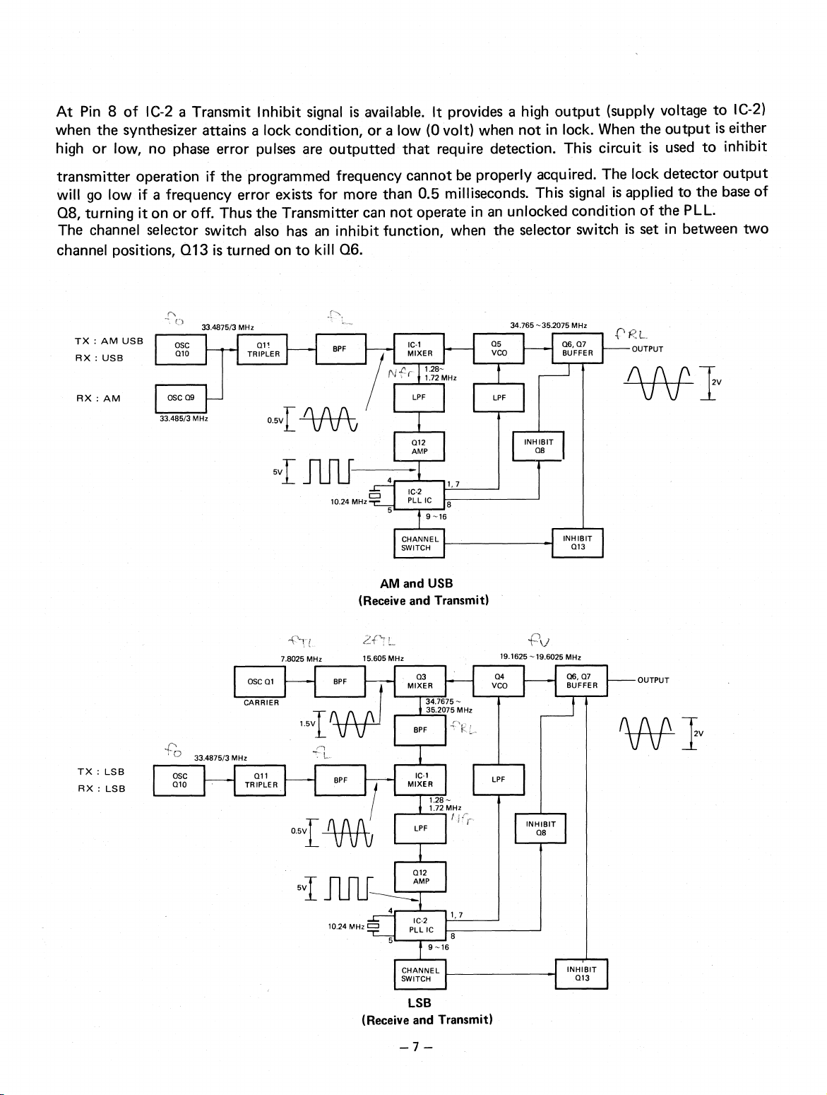
AUTOMATIC MODULATION CONTROL CIRCUIT
The Automatic Modulation Control (AMC) circuit consists of Q14, D26, D27 and D24. The Mic input
signal is fed to pin 4 of the microphone jack and then through R62, C84 to the input terminal (pin 5) of
1C-3 where it is amplified and delivered through C90 and VR4 for further amplification by Q15, Q232,
Q233, Q234 and Q235. The Audio amplifier/Modulation amplifier drives T216, whose secondary incorporates C104, through D228 and R280, which couples a portion of the signal to AMC detector diodes
D27 and D28. D26 (an 8-volt zener) is connected to the output of D27/28; when the detected DC voltage
from D27/28 exceeds 8 volts, D26 conducts. This applies a DC voltage to the base of Q14, thus decreasing
its collector impedance. Notice that the combination of Q14 and VR4 automatically sets the desired audio
signal level processed by the audio amplifier circuitry. VR5 is adjusted to seta modulation level of less than
100%.
VR4 is adjusted to set a modulation level in the SSB mode. IC-3 is a silicon integrated circuit which functions as a audio amplifier with built-in automatic voice-operated gain adjustment. It is designed to provide
an essentially constant output signal for a 60 dB range of input.
.
MIC JACK
AUTOMATIC LIMITER CONTROL (TRANSMITTER)/AUTOMATIC GAIN CONTROL (RECEIVER)
The Automatic Limiter Control (ALC) circuit consists of D209, D210 and Q214. The RF output signal is
detected by 0209 and D210. This applies a negative DC voltage to the gate of Q214, thus decreasing its
source voltage. This source voltage controls Q207's (7.8 MHz amplifier) base bias voltage, thus decreasing
its base voltage. This automatically sets the desired RF output level processed by the RF amplifier circuitry.
V R207 is adjusted to set a RF power level of less than 12 watts PEP.
Q214 is also used as an automatic gain control (AGC). AGC circuit consists of Q214, D221 and D222.
The amplified IF signal is detected by D221, D222, D224, and D225. This voltage is used for fast-attack
AGC. D221, D222 and C279 are used for slow-release AGC. Thus, the circuit functions in the same way,
except for the delivering of source voltage. VR206 is adjusted to set a "0
R62
4
7
4
IC3
C90
V
R4
Q14
Q15
D26
K K
D27
C104 R280
VR5
D28
reading on the S-meter.
-
T216
D228
-11Q207
f
VR206
•
Q214
VR207
C279
—8—
T209
D224
D225
L208
D209
D210
777
Page 9
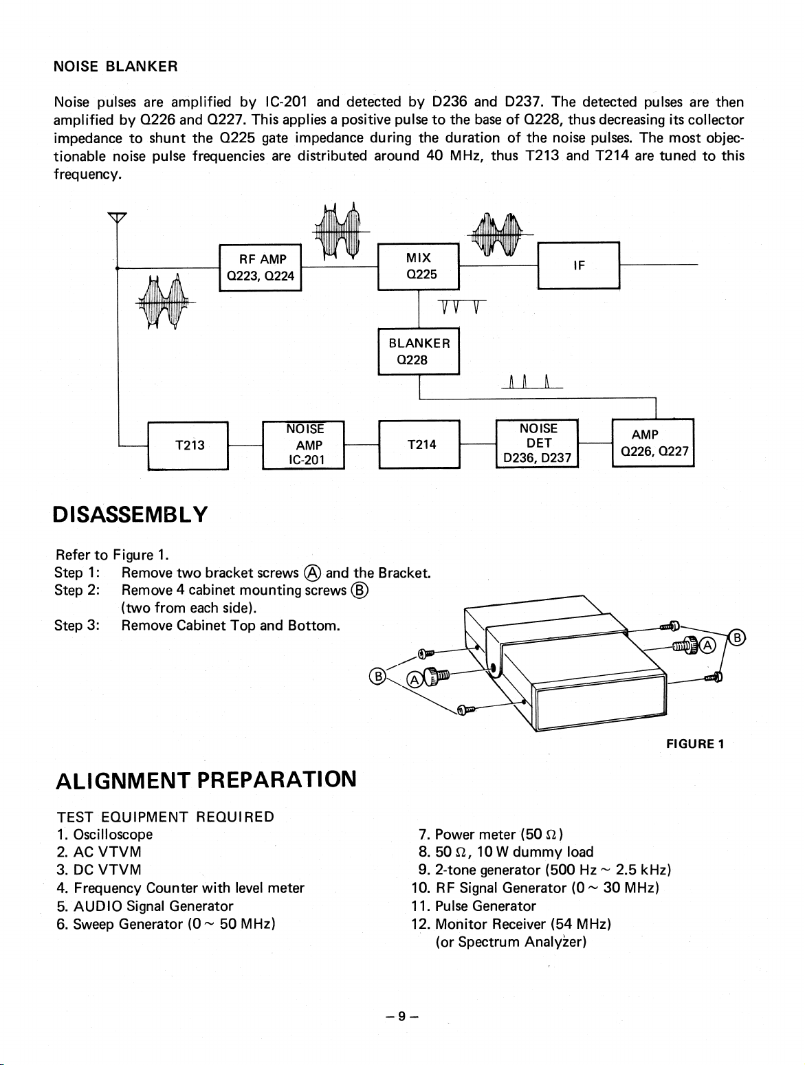
NOISE BLANKER
Noise pulses are amplified by IC-201 and detected by D236 and D237. The detected pulses are then
amplified by Q226 and Q227. This applies a positive pulse to the base of Q228, thus decreasing its collector
impedance to shunt the Q225 gate impedance during the duration of the noise pulses. The most objectionable noise pulse frequencies are distributed around 40 MHz, thus T213 and T214 are tuned to this
frequency.
RF AMP
Q223, Q224
NOISE
T213
AMP
IC-201
DISASSEMBLY
Refer to Figure 1.
Step 1: Remove two bracket screwsAO and the Bracket.
Step 2: Remove 4 cabinet mounting screws ®
(two from each side).
Step 3: Remove Cabinet Top and Bottom.
MIX
Q225
VV V
BLANKER
Q228
T214
nn
N
NOISE
DET
D236, D237
IF
AMP
Q226, Q227
ALIGNMENT PREPARATION
TEST EQUIPMENT REQUIRED
Oscilloscope
1.
AC VTVM
2.
DC VTVM
3.
4.
Frequency Counter with level meter
AUDIO Signal Generator
5.
Sweep Generator (0 50 MHz)
6.
7.
Power meter (50
8.
50
2, 10
9.
2-tone generator (500 Hz — 2.5 kHz)
10.
RF Signal Generator (0 30 MHz)
Pulse Generator
11.
12.
Monitor Receiver (54 MHz)
(or Spectrum Analyier)
W dummy load
2)
FIGURE 1
Page 10
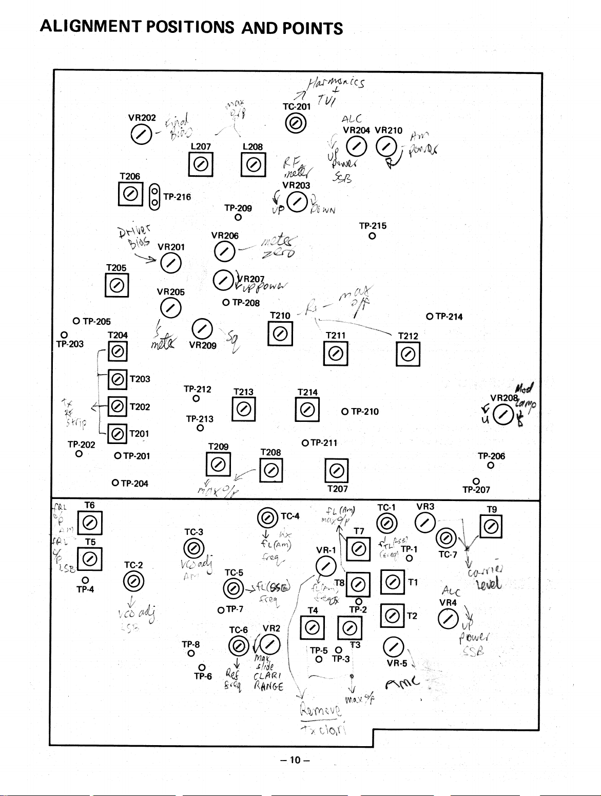
ALIGNMENT POSITIONS AND POINTS
Page 11
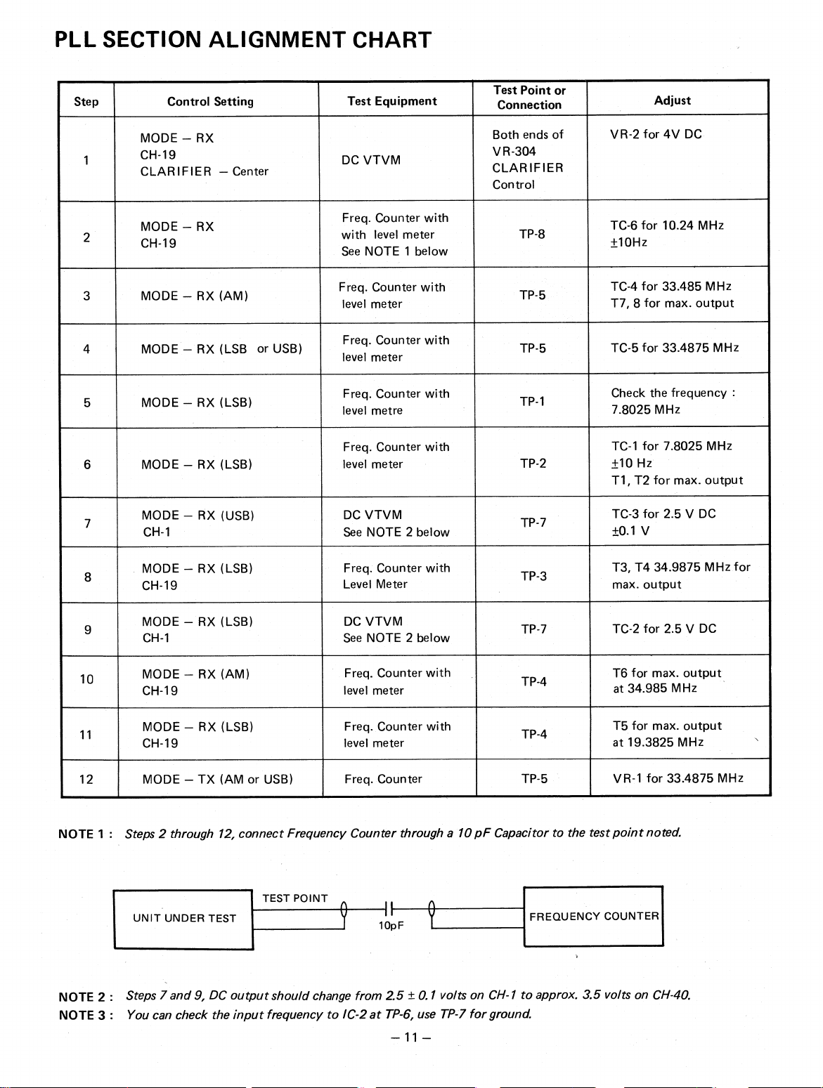
PLL SECTION ALIGNMENT CHART
Step
1
2
3
4
5
6
Control Setting
MODE — RX
CH-19
CLARIFIER — Center
MODE — RX
CH-19
MODE — RX (AM)
MODE — RX (LSB or USB)
MODE — RX (LSB)
MODE — RX (LSB)
Test Equipment
DC VTVM
Freq. Counter with
with level meter
See NOTE 1 below
Freq. Counter with
level meter
Freq. Counter with
level meter
Freq. Counter with
level metre
Freq. Counter with
level meter
Test Point or
Connection
Both ends of
VR-304
CLARIFIER
Control
TP-8
TP-5
TP-5
TP-1
TP-2
Adjust
VR -2 for 4V DC
TC-6 for 10.24 MHz
+10Hz
TC-4 for 33.485 MHz
T7, 8 for max. output
TC-5 for 33.4875 MHz
Check the frequency :
7.8025 MHz
TC-1 for 7.8025 MHz
+10 Hz
T1, T2 for max. output
7
8
9
10
11
12
NOTE 1 :
MODE — RX (USB)
CH-1
MODE — RX (LSB)
CH-19
MODE — RX (LSB)
CH-1
MODE — RX (AM)
CH-19
MODE — RX (LSB)
CH-19
MODE — TX (AM or USB)
Steps 2 through 12, connect Frequency Counter through a 10 pF Capacitor to the test point noted.
TEST POINT
UNIT UNDER TEST
DC VTVM
See NOTE 2 below
Freq. Counter with
Level Meter
DC VTVM
See NOTE 2 below
Freq. Counter with
level meter
Freq. Counter with
level meter
Freq. Counter
I 1
10pF
TP-7
TP-3
TP-7
TP-4
TP-4
TP-5
FREQUENCY COUNTER
TC-3 for 2.5 V DC
±0.1 V
T3, T4 34.9875 MHz for
max. output
TC-2 for 2.5 V DC
T6 for max. output
at 34.985 MHz
T5 for max. output
at 19.3825 MHz
VR-1 for 33.4875 MHz
NOTE 2 :
NOTE 3 :
Steps 7 and 9, DC output should change from 2.5 ± 0.1 volts on CH-1 to approx. 3.5 volts on CH-40.
You can check the input frequency to IC-2 at TP-6, use TP-7 for ground.
—11
—
Page 12

ITX
Frequency (MHz)
CH
1
2
3
4
5
6
7
8
9
10
11
12
13
14
15
16
17
18
19
20
21
22
23
,
24
25
26
27
28
29
-
30
31
32
33
34
35
36
37
38
39
40
26.965
26.975
26.985
27.005
27.015
27.025
27.035
27.055
27.065
27.075
27.085
27.105
27.115
27.125
27.135
27.155
27.165
27.175
27.185
27.205
27.215
27.225
27.255
27.235
27.245
27.265
27.275
27.285
27.295
27.305
27.315
27.325
27.335
27.345
27.355
27.365
27.375
27.385
27.395
27.405
RX (AM) +1.5 kHz
34.765
34.775
34.785
34.805
34.815
34.825
34.835
34.855
34.865
34.875
34.885
•
34.905
34.915
34.925
34.935
34.955
34.965
34.975
34.985
35.005
35.015
35.025
35.055
35.035
35.045
35.065
35.075
35.085
35.095
35.105
35.115
35.125
35.135
35.145
35.155
35.165
35.175
35.185
35.195
35.205
VCO
(LSB)
RX (LSB)
19.1625
19.1725
19.1825
19.2025
19.2125
19.2225
19.2325
19.2525
19.2625
19.2725
19.2825
19.3025
19.3125
19.3225
19.3325
19.3525
19.3625
19.3725
19.3825
19.4025
19.4135
19.4225
19.4525
19.4325
19.4425
19.4625
19.4725
19.4825
19.4925
19.5025
19.5125
19.5225
19.5325
19.5425
19.5525
19.5625
19.5725
19.5825
19.5925
19.6025
1.5 kHz
+
TX (AM USB)
RX (USB)
+
34.7675
34.7775
34.7875
34.8075
34.8175
34.8275
34.8375
34.8575
34.8675
34.8775
34.8875
34.9075
34.9175
34.9275
34.9375
34.9575
34.9675
34.9775
34.9875
35.0075
35.0175
35.0275
35.0575
35.0375
35.0475
35.0675
35.0775
35.0875
35.0975
35.1075
35.1175
35.1275
35.1375
35.1475
35.1575
19.1675
35.1775
35.1875
35.1975
35.2075
1.5 kHz
fin
(MHz)
1.28
1.29
1.30
1.32
1.33
1.34
1.35
1.37
1.38
1.39
1.40
1.42
1.43
1.44
1.45
1.47
1.48
1.49
1.50
1.52
1.53
1.54
1.57
1.55
1.56
1.58
1.59
1.60
1.61
1.62
1.63
1.64
1.65
1.66
1.67
1.68
1.69
1.70
1.71
1.72
N
128
129
130
132
133
134
135
137
138
139
140
142
143
144
145
147
148
149
150
152
153
154
157
155
156
158
159
160
161
162
163
164
165
166
167
168
169
170
171
172
INPUT CODE
PIN NO.
15
0
0
1
0
0
1
1
0
1
1
0
1
1
0
0
1
0
0
0
0
1
0
1
0
1
1
0
0
1
1
0
0
1
1
0
0
1
1 1
0
16
0
1
0
0
1
0
1
1
0
1
0
0
1
0
1
1
0
1
0
0
1
0
0
0
0
0
0
0
0
1
1
/1A
1
103
1
1
1
1
1
0
0
1
3N3
A
14
0
0
0
0
0
0
0
0
0
0
0
0
0
1
1
1
1
1
1
1
1
1
1
1
1
1
1
0
0
0
0
.0
0
0
0
0
0
0
0
0
13
0
0
0
0
0
0
0
1
1
1
1
1
1
0 0
0
0
0
0
0
1
1
1
1
1
1
1
1
0
0
0
0
0
0
0
0
1
1
1
1
1
0
0
0
1
1
1
1
0
0
0
1
1
1
0
0
1
1
1 1
0
0
0
1
0
1
1
1
0
0
0
0
1
1
1
1
0
0
0
0
1
11 12
10
9
0
0
1
0
0
1
0 0
1
0 0
1
0
0
1
0
0
1
1
0
0
1
1
1
1
1
1
1
1
1
1
1
1
1
1
1
1
1
1
1
1
1
1
1
1
1
1
1
1
1
1
1
1
1
0
0
0
0
0
0
0
0
0
0
0
0
0
0
0
0
0
0
0
0
0
0
0
0
0
0
0
0
0
0
0
0
0
0
0
0
0
0
0
0
1
0
1
0
1
0
1
0
1
0
1
0
1
0
1
0
1
0
1
0
1
0
1
0
0
1
Page 13
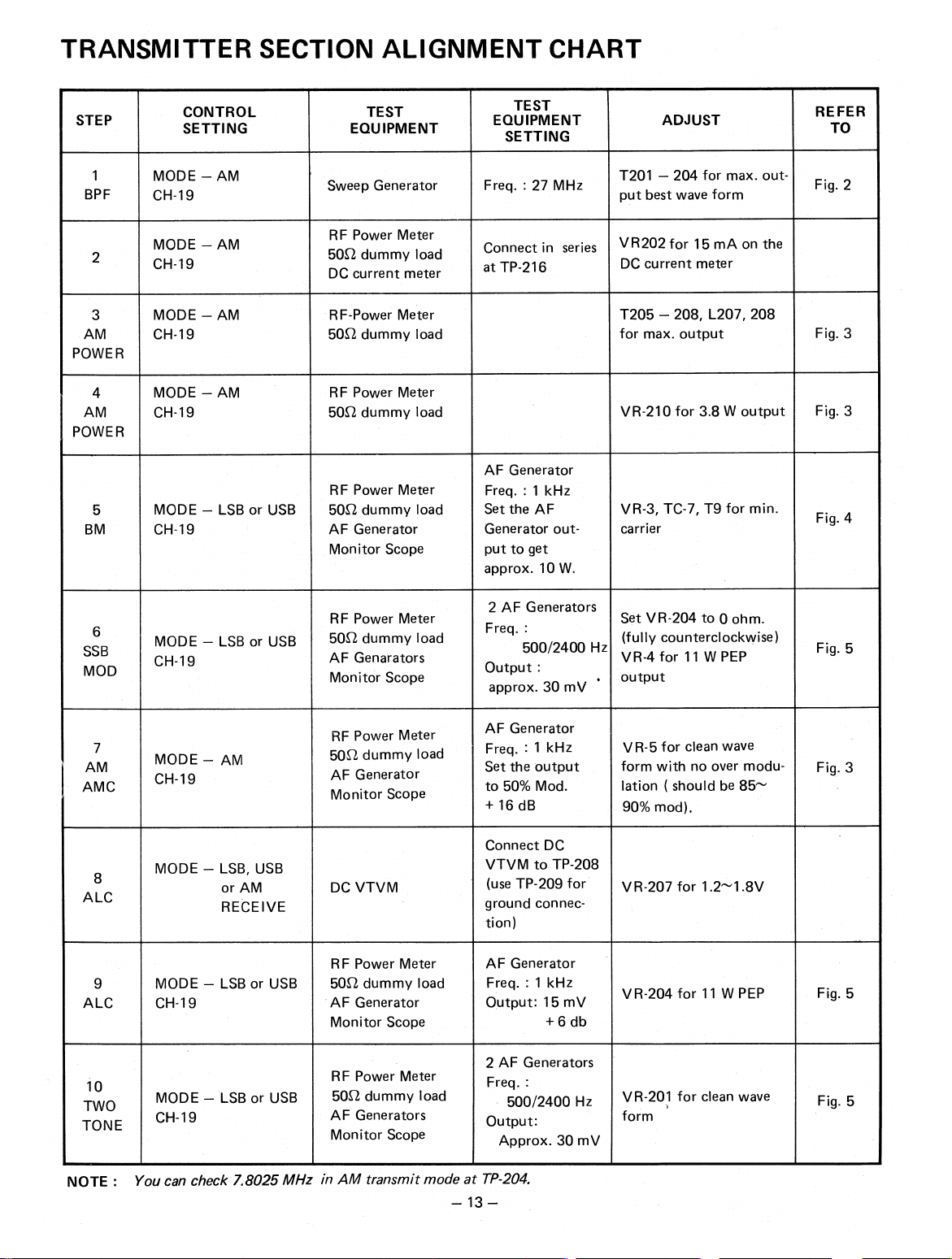
TRANSMITTER SECTION ALIGNMENT CHART
STEP
1
BPF
2
3
AM
POWER
4
AM
POWER
5
BM
CONTROL
SETTING
MODE — AM
CH-19
MODE — AM
CH-19
MODE — AM
CH-19
MODE — AM
CH-19
MODE — LSB or USB
CH-19
TEST
EQUIPMENT
Sweep Generator
RF Power Meter
502 dummy load
DC current meter
RF-Power Meter
502 dummy load
RF Power Meter
502 dummy load
RF Power Meter
502 dummy load
AF Generator
Monitor Scope
TEST
EQUIPMENT
SETTING
Freq. : 27 MHz
Connect in series
at TP-216
AF Generator
Freq. : 1 kHz
Set the AF
Generator output to get
approx. 10 W.
ADJUST
T201 — 204 for max. output best wave form
VR202 for 15 mA on the
current meter
DC
T205 — 208, L207, 208
for max. output
VR-210 for 3.8 W output
VR-3, TC-7, T9 for min.
carrier
REFER
TO
Fig. 2
Fig. 3
Fig. 3
Fig. 4
6
SSB
MOD
7
AM
AMC
8
ALC
9
ALC
10
TWO
TONE
MODE — LSB or USB
CH-19
MODE — AM
CH-19
MODE — LSB, USB
or AM
RECEIVE
MODE — LSB or USB
CH-19
MODE — LSB or USB
CH-19
RF Power Meter
5
2 dummy load
50
AF Genarators
Monitor Scope
RF Power Meter
502 dummy load
AF Generator
Monitor Scope
DC VTVM
RF Power Meter
502 dummy load
AF Generator
Monitor Scope
RF Power Meter
502 dummy load
AF Generators
Monitor Scope
2 AF Generators
Freq. :
500/2400 Hz
Output :
approx. 30 mV
AF Generator
Freq. : 1 kHz
Set the output
to 50% Mod.
+ 16 dB
Connect DC
VTVM to TP-208
(use TP-209 for
ground connection)
AF Generator
Freq. : 1 kHz
Output: 15 mV
+ 6 db
2 AF Generators
Freq.
500/2400 Hz
Output:
Approx. 30 mV
Set VR-204 to 0 ohm.
(fully counterclockwise)
VR-4 for 11 W PEP
.
output
VR-5 for clean wave
form with no over modulation ( should be 85—
90% mod).
VR-207 for 1.2-1.8V
VR-204 for 11 W PEP
VR-201 for clean wave
form
Fig. 5
Fig. 3
Fig. 5
Fig. 5
NOTE :
You can check 7.8025 MHz
in
AM
transmit mode at
—13
TP-204.
Page 14
STEP
CONTROL
SETTING
_
TEST
EQUIPMENT
TEST
EQUIPMENT
SETTING
,
ADJUST
REFER
TO
11
RF
METER
12
MOD
IND
.
13
HAFT-
MON ICS
MODE — AM
CH-19
MODE — AM
CH-19
MODE — AM
CH-19
RF Power Meter
502 dummy load
RF Power Meter
502 dummy load
AF Generator
Monitor Scope
RF Power Meter
502 dummy load
54 MHz Monitor
Receiver
(or Spectrum Analyzer if available)
AF Generator
Freq. `. 1 kHz
Set the AF
Generator output to get 30%
mod.
.
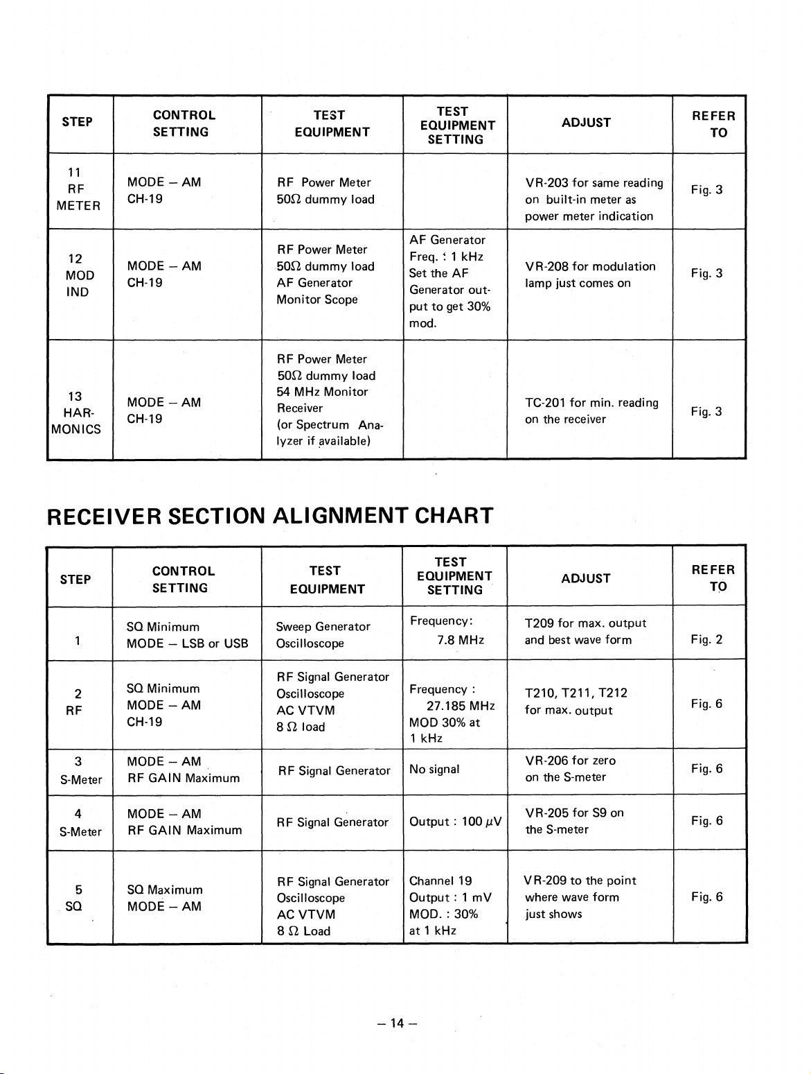
RECEIVER SECTION ALIGNMENT CHART
TEST
EQUIPMENT
SETTING
STEP
CONTROL
SETTING
TEST
EQUIPMENT
VR-203 for same reading
on built-in meter as
power meter indication
VR-208 for modulation
lamp just comes on
.
TC-201 for min. reading
on the receiver
ADJUST
Fig 3
Fig. 3
Fig. 3
REFER
TO
1
2
RF
3
S-Meter
4
S-Meter
5
SQ
SQ Minimum
MODE — LSB or USB
SQ Minimum
MODE — AM
CH-19
MODE — AM
RF GAIN Maximum
MODE — AM
RF GAIN Maximum
SQ Maximum
MODE — AM
Sweep Generator
Oscilloscope
RF Signal Generator
Oscilloscope
AC VTVM
8 2 load
RF Signal Generator
RF Signal Generator
RF Signal Generator
Oscilloscope
AC VTVM
8 2 Load
Frequency:
7.8 MHz
Frequency :
27.185 MHz
MOD 30% at
1 kHz
No signal
Output : 100 µV
Channel 19
Output : 1 mV
MOD. : 30%
at 1 kHz
T209 for max. output
and best wave form
T210, T211, T212
for max. output
VR-206
on the S-meter
VR-205 for S9 on
the S-meter
VR-209 to the point
where wave form
just shows
for zero
Fig. 2
Fig. 6
Fig. 6
Fig. 6
Fig. 6
Page 15

ALIGNMENT CONNECTIONS
BAND PASS FILTER ALIGNMENT
Connect the instruments as shown in Figure 2.
Best wave form
FIGURE 2
Mode Switch
AM
USB or LSB
Input Test Point
hot
TP-201
TP-206
or TP-214
ground
TP-202
TP-207
or TP-215
TRANSMITTING SECTION ALIGNMENT
Connect the instruments as shown in Figure 3.
Output Test Point
hot
TP-205
TP-212
ground
TP-203
TP-213
MONITOR SCOPE WAVE FORM
Sweep Generator
27 MHz
7.8 MHz
FIGURE 3
— 15 —
Page 16

BALANCED MODULATOR ALIGNMENT
Connect the instruments as shown in Figure 4.
MIC Jack
Pin 4
AF GENERATOR
UNIT
UNDER TEST
ANT. Jack
1
FIGURE 4
50S1 Load
SPECTRUM
ANALYZE R
or
OSCILLOSCOPE
Step
1
2
3
4
Control
Setting
SSB TX
SSB TX
SSB TX
SSB TX
Adjust
AF Generator
VR-3
T-9
TC-7
TRANSMITTING SECTION ALIGNMENT (SSB)
Connect the instrument as shown is Figure 5.
AF
GENERATOR
2 Tone SW
ON/OFF
AF
GENERATOR
MIC Jack
Pin 4
0
/
UNIT
UNDER
TEST
13.8 V
DC POWER
SUPPLY
ANT. Jack
5on
Load
POWER
METER
MONITOR
SCOPE
SPECTRUM
ANALYZER
(if available)
Remarks
To get 10W output power
Note the carrier level at 10W
output power
Remove AF Generator
Minimum carrier level
Minimum carrier level
Repeat steps 2 and 3
*AF input frequency
2500 Hz
*AF Two-tone input frequency
Select frequencies not related harmonically.
The test tones of 500 Hz and 2400 Hz are suggested.
*Idling current of Final Transistor : Approx. 50 mA
FIGURE 5
RECEIVER SECTION ALIGNMENT
Connect the instruments as shown in Figure 6.
RF SIGNAL
GENERATOR
ANT Jack
UNIT
UNDER TEST
TRC-448
13.8 V
DC POWER
SUPPLY
— 16 —
VTVM
82 Load
SPKR Jack
OSCILLOSCOPE
FIGURE 6
Page 17

NOISE BLANKER ALIGNMENT CHART
Without pulse generator
SIGNAL GENERATOR
Control Setting
Channel -19
UNIT UNDER TEST
Adjust
T213
T214
D237
TP-210
D236
1N60
TP-211
Tune T213 and T214 for maximum
reading on the. DC VTVM
Ant. Jack
T214 0.01 (M) 1N60
Test Equipment
Signal Generator 40MHz
(Output :10µV)
Connect Oscilloscope
DC VTVM
0 0
DC VTVM
Procedure
With pulse generator
SIGNAL GENERATOR
PULSE GENERATOR
Control Setting
CH : 19
(27.185 MHz)
T PAD
Ant. Jack
Test Equipment
Signal Generator
(Output : 1 µV)
Pulse Generator
(Pulse width : 1 µSec.)
: 10 mSec.)
(Cycle
: 1V P.P.)
(Output
Connect Oscilloscope
UNIT UNDER TEST
Adjust
T214
OSCILLOSCOPE
0 0
Audio Out
Procedure
Tune T214 for Max. S/N ratio
on the oscilloscope
Page 18

PLL P C.BOARD (TOP VIEW)
TP- 2
;11:11111111111111'
:1
,,,
TP-7
TP-3
I
I TP-4,
- 18 -
Page 19
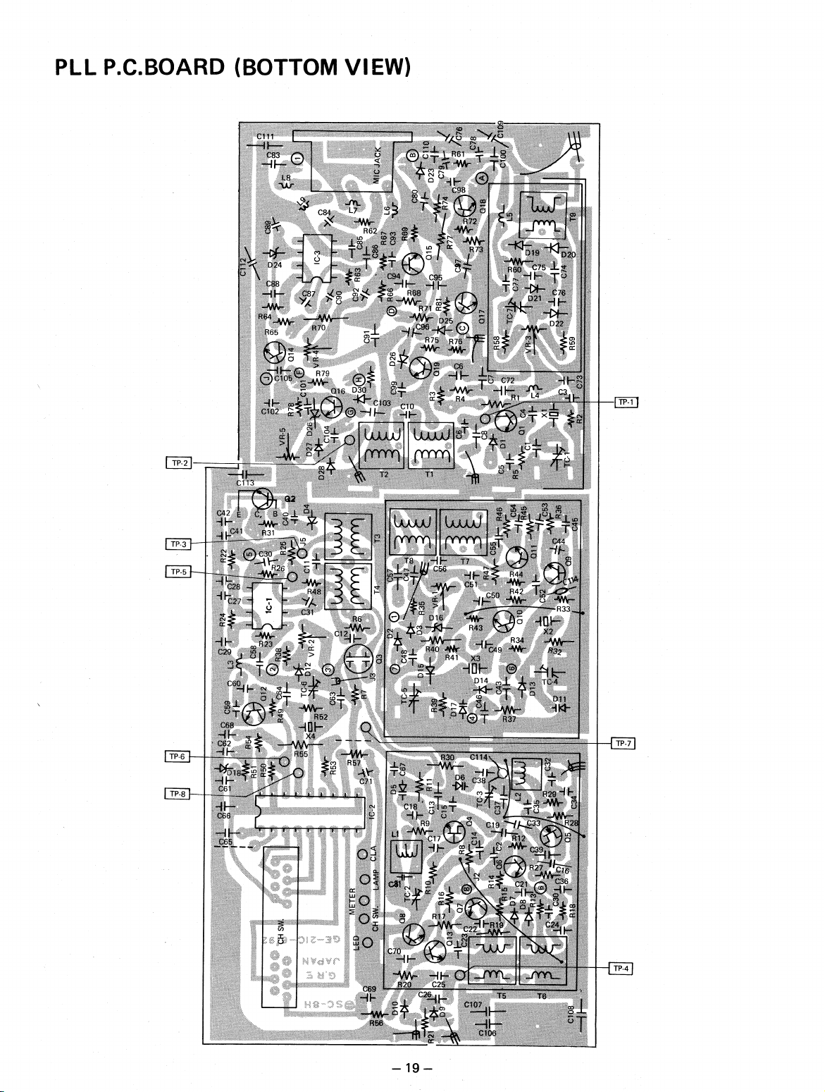
PLL P.C.BOARD (BOTTOM VIEW
Page 20

MAIN P.C.BOARD (TOP VIEW)
1TP-214(
r 023
/el k
ITP-2061
ITP-2071
TP-215
TP-209
1TP-2081
1TP-2161
}TP-2111
ITP-2011
TP-204
1TP-205
1TP-2031
TP-2021
Page 21

MAIN P.C.BOARD (BOTTOM VIEW)
P-206
•
ITP-210I
P-213
"IFFR-T1
3
ITP-2161
TTP-202'
ITP-2031
1TP-2051
- 21 -
Page 22

WIRING DIAGRAM (1)
RF GAIN VOL
IPASPKR
J
EXT SPKR
- 22 -
Page 23

WIRING DIAGRAM (2)
ORG
RED
1=
NOISE BLANKER SW I
BLU
0
L1J
CC
[CI
DC 13.8V
C237
GI
- 23 -
Page 24

LED P.C.BOARD
(TOP VIEW)
USB
(BOTTOM VIEW)
•
LED P.C.BOARD/ CHANNEL SWITCH P.C.BOARD WIRING
DIAGRAM
ORG
RED!
BRN
YEL
USB
BLK
BLK
BRN
RED
ORG
YEL
GRN
BLU
VIO
WHT
•
- 24 --
Page 25
TROUBLE SHOOTING
Before starting trouble shooting, first check the PLL section with the channel selector set at CH-19.
STEP
If above 2 steps are
PLL SECTION
1)
Wrong frequency in step 1 above
2)
Wrong frequency in step 2 above
CONTROL
SETTING
1
2
OK, the PLL section is OK.
.
RX (AM)
RX (LSB) or
TX (LSB)
Symptom
TEST
POINT
TP-4
TP-4
TEST
EQUIPMENT
Freq. Counter
Freq. Counter
Defective Q5, D6, L2, Q9, X2, Q11, IC-1 and/or associated
circuit components
Defective Q4, D5, L1, Q1, Ti, T2, Q10, X3, Q11 and/or
associated circuit components
OUTPUT
34.985 MHz
19.3825 MHz
Possible Cause
REMARKS
VCO freq.
VCO freq.
3)
Wrong frequency in both steps 1 and 2 above
OTHER SECTIONS
1)
Meter lamp does not light and/or set fails
to operate when power is on
2)
Fuse blows
3)
Does not receive AM
RX SSB : OK
TX AM SSB : OK
Symptom
Defective IC-2, X4, Q3, Q4, Q6, Q7, Q8, Q13 and/or
channel selector switch
Possible Cause
A)
Faulty DC power cord
B)
Defective Q229 and/or associated circuit components
Defective power cord
C)
D)
Defective meter lamp
E) Fuse blown
A)
Collector of the Q204, Q205, Q234 and/or Q235 are
shorted to chassis.
B)
Reverse polarity
C)
Defective Q204, Q205, Q234, Q235 and/or D204
D)
Defective Q299 and/or D244
A)
Defective D214, D215 and/or associated circuit
components
B)
Defective Q210 and/or associated circuit componets
C)
Defective Q211, D255 and/or associated circuit
components
— 25 —
Page 26

Symptom
4)
Does not receive SSB
RX AM : OK
TX AM SSB : OK
5)
Does not receive or transmit SSB
RX AM : OK
TX AM : OK
6)
Does not receive AM/SSB or transmit SSB
TX AM : OK
Possible Cause
A)
Defective Q215, Q216 and/or associated circuit
components
B)
Defective Q217 and/or associated circuit components
A) Defective Q1 and/or associated circuit components
A) Defective XF201, Q207, Q208, T207, T208 and/or
associated circuit components
7)
Does not receive both AM and SSB
8)
No sound
TX AM SSB : OK
9)
Does not transmit AM and SSB
10)
Does not transmit AM
TX SSB : OK
11)
Does not transmit SSB
TX AM : OK
RX AM SSB : OK
12)
SQUELCH Control does not function
A) Defective Q223, Q224, Q235 and/or associated circuit
components
Defective speaker or defective EXT. SPKR jack
A)
B)
Faulty Squelch control circuit
Defective Relay
C)
A)
Defective Q201, Q202, Q203, Q204, Q205 and/or
associated circuit components
Defective Relay, D251 and/or Microphone PTT switch
B)
C)
Defective MODE Switch
A) Defective Q236, D228, MODE switch and/or associated
circuit components
A)
Defective IC-3, Q15, Q17, Q18 and/or associated circuit
components
B)
Defective D19, D20, D21, D22, T9, D211 and/or
associated circuit components
Defective D249, D250 and/or associated circuit
C)
components
A)
Defective VR-209 and/or VR-303
B)
Defective VR-206
Defective Q230, Q231 and/or associated circuit
C)
components
13)
Receiver oscillates on AM
RX SSB : OK
14)
Low sensitivity
TX SSB : OK
15)
No modulation on AM
TX SSB : OK
RX AM : OK
A)
Defective D1
B)
Defective MODE switch
A)
Faulty AGC circuit Q219, Q220, Q221 and/or associated
circuit components
B)
Defective Q228 and/or associated circuit components
Defective Q223, Q224, Q225 and/or associated circuit
C)
components
A)
Defective IC-3, Q15, Q17, Q18 and/or associated circuit
components
B)
Defective T216
— 26 --
Page 27
Symptom
Modulation indicator does not flash on AM.
16)
MOD : OK
Possible Cause
Defective Q218, D226, D227 and/or associated circuit
A)
components
Defective modulation indicator lamp
B)
Meter lamp does not turn on in RX.
17)
Meter lamp does not turn on in MON/PA
18)
RX AGC and SSB TX ALC does not work
19)
Noise blanker and ANL does not work.
20)
PA does not work.
21)
CB : OK
RF control does not work.
22)
CLARIFIER does not work.
23)
A) Defective D229
A) Defective D230
A) Defective Q214 and/or associated circuit components
Defective IC-201, Q226, Q228,D236. D237, D238,
A)
D239 and/or associated circuit components
Defective D216 and/or associated circuit components
B)
Defective NB switch
C)
Defective PA—CB switch
A)
Defective PA jack
B)
A) Defective Q220, D253 and/or associated circuit
components
Defective D12,D13, D14 and/or associated circuit
A)
components
Defective VR-304 and/or VR-2
B)
I
Page 28
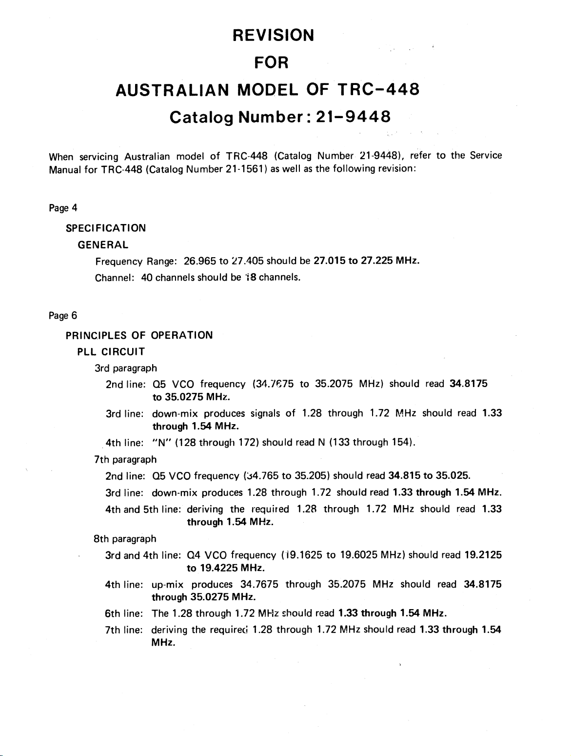
REVISION
FOR
AUSTRALIAN MODEL OF TRC-448
Catalog Number: 21-9448
When servicing Australian model of TRC-448 (Catalog Number 21-9448), refer to the Service
Manual for TRC-448 (Catalog Number 21-1561) as well as the following revision:
Page 4
SPECI FICATION
GENERAL
Frequency Range: 26.965 to 27.405 should be 27.015 to 27.225 MHz.
Channel: 40 channels should be 18 channels.
Page 6
PRINCIPLES OF OPERATION
PLL CIRCUIT
3rd paragraph
2nd line: Q5 VCO frequency (34.7F;75 to 35.2075 MHz) should read 34.8175
to 35.0275 MHz.
3rd line: down-mix produces signals of 1.28 through 1.72 MHz should read 1.33
through 1.54 MHz.
4th line: "N" (128 through 172) should read N (133 through 154).
7th paragraph
2nd line: Q5 VCO frequency (;54.765 to 35.205) should read 34.815 to 35.025.
3rd line: down-mix produces 1.28 through 1.72 should read 1.33 through 1.54 MHz.
4th and 5th line: deriving the required 1.28 through 1.72 MHz should read 1.33
through 1.54 MHz.
8th paragraph
3rd and 4th line: Q4 VCO frequency (19.1625 to 19.6025 MHz) should read 19.2125
to 19.4225 MHz.
4th line: up-mix produces 34.7675 through 35.2075 MHz should read 34.8175
through 35.0275 MHz.
6th line: The 1.28 through 1.72 MHz should read 1.33 through 1.54 MHz.
7th line: deriving the required 1.28 through 1.72 MHz should read 1.33 through 1.54
MHz.
Page 29
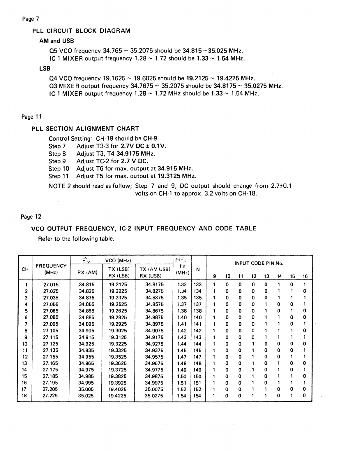
Page 7
PLL CIRCUIT BLOCK DIAGRAM
AM and USB
Q5 VCO frequency 34.765 - 35.2075 should be 34.815 -35.025 MHz.
IC-1 MIXER output frequency 1.28 - 1.72 should be 1.33 - 1.54 MHz.
LSB
Q4 VCO frequency 19.1625 - 19.6025 should be 19.2125 - 19.4225 MHz.
Q3 MIXER output frequency 34.7675 - 35.2075 should be 34.8175 - 35.0275 MHz.
IC-1 MIXER output frequency 1.28 - 1.72 MHz should be 1.33 - 1.54 MHz.
Page 11
PLL SECTION ALIGNMENT CHART
Control Setting: CH-19 should be CH-9.
Adjust T3-3 for 2.7V DC ± 0.1V.
Step 7
Step 8 Adjust T3, T4 34.9175 MHz.
Adjust TC-2 for 2.7 V DC.
Step 9
Step 10 Adjust T6 for max. output at 34.915 MHz.
Step 11 Adjust T5 for max. output at 19.3125 MHz.
NOTE 2 should read as follow; Step 7 and 9, DC output should change from 2.7±0.1
volts on CH-1 to approx. 3.2 volts on CH-18.
Page 12
VCO OUTPUT FREQUENCY, IC-2 INPUT FREQUENCY AND CODE TABLE
Refer to the following table.
CH
1
2
3
4
5
6
7
8
9
10
11
12
13
14
15
16
17
18
FREQUENCY
(MHz)
27.015
27.025
27.035
27.055
27.065
27.085
27.095
27.105
27.115
27.125
27.135
27.155
27.165
27.175
27.185
27.195
27.205
27.225
RX (AM)
34.815
34.825
34.835
34.855
34.865
34.885
34.895
34.905
34.915
34.925
34.935
34.955
34.965
34.975
34.985
34.995
35.005
35.025
VCO (MHz)
TX (LSB)
RX (LSB)
19.2125
19.2225
I 19.2325
I 19.2525
19.2625
19.2825
19.2925
19.3025
19.3125
19.3225
19.3325
19.3525
19.3625
19.3725
19.3825
19.3925
19.4025
19.4225
I
TX (AM
RX (USB)
34.8175
34.8275
34.8375
34.8575
34.8675
34.8875
34.8975
34.9075
34.9175
34.9275
34.9375
34.9575
34.9675
34.9775
34.9875
34.9975
35.0075
35.0275
USB)
(MHz)
1.33
I
1.34
1.35
1.37
1.38
1.40
1.41
1.42
1.43
1.44
1.45
1.47
1.48
1.49
1.50
1.51
1.52
1.54
fin
N
133
134
135
137
138
140
141
142
143
144
145
147
148
149
150
151
152
154
INPUT CODE PIN No.
10
0 0
0
0
0
0
0
0
0
0
0
0
0
0
0
0
0
0
0
11 12
0
0
0
0 0
0
0
0
0
0
0
0
0
0
0
0
0
0
9
1
1
1
1
1
1
1
1
1
1
1
1
1
1
1
1
1
1
0
0
0
0
0
0
0
0
1
1
1
1
1
1
1
1
1
13 14
1
0
0
1
1
0
0
1
0
1
1
1
1
1
1 1
1
1
1
0
0
0
0
0
0
1
0
1
0
0
1
0
1
1
0
0
1
15
0
1
1
0
1
0 0
0
1
0
0
1
0
0
1
1 1
0 0
1
16
1
0
1
1
0
1
0
1
0
1
1
0
1
0
0
Page 30

Page 13, 14
TRANSMITTER SECTION ALIGNMENT CHART & RECEIVER SECTION ALIGN ENT CHART
Control Setting: CH 19 should be CH9.
Page 17
NOISE BLANKER ALIGNMENT CHART
Control Setting: CH19 should be CH9 27.115 MHz,
Page 22
WIRING DIAGRAM
Cat a PLL P.C. Board pattern open at pin 11 of C-2.
OPEN
Page 24
LED P.C. BOARD/CHANNEL SWITCH P.C. BOARD WIRING
* 2 BBN, 1 RED and 1 ORG wires are not necessary.
rc
0
L.,
-J
CO
Page 31
Page 25
TROUBLE SHOOTING
Read first line as follow: Before starting trouble shooting first check the PLL section with
the channel selector set at CH-15.
Page 50
CHASSIS ASSEMBLY PARTS LIST
(7) Channel SW. MFR's Part Number should be SRH2O2J.
TAN DY CORPORATION
280-316 VICTORIA ROAD
RYDALMERE. N.S.W., 2116
AUSTRALIA
Printed in Japan
Page 32

EXPLODED VIEW
%NO
W
S
EL
N
N
HA
C
©
Page 33

SCHEMATIC DIAGRAM
Page 34

SEMICONDUCTORS LEAD IDENTIFICATION
(A)
: 2SA495(0), 2SC372(0), 2SC373, 2SC387(A), 2SC394(Y), 2SC784
(B)
: 2SK19(Y)
(C)
: 2SD526, 2SC2020, 2SC2098
(D)
: 2SC1634, 2SC1364, ?SC1815, 2SC1923
(E)
: 3S K45, 3S K35
(A) (B)
(C)
(D)
(E)
T
4
(A)
Base
1.
Collector
2.
Emitter
3.
1
2
3
(C)
Emitter
1.
Collector (Heat Sink)
2.
Base
3.
(D)
Base
1.
Collector
2.
Emitter
3.
(E)
Drain
1.
Gate 2
2.
Gate 1
3.
Source (Case)
4.
(B)
1.
2.
3.
Gate
Source
Drain
IC PIN CONFIGURATIONS
SN76600 SCHEMATIC DIAGRAM
SN76600 LEAD IDENTIFICATION
OUT- GND INPUT 1 AGC
PUT2
8
OUTPUT 1 VCC NC INPUT
Page 35

SL1626C SCHEMATIC DIAGRAM
SL1626C LEAD IDENTIFICATION
- 55 -
Page 36

RADIO SHACK
A DIVISION OF TANDY CORPORATION
1-11ir
m
&MI
U.S.A.: FORT WORTH, TEXAS 76102
CANADA: BARRIE, ONTARIO L4M 4W5
TANDY CORPORATION
AUSTRALIA
280-316 VICTORIA ROAD PARC INDUSTRIEL DE NANINNE
RYDALMERE. N.S.W. 2116
BELGIUM
5140 NANINNE
U. K.
WEDNESBURY, WEST MIDLANS WS10 7JN
BILSTON ROAD
9A72000
Printed in Japan
 Loading...