

Page 1

RMB-167
USER’S GUIDE
Version 1.0
July 1998
RIGEL CORPORATION
P.O. Box 90040
Gainesville, Florida 32607
(352) 373-4629
www.rigelcorp.com
Page 2

(C) 1998 by Rigel Corporation.
All rights reserved. No part of this document may be reproduced, stored in a retrieval system, or
transmitted in any form, or by any means, electronic, mechanical, photocopying, recording, or
otherwise, without the prior written permission of Rigel Corporation.
The abbreviation PC used throughout this guide refers to the IBM Personal Computer or its
compatibles. IBM PC is a trademark of International Business Machines, Inc. MS Windows is a
trademark of Microsoft, Inc.
Page 3

Page 4

WARRANTY
RIGEL CORPORATION - CUSTOMER AGREEMENT
1. Return Policy. This return policy applies only if you purchased the RMB-167 evaluation board directly from Rigel
Corporation. If you purchase the board from a distributor please contact them for their return policy.
If you are not satisfied with the items purchased, prior to usage, you may return them to Rigel Corporation within
thirty (30) days of your receipt of same and receive a full refund from Rigel Corporation. You will be responsible
for shipping costs. Please call (904) 373-4629 prior to shipping. A refund will not be given if the READS package
has been opened.
2. Limited Warranty. Rigel Corporation warrants, for a period of sixty (60) days from your receipt, that READS
disk(s), hardware assembled boards and hardware unassembled components shall be free of substantial errors
or defects in material and workmanship which will materially interfere with the proper operation of the items
purchased. If you believe such an error or defect exists, please call Rigel Corporation at (904) 373-4629 to see
whether such error or defect may be corrected, prior to returning items to Rigel Corporation. Rigel Corporation
will repair or replace, at its sole discretion, any defective items, at no cost to you, and the foregoing shall
constitute your sole and exclusive remedy in the event of any defects in material or workmanship.
THE LIMITED WARRANTIES SET FORTH HEREIN ARE IN LIEU OF ALL OTHER WARRANTIES,
EXPRESSED OR IMPLIED, INCLUDING, BUT NOT LIMITED TO, THE IMPLIED WARRANTIES OF
MERCHANTABILITY AND FITNESS FOR A PARTICULAR PURPOSE.
YOU ASSUME ALL RISKS AND LIABILITY FROM OPERATION OF ITEMS PURCHASED AND RIGEL
CORPORATION SHALL IN NO EVENT BE LIABLE FOR DAMAGES CAUSED BY USE OR PERFORMANCE,
FOR LOSS PROFITS, PERSONAL INJURY OR FOR ANY OTHER INCIDENTAL OR CONSEQUENTIAL
DAMAGES. RIGEL CORPORATION’S LIABILITY SHALL NOT EXCEED THE COST OF REPAIR OR
REPLACEMENT OF DEFECTIVE ITEMS.
IF THE FOREGOING LIMITATIONS ON LIABILITY ARE UNACCEPTABLE TO YOU, YOU SHOULD RETURN
ALL ITEMS PURCHASED TO YOUR SUPPLIER.
3. READS166 (referred to as simply READS) License. The READS166 or the READS166 DEMO is hereby licensed
to you on a non-exclusive basis for use in only one computer system and shall remain the property of Rigel
Corporation for purposes of utilization and resale. You acknowledge you may not duplicate the READS for use in
additional computers, nor may you modify, disassemble, translate, sub-license, rent or transfer electronically
READS from one computer to another, or make it available through a timesharing service or network of
computers. Rigel Corporation maintains all proprietary rights in and to READS for purposes of sale and resale or
license and re-license.
BY BREAKING THE SEAL AND OTHERWISE OPENING THE READS PACKAGE, YOU INDICATE YOUR
ACCEPTANCE OF THIS LICENSE AGREEMENT, AS WELL AS ALL OTHER PROVISIONS CONTAINED
HEREIN.
4. Board Kit. If you are purchasing a board kit, you are assumed to have the skill and knowledge necessary to
properly assemble same. Please inspect all components and review accompanying instructions. If instructions
are unclear, please return the kit unassembled for a full refund or, if you prefer, Rigel Corporation will assemble
the kit for a fee of $30.00. You shall be responsible for shipping costs. The foregoing shall apply only where the
kit is unassembled. In the event the kit is partially assembled, a refund will not be available, however, Rigel
Corporation can, upon request, complete assembly for a fee based on an hourly rate of $50.00. Although Rigel
Corporation will replace any defective parts, it shall not be responsible for malfunctions due to errors in assembly.
If you encounter problems with assembly, please call Rigel Corporation at (904) 373-4629 for advice and
instruction. In the event a problem cannot be resolved by telephone, Rigel Corporation will perform repair work,
upon request, at the foregoing rate of $50.00 per hour.
5. Governing Law. This agreement and all rights of the respective parties shall be governed by the laws of the State
of Florida.
Page 5

Table Of Contents
1 OVERVIEW..............................................................................................................................................................1
1.1 H
1.2 READS166 E
1.3 P
ARDWARE............................................................................................................................................................1
VALUATION SOFTWARE OVERVIEW....................................................................................................1
ARTS LIST............................................................................................................................................................2
2 SOFTWARE.............................................................................................................................................................3
2.1 S
2.2 S
2.3 T
YSTEM REQUIREMENTS ........................................................................................................................................3
OFTWARE INSTALLATION, READS166..................................................................................................................3
HIRD PARTY SOFTWARE.......................................................................................................................................3
3 START-UP...............................................................................................................................................................4
3.1 C
3.2 S
3.3 S
ONNECTIONS, JUMPER SETTINGS.........................................................................................................................4
OFTWARE INITIALIZATION......................................................................................................................................4
ERIAL NUMBER.....................................................................................................................................................4
3.3.1 Demo Version..............................................................................................................................................4
3.3.2 Full Version..................................................................................................................................................4
3.4 C
3.5 B
3.6 V
3.7 T
ONFIGURING READS166 AND INITIATING HOST-TO-BOARD COMMUNICATIONS ......................................................4
OOTSTRAPPING....................................................................................................................................................5
ERIFYING THAT THE MONITOR IS LOADED..............................................................................................................6
ROUBLESHOOTING................................................................................................................................................7
3.7.1 Hardware Set-up .........................................................................................................................................7
3.7.2 Software Set-up...........................................................................................................................................7
3.7.3 PC set-up....................................................................................................................................................7
4 OPERA TING NOTES...............................................................................................................................................8
4.1 P
4.2 S
4.3 S
4.4 J
4.5 LED
OWER..................................................................................................................................................................8
ERIAL PORT 0.......................................................................................................................................................8
ERIAL PORT 1......................................................................................................................................................8
UMPER SELECTION...............................................................................................................................................8
S ....................................................................................................................................................................8
5 MEMORY OPTIONS................................................................................................................................................9
5.1 RAM M
5.2 EPROM M
5.3 A
5.4 M
EMORY OPTIONS........................................................................................................................................9
EMORY OPTIONS...................................................................................................................................9
LTERNATE MEMORY MAP WITH EPROM IN LOW MEMORY.....................................................................................9
OVING RMON167 TO EPROM..........................................................................................................................10
6 GA L EQUATIONS..................................................................................................................................................13
6.1 D
EFAULT GAL EQUATIONS...................................................................................................................................13
6.1.1 U1 Equations.............................................................................................................................................13
6.1.2 U2 Equations.............................................................................................................................................14
6.2 A
LTERNATE GAL EQUATIONS ...............................................................................................................................14
6.2.1 U1 Equations For EPROM In Low Memory...............................................................................................14
6.2.2 U2 Equations For EPROM In Low Memory...............................................................................................15
7 HEADERS AND JUMPERS...................................................................................................................................17
7.1 S
7.2 A
YSTEM AND I / O HEADERS.................................................................................................................................17
NALOG-TO-DIGITAL CONVERTER REFERENCE JUMPERS ......................................................................................20
8 BOOTSTRAPPING................................................................................................................................................21
9 THE MINIMAL MONITOR......................................................................................................................................24
9.1 MON167 M
ONITOR ..............................................................................................................................................25
10 READS166 VERSION 3.0......................................................................................................................................27
10.1 READS166 V3.00 CONCEPTS.....................................................................................................................27
Page 6

10.1.1 Project .......................................................................................................................................................27
10.1.1.1 Executable Projects .........................................................................................................................................28
10.1.1.2 Archive Projects...............................................................................................................................................28
10.1.2 Module.......................................................................................................................................................28
11 CIRCUIT DIAGRAMS ............................................................................................................................................29
Page 7

1 Overview
The RMB-167 is an evaluation board for the Siemens SAB C167 microcontroller. The RMB-167
board accepts the following processors, the SAB C167-LM, the SAB C167SR-LM, and the SAB
C167CR-LM. The evaluation board is designed as a low-cost demonstration board using the
microcontroller in the 16-bit non-multiplexed addressing mode. The microcontroller is configured
to run at 40Mhz with no wait states. The SAB C167SR-LM, and the SAB C167CR-LM use a
5Mhz oscillator with a phase-lock-loop to generate the ccorrect operating speed. A 16-bit
nonmultiplexed data bus and an 18-bit nonmultiplexed address bus are implemented. Several
memory options are supported. The default configuration is the 64K RAM and no EPROM mode.
In this mode, the monitor program or user program is downloaded to RAM using the SAB C167
bootstrap feature. All system address, data, and control lines as well as microcontroller ports 2
through 8 are terminated at three 50-post headers. The SAB C167 serial port is available to the
user at RS-232 level through a DB-9 socket and a 3-post connector. The serial port is used to
communicate to a PC host. A set of option headers, decoded by GAL devices make the RMB167 a flexible hardware platform.
1.1 Hardware
• SAB C167 high-performance microcontroller.
Internal 16 channel 10-bit analog-to-digital converter.
Bootstrap loading feature
Runs at 40Mhz with zero wait states
One serial port
One high speed synchronous serial channel
Five 16 bit timers
Watchdog timer
• One serial port with a MAX232 driver
• One high speed synchronous serial channel.
• 111 bits of general-purpose input/outputs ports.
• Accommodates 64K of EPROM (not installed)
• Accommodates 64K or 256K of SRAM (64K installed).
• Push buttons for RESET# and NMI# (non-maskable interrupt).
• GAL decoded memory map for maximum flexibility. (GAL’s can be reprogrammed by user
or by Rigel Corporation)
• Flexible and embeddable evaluation board.
• Board size 4"x6 1/2"
1.2 READS166 Evaluation Software Overview
READS166, version 3.00, is Rigel Corporation’s Integrated Development Environment for the
Siemens/SGS Thomson 16-bit processors. READS166 includes an editor, a host-to-board
communications system, an assembler, and a C compiler. READS166 is completely rewritten in
native 32-bit code to run on Windows95 and WindowsNT. READS166 includes a sophisticated
project management system to simplify code reusability and version control. The C compiler is
rewritten to support a full debugger. The debugger allows you to step through your code with
breakpoints and variable watches as the compiled code runs on the target board, similar to the
operation of an in-circuit emulator.
Page 8

RMON166 - The READS166 monitor program
RMON 166 is downloaded after bootstrapping (or it may be placed into ROM) and supports basic
memory and port functions. RMON166 allows downloading and running applications programs.
The complete source code for user modifications or upgrades is included on disk.
Ra66 - The READS166 Assembler
Ra66 is an assembler for the C166 family of controllers. It is a multi-pass absolute assembler
which generates HEX code directly from assembly source code. The assembler in the demo
version of READS166 limits the size of code to about 2K.
Rc66 - The READS166 C Compiler
Rc66 is a C Compiler for the C166 family of processors. It compiles code for the tiny memory
model which fully resides in the first segment of memory. Rc66 is a designed as a low-cost C
compiler which provides a quick development cycle for simpler applications which do not need
more than 64K of code, or the use of standard C libraries. Rc66 implements a subset of ANSI C.
Rc66 works in conjunction with Ra66: first an assembly language program is generated from the
C source, then a HEX file is generated.
Currently, structures, unions, enumerated types, and the typedef directive are not implemented.
The C-compiler in the demo version of READS166 limits the size of code to about 8K.
1.3 Parts List
Your RMB-167 package includes the following:
Hardware
1. RMB-167 evaluation board with a 64K of static RAM.
2. Serial modem cable with adapter
Software
1. RMON167 monitor program with source code.
2. READS166 host driver for Microsoft Windows.
3. Bootstrap file source code.
4. Sample programs.
Documentation
1. User’s Guide with circuit diagrams
A regulated (+/- 5%) 5 volt 500mA power source is to be supplied by the user.
- -2
Page 9

2 SOFTWARE
The RMB-167 board comes with software from Rigel Corporation and third party vendors, whom
we work very closely with. Rigel’s own software for the 166 family may be found on the CD-ROM
in the Rigel Products file, under 166 Software.
2.1 System Requirements
READS166 is designed to work with an IBM PC or compatible, 486 or better, running Windows 95
or Windows NT.
2.2 Software Installation, READS166
Place the CD-ROM in your drive. Go to the Rigel Products | 166 Software | READS166 | .exe
program. Click on the exe file and the program will begin to load in your system.
Follow the standard install directions answering the questions with the appropriate answers.
2.3 Third Party Software
A variety of third party software is available on Rigel’s CD-ROM. The software may be found in
the Strategic Partners Folder under Keil, Tasking, and PLS.
Data sheets on the IC’s used on our boards may also be found on Rigel’s CD.
Please note that software updates occur frequently. Please check our web
site (and the third party vendors web sites) occasionally to make sure you
have the most recent versions of the software.
- -3
Page 10
3 START-UP
3.1 Connections, Jumper Settings
1. Connect your RIGEL board to the PC host via a serial cable.
2. Connect the board to a power supply.
The red LED will come on if power is connected correctly
3. Check to make sure jumpers are the correct position. There are two jumpers, one in
position P0.4 the other in P0.6. This is the default configuration for the RMB-167 and the
board will be populated this way from the manufacturer.
3.2 Software Initialization
Run the READS166 host driver by selecting Start | Programs | READS166. You may also start
READS166 by double clicking on the READS166 short cut icon if installed.
3.3 Serial Number
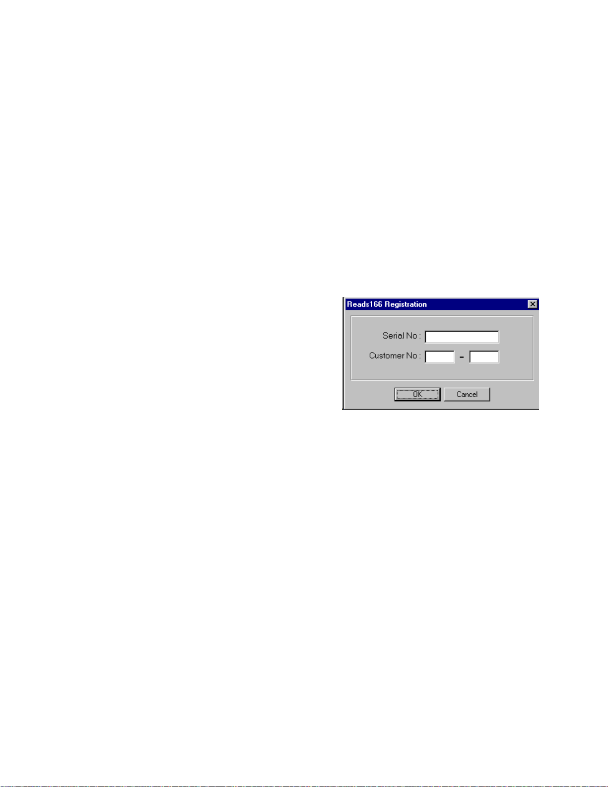
3.3.1 Demo Version
When you run the READS166 software a pop-up registration box will open asking for your serial
and customer numbers. If you are using the demo
version of the software you may press CANCEL
and the box will disappear and the About Box will
appear. Press the OK button in the About Box and
the software will run in the Demo mode. The demo
mode limits the size of the files you can compile to
about 8K.
3.3.2 Full Version
If you’ve purchased the READS166 software a
registration sheet with the serial number and customer number will be included with the
READS166 User’s Guide. When you run the READS software insert these numbers in the correct
boxes, press OK and then press OK in the About Box. Your software is registered and ready to
use.
3.4 Configuring READS166 and Initiating Host-to-Board Communicati ons
1. Press the Projects | Options | Project Properties | HW Configuration to select the
board you are using from the list. Or using the Tools | Hardware Configuration menu
command, choose the name of the board you are using from the board list which appears.
- -4
Page 11

2. Open the TTY window using the Tools | TTY menu command. Select the communication
port parameters using the Tools | TTY | TTY Options menu command. You will need to
select the COM port you are using, and the baud rate.
3.5 Bootstrapping
In the default configuration, all monitor programs are downloaded to the boards after the boards
are bootstrapped. That is, there is no ROM on the board that is executed upon reset.
Bootstrapping loads a small monitor, called MinMon, which in turn loads a larger monitor
- -5
Page 12

RMON16x. Once the monitor program is loaded, the monitor commands are available to the
user.
1. Press the reset button on the board.
2. From the menu in the TTY window select TTY | Bootstrap and Download Monitor. The
board will now bootstrap and download the monitor program.
You may observe the bootstrap progress in the status line of the TTY window. When
bootstrapping is completed, the READS166 monitor prompt appears in the TTY window.
3.6 Verifying that the Monitor is Loaded
Make sure the TTY window is active, clicking the mouse inside the TTY window to activate it if
necessary. Then type the letter ‘H’ (case insensitive) to verify that the monitor program is
responding. The ‘H’ command displays the available single-letter commands the monitor will
recognize.
The READS monitors use single-letter commands to execute basic functions. Port configurations
and data, as well as memory inspection and modifications may be accomplished by the monitor.
Most of the single-letter commands are followed by 4 hexadecimal digit addresses or 2
hexadecimal digit data bytes. The following is a list of the commands.
R E A D S C O M M A N D S
C nn Read port nn Configuration (DPnn)
C nn=mmmm Set port nn Configurat ion (DPnn=mmmm)
D Download HEX file
G XXXX Go, execute code at XXXX
H Help, display this list
M XXXX Memory, contents of XXXX
M XXXX=nn Memory, change contents of XXXX to nn
M XXXX-YYYY=nn Memory, change block XXXX-YYYY to nn
P nn Read Port nn (Pnn)
P nn=mmmm Write to Port nn (Pnn=mmmm)
W XXXX Word memory, contents of XXXX
W XXXX=mmmm Word memory, change contents of XXXX to mmmm
W XXXX-YYYY=mmmm Word memory, change block XXXX-YYYY to mmmm
- -6
Page 13

3.7 Troubleshooting
All the boards are functionally tested before shipment. If the system does not bootstrap as
expected, review the hardware, software, and PC setup.
3.7.1 Hardware Set-up
1. Make sure that that you have the power connected correctly.
2. Verify that the power-on LED is lit.
3. Review the jumper settings.
4. Check the modem cable connections to the board and to the host PC.
5. Run the READS software and try to bootstrap and download the monitor again.
If the board still won’t operate correctly, check the software setup.
3.7.2 Software Set-up
1. Select the TTY menu TTY Option.
2. Verify that the COM port correctly matches that of the host PC.
3. Select the Baud rate to be 19.2K
4. Select a large TTY Timeout parameter, one of at least 2 seconds.
5. Note the hardware configuration given in the drop list “HW Configuration.”
6. From the Reads166 main window, select the menu option Hardware Configuration located
under the Tools menu.
7. Find the record corresponding to the hardware configuration selected in the TTY Options.
8. The Name, Processor, Board, and Description fields are for information purposes only. If the
fields are not as listed above, you may search for a record which matches the desired fields.
Once located, go to the TTY Options dialog and select the correct hardware configuration.
Alternatively, you may create a new hardware configuration record or modify an existing one
from the Hardware Configurations dialog.
If the board still won't operate correctly, check the PC setup.
3.7.3 PC set-up
1. Go to the Windows Control Panel usually located under the Settings menu (Start, Settings,
Control Panel).
2. Click on the Ports icon. (If one does not exist, you may need to install some Windows
components again.)
3. Select the port you are using. If the port number does not appear in the list add the port by
clicking on the “Add” button. You need to restart Windows for the new port selection to take
effect.
4. Click on the “Settings” button.
5. Select 57600 Baud, 8 data bits, no parity and 1 stop bit. Set “Flow Control” to none.
6. Click on the “Advanced” button. Select the port you are using.
7. Specify the “Base I/O Port Address” and the “Interrupt Request Line (IRQ)” fields to be
“default.”
8. You should try both enabling and disabling FIFO.
If these steps do not remedy the problem, please contact Rigel Corporation at (352) 3734629 or http://www.rigelcorp.com.
- -7
Page 14

4 OPERATING NOTES
The RMB-167 needs two connections: to a 5 volt well regulated power supply and to the serial
port of a host via a modem cable.
4.1 Power
Power is brought to the RMB-167 board by a two-position screw-type terminal block. A well
regulated 5 volt DC source is required. The (+) and (-) terminals are marked on the board. Note
that a diode is placed across the input in reverse. Thus if the power is applied to the RMB-167
board in reverse polarity, the diode will short the power supply attempting to prevent damage to
the board. Populated with 64K of CMOS RAM, the RMB-167 draws less than 175 mA.
4.2 Serial port 0
Serial port 0 is accessed through the RS-232 level converter U11. The microcontroller supports
the transmit and receive signals. A minimal serial port may be constructed with just 3 lines:
transmit, receive, and ground, disregarding all hardware handshake signals. Port P1 (HOST) of
the RMB-167 is a DB-9 female connector used to connect the board to an IBM compatible PC. A
straight-through modem cable may be used. That is a cable connecting pin 2 of the RMB-167 to
pin 2 of the host, and similarly pin 3 to pin 3, and pin 5 to pin 5. This cable and a DB9-DB25
adapter is supplied when the board is purchased directly from Rigel Corporation. JP11 is a 3-pin
header, which carries the same signals as P1. It is convenient if the board is to be used as an
embedded controller. JP11 is also denoted by S0, and its 3 lines by G (Ground), T (Transmit),
and R (Receive) on the RMB-167 silk-screen.
4.3 Serial Port 1
Serial port 1 is used as a synchronous serial channel by the SAB-C167. It has 3 TTL-level
signals, MRST (Master Receive Slave Transmit). MTRS (Master Transmit Slave Receive), and
SCLK (Serial Clock). Header JP12 carries these three signals as well as provides VCC and GND
for reference. Header JP12 is also denoted by SSC (Serial Synchronous Channel) on the silkscreen. The individual pins of the header are denoted by VCC, R, T, C, and GND, which
correspond to VCC, MRST, MTSR, SCLK, and GND, respectively.
4.4 Jumper Selection
Two jumpers are needed to use the RMB-167 in the default 64K/256K RAM and no EPROM
mode. These should be placed at the Options jumper JP3 corresponding to P0.4 and P0.6. The
jumper at P0.4 invokes the bootstrap mode upon a reset. P0.6 selects the bus configuration.
4.5 LEDs
The RMB-167 has three LEDs. The red LED, when lit, shows power is connected to the board.
The yellow LED is an auxiliary LED, whose state is determined by the GAL equations. For
example the user may program the yellow LED to indicate the presence of a program in EPROM.
The default PAL equations set the yellow LED to be the complement of the green LED.
The green LED indicator marked RO (Reset Out) is connected to a GAL device. The LED is
turned on after system initialization is completed. More specifically, the LED is turned on when
the RSTIN# is high and RSTOUT# makes a 0-to-1 transition, which normally follows an EINIT
instruction.
The LED RO will be off and remain off until the bootstrap loader successfully completes loading
the bootstrap file into RAM.
- -8
Page 15

5 MEMORY OPTIONS
The RMB-167 memory decoding is accomplished by two 16V8-type GAL devices, U1 and U2.
Both devices are collectively responsible of selecting the options of determining the memory map.
An output of U1, AUX0 is an input to U2. Similarly, AUX1 connects the two devices. The signal
on AUX1 may flow in either direction, giving a wide range of possible ways to divide the
functionality between the two devices. A slide switch is also provided to allow switching between
alternate memory maps. The GAL inputs include RSTIN# and RSTOUT#, so that a memory map
swap upon completion of the reset process is possible, as explained in the Siemens Application
Notes. The RMB-167 decodes the address lines A13 to A17. Thus the memory map may be
constructed in blocks of 16K. For example, EPROM may occupy only the lower 16K of memory,
whereas RAM occupy the remaining addresses. The GAL equations for the default configuration
are given in Section 5.1.
5.1 RAM Memory Options
Either 32K 62C256-type or 128K 681000-type static RAM chips may be used. Two chips are
needed, one for EVEN and the other for ODD addresses.
5.2 EPROM Memory Options
The RMB-167 has sockets to accommodate two 27C256-type 32K EPROMS. Two chips are
needed, one for EVEN and the other for ODD addresses. The EPROMS may be configured to
occupy low memory, high memory, or start at low memory and then relocate to high memory upon
initialization by appropriate jumper selections.
The SAB C167 may be programmed to insert wait cycles during external memory access.
However, in order to run the SAB C167 at its full potential of 40MHz, the RAMs should be rated at
70 nano seconds or faster, and the EPROMs should be rated at 85 nano seconds or faster.
5.3 Alternate Memory Map with EPROM in Low Memory
The default RMB-167 memory map uses only the RAM chips. That is the range 0 to FFFFh is
decoded as RAM. The addresses are decoded by a GAL device. Alternate memory maps are
possible by changing the GAL programs. Moreover, several jumper inputs allow switching
between memory maps by changing jumper configurations. One possible implementation is given
below. Other memory maps are possible with different GAL equations.
The jumpers marked CFG0 and CFG1 are used to switch between the memory maps as shown
below. In words, CFG0 determines the memory type for the lower 32K of memory, and CFG1, the
higher. Inserting a jumper selects EPROM. The GAL equations to achieve the alternate memory
maps are given in Section 5.2.
- -9
Page 16

Address Range
Jumpers
inserted
none RAM RAM
CFG0 EPROM RAM
CFG1 RAM EPROM
CFG0 and
CFG1
The EPROM at low memory may contain start-up code which is executed upon reset. In this case
the jumper at P0.4 must be removed so that the microcontroller does not enter the bootstrap
loader mode. The microcontroller simply starts executing from address 0.
With the jumpers CFG0 or CFG1 (or both) installed, the RMB-167 may still be bootstrapped.
Again, the jumper P0.4 must be installed. This forces the SAB-C167 to enter the bootstrap mode
upon reset. The bootstrap sequence terminates with a software reset instruction which starts
executing the program starting at address 0. With CFG0 installed, this is the beginning of
EPROM. That is, upon bootstrap, the code in EPROM is executed. While possible, first
bootstrapping and then executing the code in EPROM is somewhat superfluous since any
initialization code of the bootstrap loader may be placed in EPROM.
0-7FFFh 8000h-FFFFh
EPROM EPROM
5.4 Moving RMON167 to EPROM
As an example of placing a valid program in EPROM, consider modifying the monitor program
RMON167 as given below. It is assumed that the lower 32K of memory is EPROM, and the
higher 32K is RAM. The origin of the program is changed to 1000h. Note that the monitor needs
buffers to store the commands and the parameters. These buffers are defined to occupy the
beginning of RAM at 8000h. Also, the greeting message is changed to indicate that it is the
EPROM version of the monitor.
Only the beginning few instructions and the greeting message are changed. Namely,
1. The buffers are moved to 8000h and 8020h, respectively,
2. Jump statements are placed at RESET and NMI vectors,
3. The origin of the monitor program is moved to 1000h
4. The initialization to CPS is now accomplished by an inter-segment jump to 1010h,
5. And finally, the greeting message is changed.
Also note that the address of register SYSCON is different in the SAB80C166 and SAB C167
microcontrollers. The monitor program must be assembled by specifying the C167 register
definitions. The program listing follows.
CODE0 section code AT 0000h
; r15 is used for flags:
; bit 0 - error
; 1 - dash
; 2 - equal
; 3 ;--------------------------------------------------; --- monitor system variables ---
- -10
Page 17

; --- !!! ASSUMES 8000h-FFFFh is RAM !!! --; org 08000h
cmdbuf equ 08000h
pbuffr equ 08020h
;---------------------------------------------------
org 0 ; RESET vector
RSTISR proc near
jmp cc_UC, mon ; branch to monitor
RSTISR endp near
org 00008h ; NMI vector
NMISR proc near
jmp cc_UC, mon ; branch to monitor
NMISR endp near
; -------------------------------------------------org 01000h
; -------------------------------------------------; --- monitor program ---
MON proc near
mov SYSCON, #0F800h ; #1111 1000
; 0000 0000 b
nop
mov SYSCON, #0F800h ; #1111 1000
; 0000 0000 b
nop
; --- initialize CPS -------------------------------
;0xFA 0x00 0x10 0x80 ; jmps far 1000h ;
(jump to next1) ; far intersegment jump to update CPS
;next1:
dw 000FAh
dw 01010h
next1:
; --- initialize DPPx ----------------------------- mov DPP0, #0
.
.
( no changes to the code here )
.
.
; --------------------------------------------------;--- message
strings --; -------------------------------------------------EVEN
msggreet:
db 0ah, 0dh, ’SAB-C167 MONITOR IN EPROM > ’, 0
.
.
.
( no changes to the code here )
As mentioned, the address of register SYSCON is different (89h) in the C167. The instruction
setting the SYSCON register is a move instruction. In machine code, the instruction takes four
bytes: E6h, 89h, 00h, F8h, which may be hand-coded as,
- -11
Page 18

; mov SYSCON, #0F800h
; SYSCON is 89h on the 167
dw 089E6h
dw 0F800h
nop
; mov SYSCON, #0F800h
; SYSCON is 89h on the 167
dw 089E6h
dw 0F800h
- -12
Page 19

6 GAL EQUATIONS
Two PALCE16V8 are used. The first (U1) is responsible for the reset logic and auxiliary options,
and the second (U2), for the memory decode logic. Refer to the circuit diagrams for more
information.
6.1 Default GAL Equations
6.1.1 U1 Equations
;U1 Bootstrap Loader Logic
;----------------- PIN Declarations --------------; --- inputs --PIN 1 A18 COMBINATORIAL ;
PIN 2 A19 COMBINATORIAL ;
PIN 3 A20 COMBINATORIAL ;
PIN 4 A21 COMBINATORIAL ;
PIN 5 A22 COMBINATORIAL ;
PIN 6 A23 COMBINATORIAL ;
PIN 7 RSTIN_ COMBINATORIAL ;
PIN 8 RSTOUT_ COMBINATORIAL ;
PIN 9 CFG0 COMBINATORIAL ;
PIN 11 CFG1 COMBINATORIAL ;
; --- outputs --PIN 12 HISEG COMBINATORIAL ;
PIN 13 RSTCYC COMBINATORIAL ;
PIN 14 RSTCYC_ COMBINATORIAL ;
PIN 15 AUX0 COMBINATORIAL ;
PIN 16 AUX1 COMBINATORIAL ;
PIN 17 DUMMY COMBINATORIAL ;
PIN 18 LEDRST_ COMBINATORIAL ;
PIN 19 LEDAUX_ COMBINATORIAL ;
;----------------- Boolean Equation Segment -----EQUATIONS
RSTCYC = /( RSTIN_ * RSTCYC_ )
RSTCYC_ = /( /RSTOUT_ * RSTCYC )
HISEG = A18 * A19 * A20 * A21 * A22 * A23
AUX0 = 1
AUX1 = 1
DUMMY = 1
LEDRST_ = RSTCYC
LEDAUX_ = RSTCYC_
- -13
Page 20

6.1.2 U2 Equations
; U2 Memory Decode Logic
;----------------- PIN Declarations --------------; --- inputs --PIN 1 A0 COMBINATORIAL ;
PIN 2 A14 COMBINATORIAL ;
PIN 3 A15 COMBINATORIAL ;
PIN 4 A16 COMBINATORIAL ;
PIN 5 A17 COMBINATORIAL ;
PIN 6 BHE_ COMBINATORIAL ;
PIN 7 MON COMBINATORIAL ;
PIN 8 HISEG COMBINATORIAL ;
PIN 9 RESET COMBINATORIAL ;
PIN 11 AUX0 COMBINATORIAL ;
PIN 19 AUX1 COMBINATORIAL ;
; --- outputs --PIN 12 RAMSELL_ COMBINATORIAL ;
PIN 13 RAMSELH_ COMBINATORIAL ;
PIN 14 ROMSEL_ COMBINATORIAL ;
PIN 15 MA14 COMBINATORIAL ;
PIN 16 MA15 COMBINATORIAL ;
PIN 17 MA16 COMBINATORIAL ;
PIN 18 MA17 COMBINATORIAL ;
;----------------- Boolean Equation Segment ------
EQUATIONS
RAMSELL_ = A0
RAMSELH_ = BHE_
ROMSEL_ = 1
MA14 = A14
MA15 = A15
MA16 = 0
MA17 = 0
6.2 Alternate GAL Equations
6.2.1 U1 Equations For EPROM In Low Memory
;PALASM Design Description
; EPROM/RAM selected by CFG0 and CFG1
;
;
; jumper at low 32K high 32K
; ----------- ------- -------; NONE RAM RAM
; CFG0 EPROM RAM
; CFG1 RAM EPROM
;CFG0 and CFG1 EPROM EPROM
; --- Declaration Segment ---------------------------TITLE RMB-167 Memory Decode Logic -- RAM/EPROM
PATTERN
REVISION
AUTHOR
- -14
Page 21

COMPANY Rigel Corporation
DATE 07/20/94
CHIP _r167u1 PALCE16V8
; --- PIN Declarations --------------------------------; --- inputs --PIN 1 A18 COMBINATORIAL
PIN 2 A19 COMBINATORIAL
PIN 3 A20 COMBINATORIAL
PIN 4 A21 COMBINATORIAL
PIN 5 A22 COMBINATORIAL
PIN 6 A23 COMBINATORIAL
PIN 7 RSTIN_ COMBINATORIAL
PIN 8 RSTOUT_ COMBINATORIAL
PIN 9 CFG0 COMBINATORIAL
PIN 11 CFG1 COMBINATORIAL
; --- outputs --PIN 12 HISEG COMBINATORIAL
PIN 13 RSTCYC COMBINATORIAL
PIN 14 RSTCYC_ COMBINATORIAL
PIN 15 AUX0 COMBINATORIAL
PIN 16 AUX1 COMBINATORIAL
PIN 17 DUMMY COMBINATORIAL
PIN 18 LEDRST_ COMBINATORIAL
PIN 19 LEDAUX_ COMBINATORIAL
; --- Boolean Equation Segment -----------------------
-EQUATIONS
RSTCYC = /( RSTIN_ * RSTCYC_ )
RSTCYC_ = /( /RSTOUT_ * RSTCYC )
HISEG = A18 * A19 * A20 * A21 * A22 * A23
AUX0 = CFG0
AUX1 = CFG1
DUMMY = 1
LEDRST_ = RSTCYC
LEDAUX_ = RSTCYC_
;-----------------------------------------------------
6.2.2 U2 Equations For EPROM In Low Memory
;PALASM Design Description
; CFG0 and CFG1 select RAM and EPROM
;
; jumper at low 32K high 32K
; ----------- ------- -------; NONE RAM RAM
; CFG0 EPROM RAM
; CFG1 RAM EPROM
;CFG0 and CFG1 EPROM EPROM
; --- Declaration Segment ----------------------------
-TITLE RMB-167 Memory Decode Logic
PATTERN
REVISION
AUTHOR
COMPANY Rigel Corporation
DATE 09/14/94
CHIP _r167u2 PALCE16V8
- -15
Page 22

; --- PIN Declarations --------------------------------; --- inputs --PIN 1 A0 COMBINATORIAL
PIN 2 A14 COMBINATORIAL
PIN 3 A15 COMBINATORIAL
PIN 4 A16 COMBINATORIAL
PIN 5 A17 COMBINATORIAL
PIN 6 BHE_ COMBINATORIAL
PIN 7 MON COMBINATORIAL
PIN 8 HISEG COMBINATORIAL
PIN 9 RESET COMBINATORIAL
PIN 11 AUX0 COMBINATORIAL
PIN 19 AUX1 COMBINATORIAL
; --- outputs --PIN 12 RAMSELL_ COMBINATORIAL
PIN 13 RAMSELH_ COMBINATORIAL
PIN 14 ROMSEL_ COMBINATORIAL
PIN 15 MA14 COMBINATORIAL
PIN 16 MA15 COMBINATORIAL
PIN 17 MA16 COMBINATORIAL
PIN 18 MA17 COMBINATORIAL
; --- Boolean Equation Segment ----------------------EQUATIONS
RAMSELL_ = A0 + (A15+/AUX0) * (/A15+/AUX1)
RAMSELH_ = BHE_ + (A15+/AUX0) * (/A15+/AUX1)
ROMSEL_ = (A15+AUX0) * (/A15+AUX1)
MA14 = A14
MA15 = A15
MA16 = A16
MA17 = A17
; ----------------------------------------------------
- -16
Page 23

7 HEADERS AND JUMPERS
7.1 System and I / O Headers
The RMB-167 board has three headers, two of which are compatible with those of the RMB-166.
The two RMB-166 headers, the input output port header JP2 and the system header JP1, are
similar to the headers JP6 and JP7 of the RMB-167. In addition, the RMB-167 has JP8, the Extra
Input/Output header XIO. Ports 2, 3, and 5 are available on JP7. JP6 contains the address, data
and control busses. JP8 contains the additional ports and signals of the SAB-C167
microcontroller. Individual signals of these jumpers are listed below. The tables reflect the
physical orientation of the headers and the enumeration of their individual posts. Pin 1 is
identified as the post with the square pad on the circuit board.
JP6 - System Header
Signal Pins Signal
RMB-
166
(JP1)
Ground 1 2 VCC (+5V)
Ground 3 4 VCC (+5V)
RSTIN# 41 42 WR# WR# /
RSTOUT# 43 44 BHE#
A22 not
A21 not
RMB-
167
(JP6)
D0 5 6 A0
D1 7 8 A1
D2 9 10 A2
D3 11 12 A3
D4 13 14 A4
D5 15 16 A5
D6 17 18 A6
D7 19 20 A7
D8 21 22 A8
D9 23 24 A9
D10 25 26 A10
D11 27 28 A11
D12 29 30 A12
D13 31 32 A13
D14 33 34 A14
D15 35 36 A15
RD# 37 38 A16
ALE 39 40 A17
NMI# 45 46 not
47 48 not
used
49 50 not
used
RMB-
166
(JP1)
used
used
used
RMB-
167
(JP6)
WRL#
A18
A19
A20
- -17
Page 24

Note that pins 46-50 on the RMB-167 are not connected to any signal.
JP7 - Input/Output Header
Signal Pins Signal
RMB-
166
(JP2)
Ground 1 2 VCC (+5V)
Ground 3 4 VCC (+5V)
VAGND 15 16 S1I not
VAREF 17 18 S1O not
RMB-
167
(JP7)
P5.0 5 6 P5.1
P5.2 7 8 P5.3
P5.4 9 10 P5.5
P5.6 11 12 P5.7
P5.8 13 14 P5.9
P2.0 19 20 P3.0
P2.1 21 22 P3.1
P2.2 23 24 P3.2
P2.3 25 26 P3.3
P2.4 27 28 P3.4
P2.5 29 30 P3.5
P2.6 31 32 P3.6
P2.7 33 34 P3.7
P2.8 35 36 P3.8
P2.9 37 38 P3.9
P2.10 39 40 P3.10
P2.11 41 42 P3.11
P2.12 43 44 P3.12
P2.13 45 46 P3.13
P2.14 47 48 P3.14 not
P2.15 49 50 P3.15
RMB-
166
(JP2)
RMB-
(JP7)
used
used
used
167
- -18
Page 25

JP8 - Extra Input/Output Header of the RMB-167
Signal Pins Signal
RMB-167 RMB-167
Ground 1 2 VCC (+5V)
Ground 3 4 VCC (+5V)
P6.0 5 6 P6.1
P6.2 7 8 P6.3
P6.4 9 10 P6.5
P6.6 11 12 P6.7
A23 13 14 READY#
VAGND 15 16 not used
VAREF 17 18 not used
P5.0 19 20 P7.0
P5.1 21 22 P7.1
P5.2 23 24 P7.2
P5.3 25 26 P7.3
P5.4 27 28 P7.4
P5.5 29 30 P7.5
P5.6 31 32 P7.6
P5.7 33 34 P7.7
P5.8 35 36 P8.0
P5.9 37 38 P8.1
P5.10 39 40 P8.2
P5.11 41 42 P8.3
P5.12 43 44 P8.4
P5.13 45 46 P8.5
P5.14 47 48 P8.6
P5.15 49 50 P8.7
Note that Port 5 pins P5.0 to P5.9 are available on the Input/Output Header JP7 as well as on the
Extra Input/Output Header JP8. Pins 16 and 18 on the header JP8 are not connected to any
signal.
- -19
Page 26

7.2 Analog-to-Digital Converter Reference Jumpers
The analog-to-digital converter requires a ground and reference voltage. These reference
voltages may be provided either from JP2 lines marked VG (ground reference voltage) and VR
(reference voltage), or connected to the +5 volt TTL supply. Jumpers JP4 and JP5 select the
source of reference voltages. The center posts of JP4 and JP5 are connected to the SAB-C167
VAREF and VAGND inputs. Post 1 of JP4, marked VCC is connected to the +5 volt supply.
Thus, connecting this post with the center post selects VAREF to be the same as the +5 volt
supply. In the alternate position, VAREF is to be supplied from JP7 from the terminal marked VR.
Similarly, the post marked GND of JP5 is connected to the ground of the supply. Connecting the
center post of JP5 with the post marked GND selects VAGND to be the same as the ground of
the supply voltage. In the alternate position, the ground reference is to be supplied from the JP7
terminal marked VG.
- -20
Page 27

8 BOOTSTRAPPING
The RMB-167 bootstrapping is triggered by grounding P0L.4 at reset. A 16 pin header is used to
ground the bits of P0L via a resistor array with a nominal value in the range of 22K to 33K.
Note that the GAL which controls the bootstrap load operation is also responsible for turning on
the LED. In its default implementation, the LED is lit once the RSTOUT# signal is activated. For
specific applications, the user may alter the operation of the bootstrap logic by changing the GAL
equations.
Once the bootstrap loader is invoked the serial port S0 is used to communicate with the C167.
The host must first send a 0 byte with 8 data bits, 1 stop bit and no parity bits. The C167
responds with the byte A5h . Then the host expects 32 bytes of code to be downloaded to
internal RAM starting at address 0FA40h and run.
Since 32 bytes is not enough to initialize and configure the C167 and then download a user
program, a secondary loop is used. This loop is a short piece of code that is placed starting at
address 0FA60h, so that when the 32 bytes of primary code are executed, the program continues
with the secondary loop. The approach is described in more detail below.
The 32 bytes downloaded are, in hexadecimal,
E6 F0 60 FA
9A B7 FE 70
A4 00 B2 FE
7E B7
B4 00 B0 FE
86 F0 BB FC
3D F6
CC 00
CC 00
CC 00
CC 00
which correspond to the following short code.
; origin is 0FA40h
mov R0, #0fa60h
W0:
jnb S0RIR, W0
movb [R0], S0RBUF
bclr S0RIR
movb S0TBUF, [R0]
cmpi1 R0, #0fcbb ; read 604 bytes
jmpr cc_NE, W0
nop
nop
nop
nop
- -21
Page 28

Note that the NOP (no operation) operations are required to fill the 32 bytes, since the bootstrap
loader remains active until all 32 bytes are received. When the bootstrap loader receives its last
byte and places it in address 0FA5Fh, it makes a jump to 0FA40h and starts executing the code.
This is the short loop given above. Note that at this time the internal RAM starting from 0FA60h
does not contain any relevant code.
The short loop takes advantage of the serial port S0 which is already initialized. It waits for a user
specified number of bytes, 604 bytes in this case, and places these bytes consecutively starting
from internal RAM location 0FA60h. When the loop is done (all 604 bytes received) the program
continues by executing the NOP operations, and then executing code from 0FA60h on. Thus the
604 bytes loaded by the secondary loop are also interpreted as code.
The user may alter the number of bytes to be loaded by changing the 21st and 22nd bytes (BB
and FC) which give the address (the low byte, followed by the high byte) of the last byte to be
read by the loop. Note that there is a practical limit to the number of bytes that can be
downloaded by this loop: the PEC source and destination pointers as well as the SFRs which
occupy addresses FDE0h and above must not be overwritten by data bytes.
Due to the powerful instruction set of the C167, a lot of functionality can be implemented within
604 bytes of code. The 604 bytes contained in the file BTL67.DAT downloads a minimal monitor
program. This program contains an initialization routine, subroutines to send and receive
characters through the serial port, a subroutine to download code in the Intel Hex format, and a
subroutine to jump to any location within the 64K segment. The latter two are invoked by singleletter commands.
The 604 byte-code may be broken down into four sections.
1. Initialization code to be executed after the 32-byte bootstrap
2. Code to be written starting at address 0 to be executed after the software reset.
3. The minimal monitor to be placed starting at address 8000h
4. The software reset (SRST) instruction to leave the bootstrap mode.
Sections 1 and 4 are somewhat different than sections 2 and 3. The bytes downloaded in
sections 1 and 4 are actual instructions which are executed after the 32-byte bootstrap load is
completed. Sections 2 and 3 are instructions to poke bytes into memory. More specifically, in
section 2, bytes are written to memory locations starting from address 0. In section 3, from
address 8000h. The bytes placed into memory locations starting from address 0 is executed after
the software reset instruction. This is an initialization program which, upon completion, branches
to address 8000h to execute the minimal monitor program.
For example, the initialization code starting at address 0 begins with the two instructions
DISWDT
EINIT
whose machine instructions are (A5 5A A5 A5) and (B5 4A B5 B5),
- -22
Page 29

respectively. The code within the 604-byte download block pokes these bytes starting from
address 0. That is, these instructions are placed into memory, one word at a time, as data. The
following instructions are used.
mov R1, #0A55Ah ; begin: DISWDT
mov 0, R1
mov R1, #0A5A5h
mov 2, R1
mov R1, #0B54Ah ; EINIT
mov 4, R1
mov R1, #0B5B5h
mov 6, R1
This pattern is used throughout sections 2 and 3. First the word is written to register R1. Then
the register is copied to memory. The file BTL67.DAT contains the bytes downloaded to the
RMB-167 board during bootstrapping. The file BTL.SRC contains the source code.
The initialization routines configure the SYSCON register. The internal ROM is disabled and the
external bus is activated. Next the CSP and DPP registers are initialized. These steps need to
be completed before the EINIT instruction. Note that if the watchdog timer is to be disabled; this
too must be done before the EINIT instruction.
- -23
Page 30

9 THE MINIMAL MONITOR
The minimal monitor is placed by the bootstrap loader starting at address 8000h. The monitor
responds to two single-letter commands ’D’ and ’G’. The ’D’ command places the monitor in a
download mode. Code in the Intel Hex format is expected. Code may be downloaded anywhere
in the first 64L segment. The ’G’ (Go) command expects 4 hexadecimal characters. These 4
characters specify an address within the first 64K segment. A jump is performed to this address.
If a user program is downloaded (using the ’D’ command), say at address 0C000h, then the
GC000 command branches to the user program. In many cases, the user program is the
application program or a monitor program, such as RMON167, and hence, the minimal monitor is
no longer required. If, however, the user program wishes to return to the minimal monitor, it
should branch to address 8000h. Note that the minimal monitor initializes the stack, so either a
call or a jump to address 8000h would work.
The minimal monitor is a loop that executes the following flowchart:
- -24
Page 31

9.1 MON167 Monitor
The monitor program RMON167 allows inspecting and modifying the first 64K segment of RMB167 memory, configuring the ports, inputting and outputting from the general purpose ports,
downloading code in the Intel Hex format, and branching to user code. RMON167 features are
invoked by single-letter commands. RMON167 assumes a 20MHz (40 MHz) system crystal.
Serial port 0 is initialized to run at 9600 Baud with 8 bits of data, 1 stop bit and no parity bits.
RMON167 is intended to be downloaded after bootstrapping the RMB-167 board. RMON167 is
placed starting at address 0C000h. The first 256 bytes are reserved for monitor variables. The
entry point to RMON167 is at address C100h. To set up RMON167, initialize READS166 and the
RMB-167 board and invoke the Bootstrap command as explained in the previous section. From
the TTY menu, select Download to download RMON167.HEX. Branch to and execute
RMON167 using the Run command under the TTY menu. Specify address C100 since the entry
point to RMON167 is at 0C000h. Note that RMON167 places a jump to C100 at the nonmaskable
interrupt vector. Thus, RMON167 may subsequently be invoked by pressing the NMI pushbutton
on the RMB167-CRI. RMON167 initializes the stack and resets the interrupts. Thus, even after
the NMI button is pressed, RMON167 clears the NMI interrupt by executing a dummy ’return from
interrupt’ instruction.
Alternatively, RMON167 may be placed in EPROM and invoked upon reset. The source code for
RMON167 is given on the distribution disk. RMON167 is not optimized for speed or size, but
rather for clarity and pedagogical value. The legal users are encouraged to modify RMON167
and use portions of it in applications programs.
The single-letter commands of RMON167 are explained below.
D Download HEX file
The D command places RMON167 in a download mode. The monitor expects to receive code in
the Intel Hex format through serial port 0. The download mode is terminated when the last line of
Intel Hex code is received (when the byte count is 0).
C Port Configuration
The C command is used to configure the ports, i.e., the port direction registers DPnn. Cn displays
the current setting of DPn. Cn=mmmm writes the word mmmm to register DPn.
GGo
The user code at address xxxx is branched to by the Gxxxx command. Note that the user
program may return to RMON167 by a branching instruction to address 0C000h. RMON167
initializes the stack, thus, either a jump or a call instruction may be used to return to RMON167.
HHelp
The H command displays a summary of available monitor commands.
MMemory
The first 64K segment of the RMB167-CRI memory may be inspected or modified by the M
command. The M command is also useful to poke short programs into memory.
M XXXX displays the current contents of memory address XXXX.
M XXXX=nn inserts the byte nn into memory address XXXX. When this command is used,
RMON167 displays the current contents as well as the new contents. The address XXXX is
incremented and the current contents of (XXXX+1) are displayed. Consecutive bytes may be
written starting at XXXX. The process is terminated if a carriage return or an illegal hexadecimal
digit is keyed in.
M XXXX-YYYY displays the block of memory between addresses XXXX and YYYY.
M XXXX-YYYY=nn fills the memory block XXXX to YYYY with byte nn.
- -25
Page 32

P Port Data
The P command is used to read from or write to the ports. Pn displays the current value of port n.
If port n is an input port, then the value read is the current voltage levels applied to the ports. If
port n is an output port, Pn retu rns the current output value to port n. Pn=mmmm sets the current
value of output port n to mm.
Note that individual bits of the ports may be programmed as input or output. Thus, the word
returned by Pn gives the external voltage levels applied to the input bits and the current values of
the output bits.
W Word Memory
This command is identical to the M command, except that the memory contents are displayed and
modified as words (2 bytes). Words start at even address.
- -26
Page 33

10 READS166 VERSION 3.0
READS166, version 3.00, is Rigel Corporation’s Integrated Development Environment for the
SGS Thomson 16-bit processors. READS166 includes an editor, a host-to-board
communications system, an assembler, and a C compiler. READS166 is completely rewritten in
native 32-bit code to run on Windows95 and WindowsNT. READS166 includes a sophisticated
project management system to simplify code reusability and version control. The C compiler is
rewritten to support a full debugger. The debugger allows you to step through your code with
breakpoints and variable watches as the compiled code runs on the target board, similar to the
operation of an in-circuit emulator.
RMON166 - The READS166 monitor program
RMON 166 is downloaded after bootstrapping (or it may be placed into ROM) and supports basic
memory and port functions. RMON166 allows downloading and running applications programs.
The complete source code for user modifications or upgrades is included on disk.
Ra66 - The READS166 Assembler
Ra66 is a cross assembler for the C166 family of microcontrollers. It is intended to be used by
the hardware and software products available from Rigel Corporation. Ra66 is a two-pass
assembler. Forward references are resolved during the second pass. The second pass is used
only when necessary. If no forward references are used, Ra66 completes assembly in a single
pass.
Rc66 - The READS166 C Compiler
Rc66 is a C Compiler for the C166 family of processors. It compiles code for the tiny memory
model which fully resides in the first segment of memory. Rc66 is a designed as a low-cost C
compiler which provides a quick development cycle for simpler applications which do not need
more than 64K of code, or the use of standard C libraries. Rc66 implements a subset of ANSI C.
Rc66 works in conjunction with Ra66: first an assembly language program is generated from the
C source then a HEX file is created.
The READS166 software has the following distinctive features:
• Project management for organized software development
• Archive storage for source code modules
• Multiple project management with drag and drop module transfers
• Enhanced graphical user interface for easy monitoring
• Stand alone compiler and editor applications connected to READS166 in a client/server
fashion
• Drag and drop code development
• Mixed mode projects (C and assembler)
• Wizard code generator
10.1 READS166 V3.00 CONCEPTS
READS166 introduces a project-oriented code development and management system. The new
concepts are defined below.
10.1.1 Project
A project is collection of files managed together. Each file in a project corresponds to a code
module. All projects are kept in their individual subdirectories. You may copy or save projects as
a single entity. When saved under a different name, a new subdirectory is created and all
components of the project are duplicated in the new subdirectory.
- -27
Page 34

By using the long names provided by the 32-bit Windows operating systems, you may use this
feature to keep different versions of your software in a controlled manner. For example, the
project “Motor Control 07-20-1997” may be saved under the name “Motor Control 07-25-1997” as
new features are added. This way, if needed, you may revert to an older version.
A project may either be an “executable project” or an “archive project.”
10.1.1.1 Executable Projects
Executable projects are meant to be compiled into code which is eventually run on the target
system. Components of an executable project are the code modules containing subroutines or
functions which make up the entire program.
10.1.1.2 Archive Projects
Archive projects are never compiled. They are intended to facilitate code reusability by organizing
and keeping code modules together. An archive project acts as a repository which you may add
modules to, or copy modules from. Executable projects can be quickly constructed using already
written and debugged modules from an archive project.
10.1.2 Module
A module is a single file which belongs to a project. Typically modules are either assembly
language subroutines or C language functions. You may copy modules from one project to
another, or share modules in different projects. For example, you may copy a previously
developed module from an archive project to an executable project by simply dragging its icon
from one project window to the other. By using existing or previously developed and debugged
modules, you may significantly improve code reusability, much in the same manner as libraries.
Reusing modules differs from using library functions of existing routines in that modules are kept
in source form rather than object form.
For more information on the READS166 software please refer to the READS166
Version 3.0 Users Manual. The manual is also available in PDF format from our
Web site www.rigelcorp.com.
- -28
Page 35

11 CIRCUIT DIAGRAMS
- -29
 Loading...