

Page 1

TCL
SERVICE MANUAL
EU MT/ SERIALS
1. Caution…………………………………………………………………………2
2. Specification …………………………………………………………………6
3. Block Diagram..................................................................................................7
4 . Alignment Procedure…………………………………………………………8
5. Scheme Diagram…………………………………………………………… 18
This manual is the la test a t the time of p rinting, an d does not
include the modification which may be made after the printing, by
the constant improvement of product
Page 2

RISK OF
ELECTRIC
SHOCK DO
NOT
OPEN.
SCHNEIDER ELECTRONICS GMBH-GERMANY
1. CAUTION
CAUTION:
Use of controls, adjustments or procedures other than those specified herein may result in
hazardous radiation exposure.
CA UTION: TO RE DU CE TH E RIS K OF
CA U T ION
RISK
SHOCK
The lighting flash with arrowhead symbol, with an equilateral triangle is intended to
alert the user to the presence of uninsulated voltage within the products
enclosure that may be of sufficient magnitude to constitute a risk of electric shock to
the person.
The exclamation point within an equilateral triangle is intended to alert the user to the
presence of important operating and maintenance (servicing) instructions in the
literature accompanying the appliance.
ELECTRI
NOT
OPEN.
ELECTR ICAL SHOCK, DO NOT RE MOVE
COVER (OR BACK). NO USER SERVICEABLE
PAR TS INS IDE . RE FE R SER VIC ING TO
QUALIFIE D SERVIC E PERSONNEL.
dangerous
WARNING: TO REDUCE RISK OF FIRE OR ELECTRIC SHOCK, DO NOT
EXPOSE THIS APPLIANCE TO RAIN OR MOISTURE.
2
2
Page 3

SCHNEIDER ELECTRONICS GMBH-GERMANY
IMPORTANT SAFETY INSTRUCTIONS
CAUTION:
Read all of these instructions. Sa ve these instructions for later use . Follo w all Warnings and
Instructions marked on the audio equipment.
1. Read Instructions-All the safety and operatinginstructionsshouldbe read before the productis operated.
2. Retain Instructions- The safety and operating instructions should be retained for future reference.
3. Heed Warnings- All warnings on the product and in the operating instructions should be adhered to.
4. Follow Instructions- All operating and use instructions should be followed.
FOR YOUR PERSONAL SAFETY
1. When the power cord or plug is damaged or frayed, unplug this television set from the wall outlet and refer servicing to
qualified service personnel.
2. Do not overload wall outlets and extension cords as this can result in fire or electric shock.
3. Do not allow anything to rest on or roll over the power cord, and do not place the TV where power cord is subject to
traffic or abuse. This may result in a shock or fire hazard.
4. Do not attempt to service this television set yourself as opening or removing covers may expose you to dangerous
voltage or other hazards. Refer all servicing to qualified service personnel.
5. Never push objects of any kind into this television set through cabinet slots as they may touch dangerous voltage
points or short out parts that could result in a fire or electric shock. Never spill liquid of any kind on the television set.
6. If the television set has been dropped or the cabinet has been damaged, unplug this television set from the wall outlet
and refer servicing to qualified service personnel.
7. If liquid has been spilled into the television set, unplug this television set from the wall outlet and refer servicing to
qualified service personnel.
8. Do not subject your television set to impact of any kind. Be particularly careful not to damage the picture tube surface.
9. Unplug this television set from the wall outlet before cleaning. Do not use liquid cleaners or aerosol cleaners. Use a
damp cloth for cleaning.
10.1. Do not place this television set on an unstable cart, stand, or table. The television set may fall, causing serious injury
to a child or an adult, and serious damage to the appliance . Use only with a cart or stand recommended by the
manufacturer, or sold with the television set. Wall or shelf mounting should follow the manufacturer s instructions, and
should use a mounting kit approved by the manufacturer.
10.2. An appliance and cart combination should be moved with care. Quick stops, excessive force, and uneven surfaces
may cause the appliance and car t combination to overturn.
3
3
Page 4

SCHNEIDER ELECTRONICS GMBH-GERMANY
PROTECTION AND LOCATION OF YOUR SET
11. Do not use this television set near water ... for example, near a bathtub, washbowl, kitchen sink, or laundry tub, in a
wet basement, or near a swimming pool, etc.
Never expose the set to rain or water. If the set has been exposed to rain or water, unplug the set from the wall
outlet and refer servicing to qualified service personnel.
12. Choose a place where light (artificial or sunlight) does not shine directly on the screen.
13. Avoid dusty places, since piling up of dust inside TV chassis may cause failure of the set when high humidity persists.
14. The set has slots, or openings in the cabinet for ventilation purposes, to provide reliable operation of the receiver, to
protect it from overheating. These openings must not be blocked or covered.
Never cover the slots or openings with cloth or other material.
Never block the bottom ventilation slots of the set by placing it on a bed, sofa, rug, etc.
Never place the set near or over a radiator or heat register.
Never place the set in enclosure, unless proper ventilation is provided.
a built-in
PROTECTION AND LOCATION OF YOUR SET
15.1. If an outside antenna is connected to the television set, be sure the antenna system is grounded so as to provide some
protection against voltage surges and built up static charges, Section 810 of the National Electrical Code, NFPA No.
70-1975, provides information with respect to proper grounding of the mast and supportingstructure, grounding of the
lead-in wire to an antenna discharge unit, size of grounding conductors, location of antenna discharge unit, connection
to grounding electrode, and requirements for the grounding electrode.
EXAMPLE OF ANTENNA GROUNDING AS PER NATIONAL ELECTRICAL CODE INSTRUCTIONS
EXAMPLE OF ANTENNA GROUNDING AS PER
NATIONAL ELECTRICALCODE
ANTENNA
LEAD- IN WIRE
GROUND CLAMP
ELECTRIC SERVICE
EQUIPMENT
NEC-NATIONAL ELECTRICALCODE
ANTENNA DISCHARGE
UNIT (NEC SECTION
810-20)
GROUNDING
CONDUCTORS
(NECSECTION 810-21)
GROUND CLAMPS
POWER SER VICE GROUNDING
ELECTRODE SYSTEM
(NEC ART 250. PART H)
15.2. Note to CATV system installer : (Only for the television set with CATV reception)
This reminder is provided to call the CATV system attention to Article 820-40 of the NEC that provides
installer s
guidelines for proper grounding and, in particular, specifies that the cable ground shall be connected to the grounding
system of the building, as close to the point of cable entry as practical.
16. An outside antenna system should not be located in the vicinity of overhead power lines or other electric lights or power
circuits, or where it can fall into such power lines or circuits. When installing an outside antenna system, extreme care
should be taken to keep from touching such power lines or circuits as contact with them might be fatal.
17. For added protection for this television set during a lightning storm, or when it is left unattended and unused for long
periods of time, unplug it from the wall outlet and disconnect the antenna. This will prevent damage due to lightning
and power-line surges.
4
4
Page 5

SCHNEIDER ELECTRONICS GMBH-GERMANY
OPERATION OF YOUR SET
18.
This television set should be operated only from the type of power source indicated on the marking label.If you are not
sure of the type of power supply at your home, consult your television dealer or local power company. For television
sets designed to operate from battery power, refer to the operating instructions.
19. If the television set does not operate normally by following the operating instructions, unplug this television set from the
wall outlet and refer servicing to qualifiedservice personnel. Adjust only those controls that are covered in the operating
instructions as improper adjustment of other controls may result in damage and will often require extensive work by a
qualified technician to restore the television set to normal operation.
20. When going on a holiday : If your television set is to remain unused for a period of time, for instance, when you go on
a holiday, turn the television set and unplug the television set from the wall outlet.
off
IF THE SET DOES NOT OPERATE PROPERLY
21. If you are unable to restore normaloperationby followingthedetailedprocedurein your operating instructions,
do not attempt any further adjustment. Unplug the set and call your dealer or service technician.
22. Whenever the television set is damaged or fails, or a distinct change in performance indicates a need for
service, unplug the set and have it checked by a professional service technician.
23. It is normal for some TV sets to make occasional snapping or popping sounds, particularly when being
turned on or off. If the snapping or popping is continuous or frequent, unplug the set and consult your
dealer or service technician.
FOR SERVICE AND MODIFICATION
24. Do not use attachments not recommendedby the television set manufacturer as they may cause hazards.
25. When replacementparts are required, be sure the service technician has used replacement parts specified
by the manufacturer that have the same characteristics as the original part. Unauthorized substitutions
may result in fire, electric shock, or other hazards.
26. Upon completion of any service or repairs to the television set, ask the ser vice technician to perform
routine safety checks to determine that the television is in safe operating condition.
5
5
Page 6

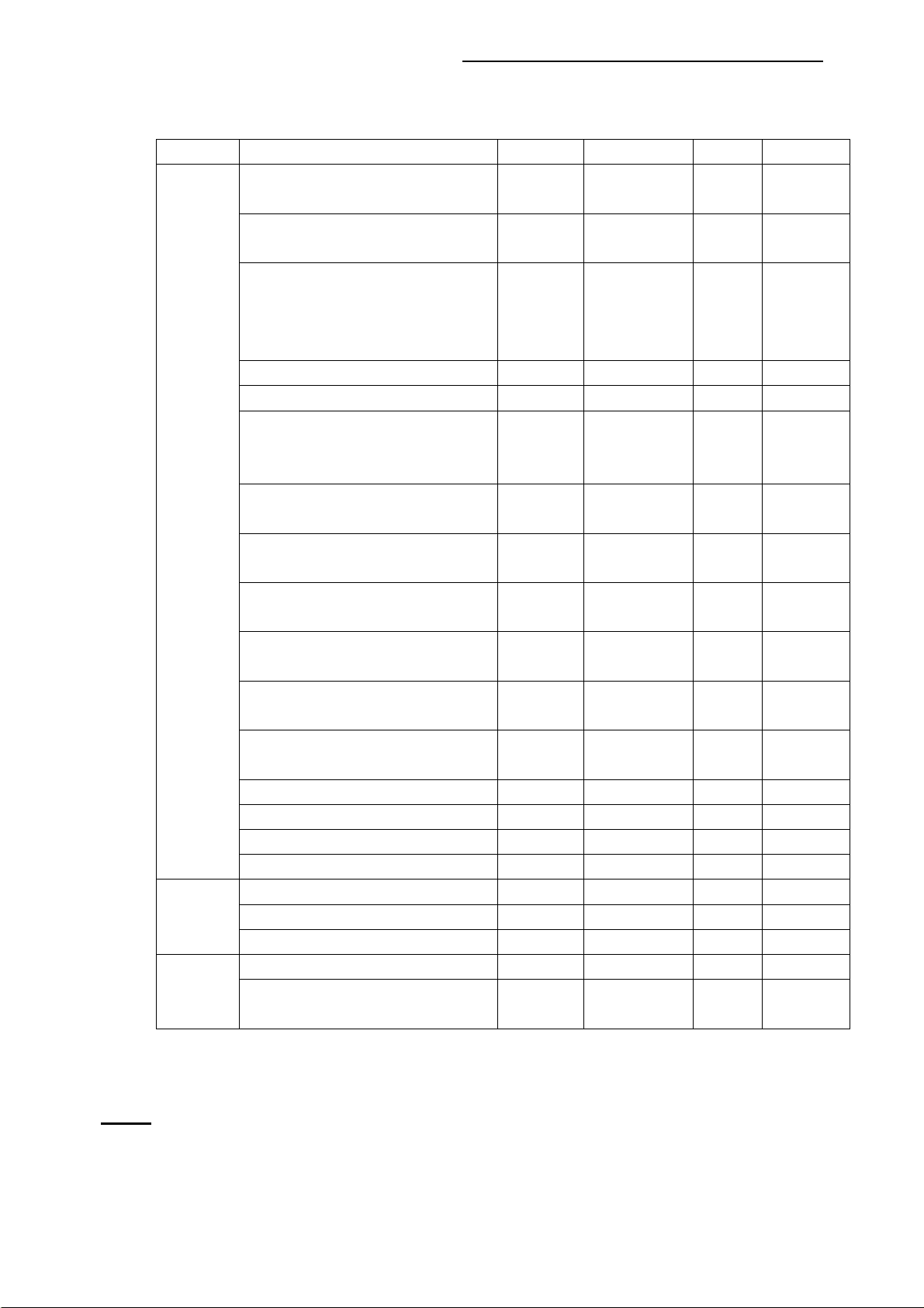
Key Features
Update:2010/04/7 V:1.1
机芯号 Model #
使用范围: TCL/中国大陆
★低成本模拟电视
★USB多媒体(图片、音乐)
★HDMI1.3接口*2
主要功能特点
★睡眠定时 1.切台或换信源黑屏.
主要芯片 Main IC
处理芯片
型号 Module
MT8223H
功能定义:
图像
动态背光
动态对比度
色温调整 Adjustable Color Temperature
比例模式 Format Control
背光调节 Backlight Adjust
梳状滤波Comb Filter
降噪Noise Reduction
声音SOUND
声音功率Audio Power (Watts) Front Speakers
音效 新闻、电影、音乐、标准、自设定共五种
平衡
均衡 高低音
智能音量 Yes
音响单独听
信号格式SIGNAL FORMAT CAPABILITY
射频格式 RF Tuning Capability
AV制式 AV Formats (PAL/NTSC/SECAM)
YPbPr最高格式
HMDI最高格式
VGA支持分辩率:
点对点显示(VGA、YPbPr、HDMI)
电视功能
频道数 channel quantity 99
频道跳跃
智能搜台
频道互换
其它 同公司标准
多媒体/娱乐 Yes
音乐播放 Yes MP3
图片播放(数码相册)
音画播放
系统功能
睡眠定时
OSD语言 中文简体/英语 EM语言根据需求另定
OSD时间调节 固定
开机LOGO 标准 标准LOGO
能效及认证
待机功耗 --
能效等级 --
节能认证
环保证认
4:3、全屏(16:9)、宽屏、16:9字幕 自适应 共
MT23H
Yes
Yes
Yes
五种
Yes
3D
3D
8W/CH x 2
Yes
Yes
PAL(I/D/K/B/G)
PAL/NTSC/SCAM
1080P
1080P
1920*1080
Yes
Yes
Yes
Yes
Yes
Yes
Yes
Yes
No 符合中国ROHS要求
备注
JEPG
摇控器REMOTE CONTROL
摇控器型号 Remote Model Number
码值格式 RCA 38K
键数
Yes
RC300
37
后端子 CONNECTIONS — REAR
HDMI
Dsub15 VGA
VGA音频 Audio input for Dsub 15 VGA Φ3.5*1
分量输入 Composite Video input(HDTV)
分量音频 Component Aideo Input (YCrCb/YPrPb) (synchroscan)
AV input
RF Input (PAL)
AV输出 AV Output
1
1
1
1R+1L
1 AV (AV1)
1
1 AV
侧置端子 FAV
AV input
HDMI
USB
1(AV2)
1
1
第1页共1页
Page 7

Page 8

Factory Alignment Specification of normal SIACP
TCL WW R&D
FPD CENTER
Factory Alignment Specification of normal SIACP
For MT8223 serial
For the following Chassis:
MT8223L:
MT8223H:
Version:V0.1
PREPARED BY : LiuShuBiao DATE : 2010-05-13
APPROVED BY : DATE :
Page 1 of 10
Page 9

Factory Alignment Specification of normal SIACP
Disclosure
The information contained in this document is proprietary to TCL SZ FPD lab and shall not be
disclosed by the recipient to third persons without the written permission of the team leader or
GM of R&D.
Revision History
Status, Ver Date, Drafter Description of changes
V0.10 2010-02-07 This is the first version of normal SIACP
·HDMI as the main absolute input
·The password of factory menu is 9735
Page 2 of 10
Page 10
Factory Alignment Specification of normal SIACP
These chassises are designed for ALL GLOBE LCD TV. The main chip is from Mediatec
(MT8223 series) and supports below inputs and outputs:
class item MT8223L MT8223H
ATV
( PAL B/G D/K I)
DTV
(DVB-T,DVB-C,DVB-S)
HDMI
(480i/p, 576i/p, 720p up to
1080i/p, compliant v1.3. with
HDCP)
VGA
VGA/DVI audio
CMP
(YPrPb can support from 480i up
to 1080p,au
input
&
output
function
Others
Serial connector of MT8223 definition:
Pin1:VCC Pin2:RXD Pin3:TXD Pin4:GND
SCART1
(CVBS & RGB,audio)
SCART2
(CVBS & YC,audio)
Side AV or back AV
(CVBS,audio)
USB player
(picture,video,audio)
SCART1 output
(CVBS,audio)
SCART2 output
(CVBS,audio)
Headphone output
SPDIF output
AV out 1 1
MEMC
CI+
Serial connector
I2C connector of MEMC
module
dio)
√ √
1 2
1 1
1 1
1 1
1/1 1/1
Picture
audio
Coaxial Optical
P001 P001
Picture,
audio
INFO:
ª All tests and measurements mentioned hereafter have to be
(220 ~ 240 VAC)TBD
ª All voltages have to be measured with respect to
carried out at a normal mains voltage
ground, unless otherwise stated
Page 3 of 10
Page 11

Factory Alignment Specification of normal SIACP
ª All final tests have to be done on a complete set including LCD panel in a room with temperature of
25+/-7°C
ª The White Balance (color temperature) has to be performed i
least 1 hour of warm-up/burn-in. This is applicable for both Alignment and Picture Performance
evaluation at OQA in order to be set free of any temperature drift ( colorimetry vs time)
nto subdued lighted room after at
1. Electrical Assembly Alignment
1.1. Preconditions – DC/DC Check
Before power on, please check the board according to the relevant block diagram and circuit
diagram, and make sure
that no serious error should destroy the board. For example,the output
of DC/DC and LDO should not shorted to ground.
Supply a suited voltage and power on , then check the voltage according to the relevant block
diagram , circuit diagram and volt
voltage for main chip(AVDD3V3, DVDD3V3,
age spec . the error should less than 5% .For example, the
VCCK,etc.), the voltage for DDR (DDRV) , the
voltage for amplifier(AUDIO_PWR),etc. Only the standby voltage is necessary if there is no
software in the flash .
1.2. SW download
Download the latest release MT8223_SW into the flash using MTK SW tool. See Appendixo
“How to download FLASH SW”. Or upgrade the SW from USB port See Appendixp” Ho
w to
upgrade FLASH SW from USB”.
1.3. Panel ID check and modify
There is different ID stored in the NVM depended on different Panels. Modify it with Hyper
terminal if the initial ID or a wrong ID make the set can not display clearly. See Appendixr
. It can
be checked and modified in Factory menu->Feature->Panel ID if the set can display clearly .
The set should be restart if the panel ID is changed .
1.4. Functional Test
Once the boards (chassis, KB, IR, PSU…) and the panel are well interconnected, connect all
external generator devices to relevant input
patterns format and check picture content and sound quality accordingly
Source Test signal
Analog Tuner RF cable Full Band (VHF/UHF) + CATV
Composite(CVBS) Chroma/Fluke PAL Half Color & Gray bars
VGA Chroma/QuantumData 1024x768@60Hz
CMP (YPrPb) Chroma/QuantumData 1080i@60Hz
HDMI DVD with HDMI compliancy Movie 720p@60Hz
Headphone RF cable First channel
Loud Speakers RF cable First channel
(generator) Test pattern (format/image)
s/outputs below according to their respective test
:
Half Color & Gray bars
Half Color & Gray bars
Audio tones can be defined by the factory (ie: 1KHz & 3KHz, sweep, …).
Picture video formats can be changed by the factory according to their own st
andard.
1.5. ADC Calibration
To ensure the ADC performance, the error of “generator+cable” must be less than 2%. The
Page 4 of 10
Page 12

Factory Alignment Specification of normal SIACP
following inputs require an ADC calibration for the time being.
VGA(skip this step if no VGA input on the chassis)
Provide a test signal 1024×768@60Hz with WhiteBlack squares.
Select the corresponding Factor
yMenu->
ADC -> Auto ADC , then press ”OK” key on
RemoteControl to start. Value of status will change to “OK” if succeed.
CMP
Provide a test signal 720p@60Hz with 100% 8 steps ColorBar.
Select the corresponding Factor
RemoteControl to start. Value of status will change to “OK” if succeed.
Scart RGB(skip this step if no SCART input on the chassis)
Provide a test signal PAL 576i with 100 % 8 steps ColorBar.
Select the corresponding Factor
RemoteControl to start. Value of status will change to “OK” if succeed.
The mean of status value:
“NONE”= n
“OK”= curr
“NOK
“ALL”= all input
o input is successful in ADC calibration.
ent input is successful in ADC calibration.
”= current input is fail in ADC calibration.
s required are successful in ADC calibration.
R Gain, G Gain, B Gain, R Offset, G Offset, B Offset in FactoryMenu-> ADC page can be
fine-tuned if necessary but not required.
yMenu->
yMenu->
ADC -> Auto ADC , then press ”OK” key on
ADC -> Auto ADC , then press ”OK” key on
1.6. DDC & EDID Test
The E-EDID data structure are according to VESA
HDMI).
Both VGA and HDMI have their own separate bin files:
For EDID check, it’s needed to check whether the correct EDID is down
corresponding EDID NVM Checksum or read them out to check bit by bit if it is in line with the
released EDID bin file.
Enhanced EDID 1.3 (and EIA/CEA-861B for
loaded by checking
1.7. HDCP Test
For HDCP compliancy, it’s needed to check whether the HDCP key has been well set.
1.8. CI+ Key activation and test(This step is only for the models with CI+ function )
(FOR EU MODEL)
Select factory menu-> Up
RemoteControl to active the CI+ KEY. The Valid(CI+ state) state turn to “Yes” and Cus
on
Code(Custom Code), Serial Num display if succeed. Download the CI+ Key and try to active it
again if fail.
date CI+ Credential-> Update CI+ Credential , then press ”OK” key
2. Final Assembly Alignment
2.1. FactoryMenu
Follow the below steps to pop-up the Factory Menu in case of “Factory
press RemoteControl key “MENU” to display main menu
-
Key” is disable
:
Page 5 of 10
Page 13

Factory Alignment Specification of normal SIACP
- Select “Picture” and press “OK” key to enter the picture submenu
- Select “Contrast” item
press the subsequence RemoteControl keys “9”, “7”, “3” and “5”
-
Press RemoteControl key “Retu
enable.(TBD)
rn” To pop-up the Factory Menu in case of “HotKey” is
The status of “HotKey” can be changed in FactoryMenu-> HotKey
Press
RemoteControl “OK” key or “RIGHT” key to enter the submenu.
Press RemoteControl “Menu
Press RemoteControl “RIGHT”or “
Press RemoteControl “OK” key run the function.
Press RemoteControl “Exit” key exit the factorymenu.
” key to go back to the root menu.
LEFT” key to change the values.
2.2. Entering to “P” Mode
Turned on the factory key to enter into “P” mode.The TV will display “P” in bottom left corner
P” mode.
in “
2.3. White Balance Alignment
Make sure that the picture mode is “vivid”, enter to “P”
switch off “Pic. Enhance” in Factory Menu-> WD Alignment before white balance alignment .
VGA,CMP,SCART RGB,CVBS_P
CVBS_SECAM and CVBS_NTSC C
Warm and Cool Color Co
Only HDMI(
YUV 720p@60Hz) input requires color temperature adjustment.
ordinates are relatives to Normal mode.
AL Color Coordinates are relative to HDMI.
olor Coordinates are relative to CVBS_PAL.
mode(
turned on the factory key) and
All the Relative
Matrix Offsets should be set while doing alignment.
Expected Targets and Tolerances
The measured parameters should be “x, y” coordinates.
The White Balance alignment should be perfo
CA-210). The analyzer may not touch the screen surface, and measurement must be performed in a
dark environment keeping the probe(s) at 90+/-2° from the panel.
The result should measure up the releva
The alignment have to fulfill the requirement
nt spec.
rmed using a contact less analyzer (ei: Minolta
s in Application Form.
Alignment FlowChart
Provide a test signal on the input and align the WB as described inside attached document
ensuring first that the BackLight value is matching below table:
2.4. High Pot. and Insulating Resistance Tests
At the end of the process, a High Pot. and an
Insulating Resistance tests are required for
Page 6 of 10
Page 14

Factory Alignment Specification of normal SIACP
matching Safety Electrical requirements (ei: xxxx)
High Voltage Withstanding requirements
- “Voltage” Ö 3500 VAC
- “Max Leakage Current” Ö
- “Test Time” Ö
10 mA
5 sec
Insulating Resistance requirements
- “Voltage” Ö DC500V
- “Threshold Max” Ö
- “Threshold Min” Ö 4MΩ
- “Test Time” Ö
3 sec
3. Factory default settings
Do the “Shop init” before packing.The detail of reset shop follow OOB setting.
“Factory Menu” Definition
1). HotKey
Item Sub-item
OFF:Factory Key is invalidation
ON :Factory Key is a
key.
OFF:
ON :
vailability, and “RETURN” key is the shortcut
2). W
ADC
3).
4).WB
Hotkey
arm up
Item Sub-item
Warm up
Item Sub-item
ADC
ADC Source YPbPr1 / VGA
Auto ADC DO / WAIT / OK
R GAIN
G GAIN
B GAIN
R OFFSET
G OFFSET
B OFFSET
Item Sub-item
WB
BalanceSource AV1\ VGA\ HDMI1
Color Temp Cool \ Normal\ Warm
R GAIN
G GAIN
Page 7 of 10
Page 15

5).Shop In
it
Item Sub-item
Shop Init DO / WAIT / OK
6).NVM Reset
Item Sub-item
NVM
Reset
7).Pre Channel
Item Sub-item
Pre
Channel
8).Po
werMode
Item Sub-item
Power
Mode
9).Design
Menu1
Item Sub-item
DesignM
enu1
Factory Alignment Specification of normal SIACP
B GAIN
R OFFSET
G OFFSET
B OFFSET
WB Init DO / WAIT / OK
Auto ADC DO / WAIT / OK
Pattern Off / On
PATTERN LUMA 0-255
DO / WAIT / OK
VOL_0 HuiZhou\ TTET \WUXI
ON\ last \Standby
InitVol 0--100
PicPreset User\ Standard\ Soft\ Vivid
BacklightPreset 0--100
TunerAGC (default value is0)
Project ID
Pattern
See appendix○
Pattern1\Pattern2\Pattern3\Pattern4\
4
Pattern4\ PatternCose
PrintMessage
Sound Count
DBC
DB_CP
Off/On
0—255
Page 8 of 10
Page 16

10).DesignMenu2
Item Sub-item
DesignM
enu2
11).Sound Curve
Item Sub-item
Sound
Curve
Factory Alignment Specification of normal SIACP
DBC_BP
Panel Control On/Off
Panel Freq 0-255
Panel Percent
0-255
BlueMute On/Off
OtherCTI On/Off
FleshTone
LumaControl
Hotel Menu
USB UPG
BackIT
Vol_1
Vol_10
Vol_20
Vol_40
Vol_50
Vol_70
Vol 100
TV Pre
AV Pre
I2S
On/Off
On/Off
On/Off
USB download software
On/Off
12).Version
Item Sub-item
Version Prj. Project ID
Ver. SW Vx.x
Panel Mode
PSU
SIACP_VER
Date Month Date Year
Appendix o “How to download FLASH SW”
Prepare MTK SW tool for update.
1. Connect the PC to the serial connector on board using a
COMx).
Page 9 of 10
special serial device (USB or
Page 17

2. Provide the a correct voltage to the board
3. Start “MTKT
picture(notice:select MT8223 chassiss):
OOL.exe” application under MTKxx folder, and set the parameters as below
Factory Alignment Specification of normal SIACP
4. Press “Browse” button to select the co
5. Press “Upgrade” button to start downloading the SW and wait the gauge displayed “100%”
that means the SW has been successfully dow
In the meanwhile, all operations such erasing fla
window script.
6. Once the SW is downloaded, switch-off/on the chassis board and w
eeprom update.
rresponding SW bin file to upload
nloaded.
sh and so… are parsed into the debug
ait few seconds for
See Appendixp” How to upgrade FLASH SW from USB”
Upgrade with loader:
1. Save the new software file(*.bin) in the root directory of USB, and modify it’s name as
upgrade.bin. (The file name must be one of the” TCLCNH、TCLCNL、TCLAPH、TCLAPL、
TCLLAH、TCLLAL” and should be same as the file name on the model)
2. Select
Upgrade without loader(The TV set should be able to display normally):
1. Save the new software file(*.bin) in the root directory of USB, and modify it’s name as
2. Plug in the USB.
3. Press the “Program +” for a long time.
Factory Menu—>DesignMenu2—>USB UPG,Then press “OK” key on the remote.
upgrade.pkg.
Page 10 of 10
Page 18

8 7 6 5
4 3 2 1
F
E
D
HDMI CEC
HDMI SCL
PWR5V-IN
HDMI HPD
JTRST#
JTDO
JTCK
VGA-SDA/JTMS
VGA-SCL/JTDI
OPWRSB
ADIN0
ADIN3
RF-AGCO
BOOST PWM
U1TX AU-SWA
BL-Dimming
BL ON/OFF
LVDS PWR CTRL
LVDS CTRL0
RXD1 PIN41:GPIOL[0]
HDMI-PC0 PIN241:GPIOE[0]
HDMI_SW2/SCL
HDMI_SW1/SDA
function defineGPIO
HDMI CEC
HDMI SCL
HDMI SDLHDMI SDL
HDMI power detect
HPD to source device(fall edge)
JTAG/A ALL mute(power on/off mute)
JTAG/SYS-EDID-WP(L WP)
JTAG/AU-AMP-MUTE(H AMP Mute)
JTAG/VGA-SDA
JTAG/VGA-SDA
POWER Module on(L)/off(H) Control
SCT1-FS
KEY pad
RF AGCO
Boost PWM for tuner 30v
AU-SWBU1RX
Backlight Dimming
BL ON/OFF
LVDS PWR CTRL(H POWER Enable)
LVDS CTRL0
PIN240:GPIOE[1]
PIN239:GPIOE[2]
key
LED & IR Socket
HDMI P202
EEPROM U003
8223L
AV2 P305
SCART & AV OUT P303&P302
YPBPR L/R P301
LVDS Socket
spi flash u001
XTAL
VGA P201
POWER
TUNER
TU1 TU2 U503
Main power P101
AMP TPA3113D2
U601
AUDIO OUT P601
USB P203
P304
AV1
F
E
D
sheet1
sheet2
POWER TREE BLOCK
sheet3
sheet4
sheet5
sheet6
sheet7
C
3.3V/5VSTB
LDO #1
RT9116
3.3VSTB
32.59mA
document
power supply
8223L,Flash/XTAL/JTAG/UART,Backlight
HDMI,USB,VGA
AV/YPbPr/Audio MUX
Speaker/Line out/Mute
LVDS/ Tuner
C
Main power supply
SDR_V=2.5v
423mA
ON/OFF
From MT8223L
AS1117
LDO #4
DVDD3V3 /3.03mA
B
LDO #5
VCCK=1.1V
367mA
RT9042
B
DC/DC
12V/24
MP1482
LDO #6
AS1117
A
THIS DRAWING CANNOT BE COMMUNICATED TO UNAUTHORIZED PERSONS COPIED UNLES S PERMITTED IN WRITING
5V-TUNER
80mA
+5V
760mA
LDO #2
AS1117
AVDD3V3
332mA
LDO #3
AS1117
Index-Lab
5
AVDD1V25
125.74mA
DATE
Last saved :
SBU :
TCLNO:
DESCRIPTION Last modifNAME
3-25-2010_21:26
4678
MT22/21/20 MAIN SCHEMATIC
.............
TCL Thomson Electronics Singapore Pte. Ltd.
8 Jurong Hall Road #28-01/06
The JTC Summit SINGAPORE 609434
DESIGNATION
DRAWN
DESIGNATION
3 2 1
TCL MULTIMEDIA TECHNOLOGY HOLDINGS LTD
ON:
BY:
04-13-2009
......
Tel (65) 63092900 Fax (65) 63092999
CHECKED
ON:
BY:
PAGE:
OF :
A
4
7
FORMAT DIN A2
Page 19

8 7 6 5
4 3 2 1
L103
0R
+12V_IN
10U
C114
GND
D103
LL4148
NC
C115
1U
R120
4K7
Q104
BT3904
+5V
R116
1K
GND
F
GND
R117
10K
NC
R119
100R
NC
C
E
R121
10K
B
GND
R122
100R
C117
33P
BL_DIMMING
E
+5VSB
C111
T
PB-ADJ
0.1U
+24/12V
GND
T
GND
BL-ADJUST
L102
0R
Z6
T
+24/12V
GND
PB-ON/OFF
PW-ON
C108
1000P
T
3.3/5VSB
T
GND
+12V_IN
GND
PW-ON
GND
2
10
C109
1000P
P101
+12V_IN+12V_IN
1
34
56
78
9
1112
GND
GND
GND
3.3/5VSB
F
STANDBY POWER for 19&22
R101
0R
NC
+5VSB
C101
4U7
NC
GND
C102
0.1U
U101
RT9166-33
3
IN OUT
GND
GND
1
2
C103
4U7
GND
Z3V3
C104
0.1U
STBV3V3
T
SW
Q102
BT3904
+5VSB
C
E
GND
R104
2K7
B
0.1U
C105
GND
1K
R105
OPWRSB
R106
10K
BL_ON/OFF
R107
1K
R108
22K
C106
1000P
DVDD3V3DVDD3V3
GND
+5V+5V
C110
GND
1000P
SW
C107
0.1U
R109
1K
PB-ON/OFF
L101
C
B
Q103
BT3904
E
GND
GND
R110
4K7
T
0
NC
+24/12V
+5VSB
GND
+5VSB
Z2
C113
0.1U
Z3
GND
GND
GND
T
R112
0R
0.1U
T
PB-ADJ
R111
0R
C112
E
ANALOG POWER AVDD3V3
4
4
+5V
C118
100U
GND
C119
0.1U
16V
U103
AS1117-3.3
VIN
GND/ADJ
OUT
1
2
3
GND
C120
100U
GND
16V
3V3
AVDD3V3 DVDD3V3
T
0R
C121
0.1U
R126
D
VCCK POWER
47U
GND
U104
AS1117AD
10V
C135
0.1U
DRAM POWER
+5V
C134
C
VIN
4
4
GND/ADJ
OUT
2
3
R152
330R
GND
R151
330R
1
C136
100U
GND
SDR2V5
C137
0.1U
16V
SDR_V
T
10U
C148
SDR_V
+5V
For 26&32 Model
R146100K
C168
0.1U
8
SS
7
EN
B
5
FB
0.1U
C165
3300P
C166
C167
0.1U
R145
2K2
U108
BS
SWCOMP
GND
MP1482
C172
1
2
IN
36
4
0.1U
SR34
D102
NC
L114
15UH
GND
ANALOG POWER AVDD1V25
U105
AS1117AD
C139
C138
0.1U
100U
16V
U106
1
PGOOD
2
EN
3 6
VIN VOUT
4
VDD
RT9042
+5V
L112
0
0
L113
C171
0.1U
R1532R7
R1492R7
1V0SB
C169
470U
16V
R147
51K
R148
11K
AVDD3V3
16V
100U
GND
+12V
C143
C142
0.1U
GND
5V_OUTSIDE
C170
470U
16V
GND
R135100K
GND
GND
ADJ
NC
VIN
5V
T
4
4
GND/ADJ
OUT
2
3
8
7
5
R131
0R
GND
GND
R130
120R
1
16V
C141
0.1U
C140
100U
GNDGND
R133
22K
R134
10K
R132
0R
VCCK1V1
C144
0.1U
47U
GND
1V25
C145
10V
AVDD1V25
T
T
0R
VCCK
R150
C122
220U
+24/12V
C123
35V
1U
GND
C124
0.1U
C125
1U
GND
C126
0.1U
D105
LL4148
RT8110B
BOOTFBUGATE
5
VIN
7
8
GNDPHASE
LGATE
VCC
U102
4
36
2
1
C127
2U2
GND
4
S2
3
G1
S1
G2
2
1
Q101
D13N03LT
D2B
D2A
D1B
D1A
5
6
7
8
R123
C128
0.033U
For >=32 Model
L104
10UH
2R2
GND
R124
5K1
R125
360R
GND
C129
0.015U
C130
470U
+12V_IN
16V
C131
10U
GND
16V
12V
T
C132
0.1U
0R
0R
+12V
R113
R114
D
C
SW
10K
R139
NC
0.1U
C039
GND
+5VSB
+24/12V
R138
22K
NC
R137
10K
NC
B
NC
GND
C146
NC
1U
C
Q106
BT3904/NC
E
For 19&22 Model
NC
LL4148
G
G
R136
820K
NC
D106
S
D
5V_OUTSIDE
Q107
PMV65XP/NC
S
PMV65XP/NC
Q108
D
NC
C147
0.22U
C156
0.1U
NC
+12V
+12V
B
GND
GNDGND
GND
GND
A
THIS DRAWING CANNOT BE COMMUNICATED TO UNAUTHORIZED PERSONS COPIED UNLES S PERMITTED IN WRITING
SBU :
TCLNO:
MT23H MAIN SCHEMATIC
.............
TCL Thomson Electronics Singapore Pte. Ltd.
8 Jurong Hall Road #28-01/06
A
The JTC Summit SINGAPORE 609434
DESIGNATION
ON:
BY:
DRAWN
04-13-2009
......
Index-Lab
DATE
DESCRIPTION Last modifNAME
DESIGNATION
Last saved :
5
4-1-2010_20:32
4678
3 2 1
TCL MULTIMEDIA TECHNOLOGY HOLDINGS LTD
Tel (65) 63092900 Fax (65) 63092999
CHECKED
PAGE:
ON:
BY:
OF :
1
9
FORMAT DIN A2
Page 20

8 7 6 5
4 3 2 1
STBV3V3
R018
4K7
F002
F001
AVDD1V25
0R
0.1U
C013
GND
AVDD3V3_CVBS
0.1U
GND
120R
C023
0.1U
L003
120R
R049 0R
1
2
3
4
GND
P001
AVDD3V3
R052
1R
AVDD3V3
R054 0R
C017
10U
C018
AVDD3V3_XTAL_STB
GND
AVDD3V3_VGA_STB
C026
0.1U
GND
AVDD1V25_HDMI
0.1U
C033
GND
F
E
D
C
B
R017
21
R020
V270RA
C038
10U
Z1
T
4K7
T
Z002
R051
AVDD3V3_LVDS
X27
10U
GND
NC
27M
Near IC
C020
27P
R00410K
OXTALO
+5V
NC
C004
GND
R003
22K
0.047U
RF_AGC
R002 100K
NC
+5VSB
R060
1K
S_CE
DVDD3V3_SPI
Flash
+12V
R062
5K6
GND
OXTALI
C019
27P
0.1U
C002
GND
C003
U001
O0N
VCCK
AVDD1V25
O0P
O1N
O2N
O1P
OCKP
OCKN
O3N
O3P
E0N
E0P
E1N
E1P
E2N
AVDD3V3_LVDS
F
SDR_V
SDR_V
VCCK
SDR_V
VCCK
USB_DM
USB_DP
AVDD3V3_HDMI
USB_VRT
RX_CB
RX_C
RX_0B
RX_0
RX_1B
RX_1
RX_2B
RX_2
AVDD3V3_HDMI
E
AVDD1V25_HDMI
HDMI_CEC
HDMI_SCL
HDMI_SDA
PWR5V_IN
HDMI_HPD
JTRST#
JTDO
JTCK
JTMS
STBV3V3
JTDI
OSDA0
OSCL0
1
SDRV
2
SDRV1
3
VCCK1
4
SDRV2
5
VCCK2
6
USB_DM
7
USB_DP
8
AVDD3V3_USB
9
USB_VRT
10
RX_CB
11
RX_C
12
RX_0B
13
RX_0
14
RX_1B
15
RX_1
16
RX_2B
17
RX_2
18
AVDD3V3_HDMI
19
AVDD1V25_HDMI
20
HDMI_CEC
21
HDMI_SCL
22
HDMI_SDA
23
PWR5V_IN
24
HDMI_HPD
25
JTRST#
26
JTDO
27
JTCK
28
VGA_SDA/JTMS
29
STB3V3_1
30
VGA_SCL/JTDI
31
OSDA0
32
OSCL0
125
126
127
128
O0P
O0N
VCCK7
AVDD1V25_MEMPLL
HDMI
OPWRSB
U0TX
OIRI
U0RX
36
34
35
122
123
124
O1P
O1N
VCCK3
ORESET#
38
39
37
120
121
118
117
119
O2P
O3N
O2N
OCKP
OCKN
LVDS
VSYNC
AVDD10_LDO
HSYNC
AVDD3V3_VGA_STB
STB3V3
44
42
40
43
41
115
114
113
116
E0P
E0N
E1N
O3P
AVDD3V3_LVDS
BP
GPSCRP
SOG
COM
466048
45
47
112
111
E1P
E2N
Y1P
SOY1
50
493352
E2P
110
E2P
COM1
51
ECKN
109
ECKN
PB1P
E3P
E3N
ECKP
AVDD1V25_LVDS
105
108
107
106
E3P
E3N
ECKP
AVDD1V25_LVDS
PR1P
AVSS1V25_RGB
AVDD1V25_RGB
VDAC_OUT
53
55
54
56
AOL1
AOR1
VCCK
AOR0
AOL0
AVDD3V3_ADAC0
100
101
102
104
103
AOL1
AOR0
AOR1
VCCK6
AVDD3V3_ADAC0
SY
AVDD3V3_VDAC
VCCK4
VDAC_FS
61
57
59
58
LED2
DVDD3V3
98
97
99
AOL0
DVDD3V3IO
LVDS_CTRL0
LVDS_PWR_CTRL
BL_ON/OFF
BL_DIMMING
U1RX
U1TX
S_D1
S_D0
S_CLK
S_CE
DVDD3V3IO1
BOOST_PWM
RF_AGCO
VCCK5
SDRV3
SDRV4
AVDD3V3_AADC
AVDD3V3_XTAL_STB
AVDD3V3_DEMOD
AVSS33_DEMOD
AVSS1V25_DEMOD
AVDD1V25_DEMOD
AVDD3V3_CVBS
CVBSN
CVBS2
63
64
62
AIN_R
VMID_AADC
AIN_L
AVDD1V25_PLL
OXTALI
OXTALO
ADIN3
ADIN0
E-PAD
CVBS1
IFN
IFP
96
95
94
93
92
91
90
89
88
87
86
85
84
83
82
81
80
79
78
77
76
75
74
73
72
71
70
69
68
67
66
65
129
LVDS_PWR_CTRL
BL_ON/OFF
BL_DIMMING
U1RX
U1TX
S_D
S_Q
S_CLK
S_CE
DVDD3V3
BOOST_PWM
RF_AGCO
VCCK
SDR_V
SDR_V
AVDD3V3_AADC
AIN_R
VIMD_AADC
AIN_L
AVDD1V25_PLL
OXTALI
OXTALO
AVDD3V3_XTAL_STB
ADIN3
SCT1_FS
AVDD3V3_DEMOD
IFN
IFP
AVDD1V25_DEMOD
AVDD3V3_CVBS
Strap_IN1
Strap_IN2
GND
O2P
MT8223L
RP
GP
COM
Y1P
SOY1
PB1P
COM1
PR1P
AVDD1V25
VCCK
VDAC_FS
VDAC_OUT
AVDD3V3_VDAC
CVBS1
CVBS2
CVBSN
STBV3V3
BP
D
OIRI
U0RX
U0TX
VCCK
OPWRSB
STBV3V3
ORESET#
VSYNC
HSYNC
SOG
AVDD10_LDO
3v
4U7
C001
Strap_IN0
GND
AVDD3V3_VGA_STB
GND
RESET_CON
R075
10K
R074
10K
ORESET#
B
E
BT3906
C
MCU-RESET
T
Q001
R073
10K
GND
Q003
BT3906
R061
2K7
R2
47K
E
B
C
10U
C055
STBV3V3
1
GND GNDGND
GND
C056
0.1U
R072
47K
R069
100K
R009
0R
R010
0R
R011
1K
C005
47P
NC
GND
DVDD3V3
R022
4K7
LO = > WRITE
OSCL0
OSDA0
JTMS
JTCK
JTDO
DVDD3V3_SPIDVDD3V3
SO
T
GND
JTDI
S_Q
C006
47P
NC
R023
4K7
C061
47P
20091113
GND
R034
100R
R035
100R
R036
100R
R037
100R
CS
T
R012
0R
FLASH_WP#
GND
SYS_EDID_WP
R025
100R
100R
R026
R027
10K
JTCK_MUTE
U002
1
CS#
2
SO/SIO1
3
WP#ACC
4
GND
MX25L3205D
DVDD3V3
Z7
T
WP
T
SCL
T
SDA
T
R028
R029
10K
10K
SYS_EDID_WP
Z5
DVDD3V3_SPI
T
HOLD
8
7
6
5
C6
47P
NC
T
T
SCLK
NC
C008
47P
VCC
HOLD#
SCLK
SI/SIO0
GND
SYSTEM EEPROM
JTRST#
T
U003
E0/NC
E1/NC
E2/NC
VSS
DVDD3V3
R032
1K
TVTREF#1
100R
JTMS
R033
8
VCC
7
WC
SCL
5
SDA
R030
10K
M24C32MN
JTDO
T
JTCK
DI
T
1
2
36
4
GND
TVTREF
RESET_CON
JTDI
T
R013
0R
R014
0R
T
JTRST
T
C010
0.1U
T
S_CLK
S_D
1U
C060
GND
NC
C009
0.1U
U0RX
U0TX
0.1U
C011
GND
AVDD1V25_LVDS
0.1U
C014
GND
AVDD3V3_AADC
0.1U
C022
R015
100R
R016
100R
URX UTX
NC
21
R019
V270RA
TT
NC
GND
AVDD1V25
AVDD1V25_PLL
0.1U
C012
GND
AVDD1V25
R047 1R
AVDD3V3
STBV3V3
R056 0R L002
2
C4
C7
GND
0.1U
C5
100P
L005
0
0.1U
L3
0
L006
0
L4
0
R20
10K
NC
R21
10K
R18
10K
R23
6K8
3
C
4
5
GND
T
STB3V3
IR
T
T
6
P003
7
PWM_LOGO/NC
LED2/NC
T
LED1
T
LISENCE
LICENSE_NC
Z14
T
KEY
T
R067
V270RA
NC
GND
P004
+5V
GND
4
3
B
2
F003
21
1
10K
R038
GND
T
C11
100P
C8
1000P
C12
0.1U
GNDGND
NEAR CONNECTOR
STBV3V3
GND
L007
0
L008
0
C14
0.1U
C13
0.1U
C2
100PC1100P
GNDGNDGND
GND
ADIN1
NC
R0680R
C3
100P
R063
R064100R
R065
R066
R10
100R
10K
100R
10K
OIRI
OPWRSB
LED2
SCT1_FS
? LICENSE
ADIN3
NEAR MT23L
C051
0.1U
Strap_IN0
Strap_IN1
Strap_IN2
OPWRSB
LVDS_PWR_CTRL
BOOST_PWM
MT8223L STRAPPING MODE
C050
0.1U
C049
0.1U
C048
0.1U
4K7
4K7
4K7
R040
R041
R042
GND
C047
0.1U
GND
C046
0.1U
C045
0.1U
VCCK
10U
C044
100U
NC
C043
16V
AVDD3V3_DEMOD
0.1U
C037
GND
R045 0R
AVDD3V3
AVDD3V3_VDAC
0.1U
C024
GND
AVDD1V25_DEMOD
0.1U
C036
GND
R046
R044 0R
AVDD3V3
0R
AVDD1V25
AVDD3V3
0.1U
C025
GND
L004
GND
120R
0.1U
C034
GND
AVDD1V25
AVDD3V3_HDMI
0.1U
C032
GND
STBV3V3
AVDD1V25
0.1U
C057
GND
DVDD3V3
JTRST#VDAC_FSUSB_VRT
R005
A
5K1
R006
560R
6 mil
R007
10K
GNDGND GND
C053
0.1U
C052
0.1U
GND
C007
0.1U
GND
C042
0.1U
Closec to Main Chip
THIS DRAWING CANNOT BE COMMUNICATED TO UNAUTHORIZED PERSONS COPIED UNLES S PERMITTED IN WRITING
STBV3V3
AVDD3V3_ADAC0
0.1U
470U
C040
GND
6V3
C041
L009
22UH
AVDD3V3
C027
0.1U
0.1U
C028
C029
GND
0.1U
0.1U
C030
SDR_V
0.1U
C031
GND
NEAR IC
SBU :
TCLNO:
MT22/21/20 MAIN SCHEMATIC
.............
TCL Thomson Electronics Singapore Pte. Ltd.
8 Jurong Hall Road #28-01/06
A
The JTC Summit SINGAPORE 609434
DESIGNATION
ON:
BY:
DRAWN
04-13-2009
......
Index-Lab
DATE
Last saved :
5
DESCRIPTION Last modifNAME
4-2-2010_10:57
4678
3 2 1
TCL MULTIMEDIA TECHNOLOGY HOLDINGS LTD
Tel (65) 63092900 Fax (65) 63092999
CHECKED
PAGE:
ON:
BY:
OF :
2
7
FORMAT DIN A2
Page 21

8 7 6 5
R214
100R
R215
100R
C209
33P
C210
33P
VSYNC
GND
HSYNC
GND
R207
100R
R206
R212
C202
0.01U
C204
C208
C205
1500P
0.01U
R209
100R
0.01U
BP
GP
RP
SOG
C206
0.01U
VSYNC#
F204
GND
HSYNC#
F205
COM
GND
P201
16
F
15
10
14
13
12
11
E
17
Z201
T
BLU
HSYNC#
GRN
RED
TXD0_EXT
VSCL
T
RXD
T
VSYNC
T
VGA5V
T
T
HSYNC
GRN
T
VSDA
T
RED
T
TXD
T
T
F201
BNLU
GRN
F202
VGA CONNECTOR
RED
5
VGA_SCL1
4
9
3
8
2
7
1
6
RXD0_EXT
VSYNC#
VGA_IN_5V
VGA_SDA1
NC
GND
NC
GND
V270RA
R201
2 1
2 1
L201
0
L202
V270RA
R204
L203
C201
10P
R202
75R
0
R205
0
75R
C203
10P
GRN1
BLU1BLU
RED1
0R
R203
100R
100R
R208
100R
NC
NC
R213
2 1
R216
2 1
L204
0
V270RA
L205
0
V270RA
4 3 2 1
VGA_5V
R222
10K
NC
2 1
R221
100R
V270RA
R220
VGA_SCL1
F206
GND
NC
GND
C224
47P
R218
2 1
JTMS
GND
R217
100R
V270RA
R219
10K
VGA_5V
C223
47P
JTDI
GND
VGA_SDA1
F207
GND
F
E
R5
1K
R241
R211
75R
C207
10P
PWR5V
47K
R258
R247
0R
R25947K
HDMI_SCL
HDMI_SDA
RX_0
RX_0B
RX_C
RX_CB
R248
NC
22K
NC
C214
1000P
1K
1
R249
R236
R238
R242
R244
NC
21
NC
21
NC
21
NC
2
HDMI_HPD
RX_2
RX_2B
RX_1
RX_1B
R237
R239
R243
R245
NC
NC
NC
NC
R269 0R
NC
VGA_IN_5V
DVDD3V3
R260
10K
NC
HDMI_CEC
R263
100R
USB_PWR_OCP
?with CEC
1K
R6
DVDD3V3
21
21
21
21
GNDGND
NC
R264
47K
NC
GND GND
1
2
C220
0.1U
NC
R256
0R
NC
U203
FLG
GND
RT9711/NC
GND
F203
D
C
RX2+
GND1
RX2-
GND2
RX0+
RX0-
GND4
L : WP
H : Write
NC1
DDCCLK
DDCDA
GND5
HPD
P202
RX1+
RX1-
GND3
RXC+
RXC-
NC2
VCC
NC20
NC21
1
2
3
4
5
6
7
8
9
10
11
12
13
14
15
16
17
18
19
20
21
Z202
RX_2
RX_2B
RX_1B
RX_0
RX_0B
RX_C
RX_CB
CEC
HDMI_SCL1
HDMI_SDA1
PWR5V
GND
T
RX_1
HSCL
T
21
R233
V270RA
NC
T
T
HSDA
PWR5V
R251
V270RA
NC
CEC
21
HPD
21
R1
V270RA
NC
T
HDMI_SCL1
HDMI_SDA1
HDMI_SCL1
21
R234
V270RA
NC
R246
1K
100K
NC
GND
Q201
BT3904
R250
V270RA
R210
2 1
100R
100R
HDMI_SDA1
21
NC
R235
V270RA
GNDGNDGND
C
E
GND
R257
B
VGA_5V
3
1 2
BAV70
D202
5
VOUT
R252
0R
43
VINEN/EN#
USB5VCC
+5V
16V
100U
+5V
C219
R265
0R
D203
FM120
NC
10U
C218
GND
USB_DP
USB_DM
C222
10P
NC
0.1U
GND
C217
C221
10P
NC
R253
0R
USB_DM
USB_DP
R254
F213
NC
F214
GND
DM
T
USB5VCC
DP
T
T
21
R255
NC
21
F210
T
Z203
GND
P203
1
VCC-1
2
DNEG-1
3
DPOS-1
4
GND-1
5
MNT-HOLE1
6
MNT-HOLE2
D
C
B
GND
IMPEDANCE 90ohm
A
STBV3V3
GND
D201
LL4148
CEC
R280
27K
GND
R281
NC
27K
2N7002 /NC
Q203
R284
0R
R282
27K
NC
R283
100R
PWR5V_IN
HDMI_CEC
THIS DRAWING CANNOT BE COMMUNICATED TO UNAUTHORIZED PERSONS COPIED UNLES S PERMITTED IN WRITING
C225
1000P
GND
GND
NC
1K
R228
PWR5V
B
SBU :
TCLNO:
MT22/21/20 MAIN SCHEMATIC
.............
TCL Thomson Electronics Singapore Pte. Ltd.
8 Jurong Hall Road #28-01/06
A
The JTC Summit SINGAPORE 609434
DESIGNATION
ON:
BY:
DRAWN
04-13-2009
......
Index-Lab
DATE
DESCRIPTION Last modifNAME
DESIGNATION
Last saved :
5
4-1-2010_19:41
4678
3 2 1
TCL MULTIMEDIA TECHNOLOGY HOLDINGS LTD
Tel (65) 63092900 Fax (65) 63092999
CHECKED
PAGE:
ON:
BY:
OF :
6
7
FORMAT DIN A2
Page 22

8 7 6 5
4 3 2 1
R320
100R
RED
F
WHITE
RED
BLUE
GREEN
P301
1
2
3
4
5
6
7
8
9
10
11
12
Y_IN_1
YPBPRR_IN
YPBPRL_IN
PR_IN_1
PB_IN_1
Y_IN_1
Z301
T
GND
YR
T
T
YL
T T
PR
PB
YIN
T
E
Z302
T
GND
R350
V270RA
2 1
LINE_AUR_OUT
LINE_AUL_OUT
21
NC
R351
V270RA
SCT1_TV_OUT
F304
GND
VOUT
NC
VOUTR
VOUTL
T
21
GND
P302
RED
WHITE
D
YELLOW
F302
1
2
3
4
F303
5
GND
6
F301
NC
T T
R344
V270RA
2 1
GND
L301
R341
V270RA
PR_IN_1
0
F311
GND
F312
Q305
BT3904
18R
5VS
R347
GND
R302
C
E
75R
NEARLY YPBPR CON.
R304
56R
L302
R342
V270RA
NC
2 1
21
R343
NC
V270RA
L303
B
BT3906
Q304
R349
0R
NC
R301
150R
R303
100R
Y1 Y1P
C303
10P
R305
0R
R307
R4
4K7
18R
R309
R310
R311
18R
R3
2K
B
R327
0
0
if connect R349 / cancel the components from R327 TO R347
in the red circle
E
C
GND
Y_IN
COM_1
56R
56R
75R
GND
C301
1500P
R324
100R
100R
GND
R306
C305
10P
C307
10P
NC
L308
C333
47P
PB1 PB1PPB_IN_1
SOY1
0
C332
47P
0.01U
C302
C304
0.01U
100R
100R
GND
R308
R312
COM1
R321
100R
R322
100R
VDAC_OUT
R326
75R
GND
C306
C308
0.01U
0.01U
NC
2 1
GND
R366
V270RA
R393
47K
R313
R314
R316
R394
47K
5K1
GND
YPBPR_R_IN
YPBPR_L_IN
R315
5K1
10U
C328
10U
C329
LO_R
LO_L
CVBS2
C343
0.047U
CVBS1
CVBSN
AV1_L_IN
AV1_R_IN
R357
5K1
AV2_L_IN
AV2_R_IN
10K
10K
GNDGND
L304
L305
0
0
C331
470P
YPBPRR_IN
YPBPRL_IN
LINE_AUR_OUT
LINE_AUL_OUT
PR1PPR1
1U
C316
1U
C317
R339
820R
R340
820R
C330
470P
GND GND
GND
R323
0.047U
GND
100R
C338
C339
1U
5K1
R355
R356
R358
R361
R362
10K
10K
10K
10K
R359
100R
R353
100R
R354
C345
C346
0R
1U
1U
C340
C341
C342
47P
1U
1U
C337
47P
V270RA
GND
VGA-L
VGA-R
0
R227
AV1L
75R
GND
L311
0
L312
0
NC
RV301
21
GND GND
GND
R365
V270RA
L313
0
R360
75R
VGAL
T
L314
0
VGAR
T
L315
0
L310
T
2 1
F5F4
NC
Z304
AV1R
T
F209
T
T
NC
Z305
GND
RV302
2 1
AV2
T
F310
V270RA
6
5
4
3
2
1
AV1
T
6
5
4
3
2
1
P304
P305
YELLOW
WHITE
RED
YELLOW
WHITE
RED
F
E
D
R363
R333
C324
100P
C319
0.1U
GND
47K
LO_L
R318
1
2
3
4
R319
U302
1OUT
1IN1IN+
VCC-
47K
RC4558
OPA2VREFOPAV120
VCC+
2OUT
C320
4U7
2IN-
2IN+
8
7
6
5
C321
0.1U
OPAV120
C325
100P
OPA2VREF
R335
15K
R336
10K
C327
1000P
GND
LO_R
5K6
R337
R338
100K
C3261U
AOR0
5VS
10K
Line Audio Out
1K
1U
100R
R352
100K
C322
R389100R
R390
AOL0
Nearly IC
C356
NC
47P
NC
0.1U
C347
GND
R391
1K
R392
GND
1U
1U
GND
C350
C351
C348
4U7
AIN_R
AIN_L
5VS
0.1U
C349
Q303
BT3904
5V6
D302
GND
GND
OPAV120
R368
330R
R3884K7
R3874K7
NC
0R
C
B
E
R346
5VS
Q302
BT3904
E
GND
R345
0R
NC
C
B
C357
47P
C
R375 47K
GND
47K
R376
U301
1
Y0B
2
Y2B
3
ZB
4
Y3B
5
Y1B
6
E
7
VEE
8 9
VSS A1
HEF4052B
VDD
Y2A
Y1A
ZA
Y0A
Y3A
A0
16
15
14
13
12
11
10
47K
R11 47K
AV1_R_IN
YPBPR_R_IN
AV2_R_IN
AV1_L_IN
AV2_L_IN
B
YPBPR_L_IN
R8 47K
R373 47K
R374
5K6
U1TX
U1RX
R332
C323
1000P
+12V
near U602
GND
R317
150R
R334
15K
OPA2VREF
C318
10V
D301
4U7
GND GND GND
5K1
GND
R364
5K1
V270RA
RV303
NC
21
GND GND
F3
F2
GND
NC
2 1
V270RA
RV304
C
B
Audio Source
AV1/S-V
YPBPR
A
AV2/VGA
U1TX
H
L
H
U1RX
H
H
L
THIS DRAWING CANNOT BE COMMUNICATED TO UNAUTHORIZED PERSONS COPIED UNLES S PERMITTED IN WRITING
GND
SBU :
TCLNO:
MT22/21/20 MAIN SCHEMATIC
.............
TCL Thomson Electronics Singapore Pte. Ltd.
8 Jurong Hall Road #28-01/06
A
The JTC Summit SINGAPORE 609434
DESIGNATION
ON:
BY:
DRAWN
04-13-2009
......
Index-Lab
DATE
DESCRIPTION Last modifNAME
DESIGNATION
Last saved :
5
4-1-2010_15:56
4678
3 2 1
TCL MULTIMEDIA TECHNOLOGY HOLDINGS LTD
Tel (65) 63092900 Fax (65) 63092999
CHECKED
PAGE:
ON:
BY:
OF :
4
7
FORMAT DIN A2
Page 23

8 7 6 5
E3P
E3N E3N_1
F
ECKP
ECKN
E2P
E2N
E1P
E1N
E0P
E0N
E
O3P
O3N
OCKP
OCKN
O2P
O2N
O1P
O1N
O0P
O0N
2
R416
33R
2
2
R417
33R
2
2
2
R419
33R
2
2
R420
33R
2
2
D
3
41
3
41
3
41
3
41
3
41
3
41
33R
3
41
3
41
33R
3
41
3
41
33R
R422
33R
R424
33R
R426
33R
R421
R423
R425
E3P_1
ECKP_1
ECKN_1
E2P_1
E2N_1
E1P_1
E1N_1
E0P_1
E0N_1
O3P_1
O3N_1
OCKP_1
OCKN_1
O2P_1
O2N_1
O1P_1
O1N_1
O0P_1
O0N_1
+5VSB
+12V_IN
LVDS_PWR_CTRL
E3P_1
ECKP_1
E2P_1
E1P_1
E0P_1
E3N_1
ECKN_1
E2N_1
E1N_1
E0N_1
R405
10K
C407
C408
C409
C410
C411
C413
R402
0R
NC
R401
0R
0.1U
C432
GND
NC
NC
NC
NC
NC
NC
NC
NC
NC
NC
R403
47K
B
10P
10P
10P
10P
10P
10P
10PC414
10PC415
10PC416
10PC417
R404
NC
10K
C
E
GND
Q401
BT3904
1U
C401
NC
O3P_1
OCKP_1
O2P_1
O1P_1
O0P_1
O3N_1
OCKN_1
O2N_1
O1N_1
O0N_1
R408
10K
GND
G
NC
NC
NC
NC
NC
NC
NC
NC
NC
C402
0.22U
10PC419
10PC420
10PC421
10PC422
10PC423
10PC425
10PC426
10PC427
10PC428
10PC429
S
PMV65XP
Q402
D
GNDGND
LVDSVDD
R409
100K
GND
DVDD3V3
DVDD3V3
R428
NC
R410
4K7
NC
4K7
ODSEL
T
0R
NC
R429
GND
C403
0.1U
0R
NC
R427
GND
ODSEL
C431
0.1U
GND
GND
ROT/DCR
C430
0.1U
NC
C404
1000P
T
NC
GND
4 3 2 1
LVDSVDD
LVDS CONNECTOR
Z28
GND
T
GND
GND
Z21
T
E3P_1
ECKP_1
E2P_1
E1P_1
E0P_1
ROT/DCR
ODSEL
VBR_EXT
OCKP_1
O1P_1
O0P_1
T
Z23
1
3
5 6
7 8
9
11 12
13 14
15 16
17 18
19
21 22
23 24
25 26
27 28
O3P_1
29
31 32
O2P_1
33 34
35 36
37 38
39
P401
2
4
10
E3N_1
ECKN_1
E2N_1
E1N_1
E0N_1
20
O3N_1
30
OCKN_1
O2N_1
40
LVDSVDD
T
SEL_LVDS
BIT_SEL
VBR_OUT
O1N_1
O0N_1
T
Z22
Z27
GND
BITSEL
T
GND
DVDD3V3
R411
NC
4K7
C405
0.1U
NC
R414
0R
R413
4K7
NC
NC
0R
R412
NC
GND
GND
DVDD3V3
OPAV1REF
R618
47K
OPAV120
OPAV120
SEL
T
T
F
E
D
+12V
L601
0
GND
L602
10
11
12
13
14
0
R623
100K
U602
1
2
FAULT
3
LINP
4
LINN
5
GAIN0
6
GAIN1
7
AVCC
8
AGND
9
GVDD
PLIMIT
RINN
RINP
NC
PBTL
C
C604
0.1U
GND
R624
AMP_VCC
DAC1_AOUTL
R625
10R
R612
100R
C18
1000P
SD
C618
1U
C619
1U
1K
GND
B
GND
C621
GND
1U
DAC1_AOUTR
C623
1U
100R
R627
10K
R613
C622
1U
1000P
C17
R626
10K
GND
C624
1U
C625
1U
GND
AMP1_VCC
AMP_VCC
TPA3113D2
AMP_VCC
PVCCL2SD
PVCCL1
BSPL
OUTPL
PGND2
OUTNL
BSNL
BSNR
OUTNR
PGND1
OUTPR
BSPR
PVCCR2
PVCCR1
0.22U
C633
0.22U
C635
0.22U
C616
0.1U
C631
0.1U
GND
C617
1000P
28
27
26
25
24
23
22
21
20
19
18
17
16
15
C620
C634
0.22U
C632
1000P
GNDGND
A
THIS DRAWING CANNOT BE COMMUNICATED TO UNAUTHORIZED PERSONS COPIED UNLES S PERMITTED IN WRITING
AMP_VCC
C615
220U
35V
L607
22UH/NC
L603
220R
L608
22UH/NC
L604
220R
L605
220R
L609
22UH/NC
L606
220R
L610
22UH/NC
C630
220U
35V
GND
OUTLP
C626
1000P
OUTLN
OUTRN
OUTRP
C627
1000P
GND
C629
1000P
GND
AMP1_VCC
OUTLP
OUTLP
OUTLN
OUTRN
OUTRP
A_MUTE
AVDD3V3
4U7
C601
OUTLN
T T T T
R607
10K
JTCK_MUTE
R602
4K7
10U
C607
GND
OUTRPOUTRN
4
3
2
1
R601
24K
22K
P601
R608
10K
R610
BT3906
Q601
R609
10K
R605
10K
BT3906
Q603
C
GND
R629
10K
B
E
C
GND
5
R630
10K
E
B
STBV3V3
C
Q602
B
BT3904
E
R603
10K
R604
22K
A_MUTE
Index-Lab
R611
GND
R631
NC
C603
4K7
10U
NC
4K7
100R
R628
SD
+12V
DATE
Last saved :
1OUT
1IN1IN+
VCC-
RC4558
C612
4U7
VCC+
2OUT
2IN+
2IN-
8
7
6
5
R619
47K
OPAV120
C613
0.1U
C614
4U7
GNDGNDGND
1U
C605
DAC1_AOUTL
1U
C606
DAC1_AOUTR
C
R645
R64447K
47K
GND
D/A and OP Circuit
AOL1
AOR1
C10
C602
1U
1U
R635100K
GND
R636100K
GND
5K6
5K6
R640
R637
GND
GND
C637
1000P
1000P
C9
15K
15K
R641
R638
R642
10K
C15
100P
OPAV1REF
C16
100P
10K
R639
GND
1
2
3
4
C611
0.1U
U601
B
SBU :
TCLNO:
MT22/21/20 MAIN SCHEMATIC
.............
TCL Thomson Electronics Singapore Pte. Ltd.
8 Jurong Hall Road #28-01/06
A
The JTC Summit SINGAPORE 609434
DESIGNATION
ON:
BY:
DRAWN
04-13-2009
......
DESCRIPTION Last modifNAME
DESIGNATION
4-2-2010_10:56
4678
3 2 1
TCL MULTIMEDIA TECHNOLOGY HOLDINGS LTD
Tel (65) 63092900 Fax (65) 63092999
CHECKED
PAGE:
ON:
BY:
OF :
4
7
FORMAT DIN A2
Page 24

8 7 6 5
4 3 2 1
+5V_TUNER
TU1
F
Nearly IC
Nearly TUNER
N_IF_1N
Tuner and Power supply
NC
AGC
AGC
T
AGC
C501
L506
0
1
T
Z4
GND
RF_AGC
R501
10K BT30V
0.047U
+5V_TUNER
E
AS
2
GND
T-SCL
SCL
4
3
TUNER_CLK2
TT
T-SDA
BP5V
BP
SDA
586
T
BP5V
TUNER_DATA2
C502
0.1U
GND
T
BT
7
BT_30V
C503
10U
IF1
IF2
9
C513
56P
T-IFP
T
GND
T-IFN
T
C527
56P
GND
IF_1N
0R
0R
R506
R505
N_IF_1N
N_IF_1PIF_1P
+5V
+12V
33R
0R
N_IF_1P
R517
R526
NC
33R
33R
U502
AS1117-5
16V
100U
R509
R510
C516
VIN
3
R524
68R
4
OUT
C517
0.1U
4
2
R507
33R
R508
33R
GND/ADJ
1
C518
4U7
C509
C508
0.01U
0.01U
R518
0R
IF-BPF
+5V
L504
0R
C519
0.1U
C512
220P
2.2UH
R519
NC
0R
L503
0.1UH
NC
+5V_TUNER
3V3_TUNER
R527
51R
51R
R511
R512
IFN
IFP
4K7
R514
4K7
C514
100P
GND
C515
100P
100R
100R
R513
TUNER_CLK2
TUNER_DATA2
TUNER POWER BT_30V
L505
100UH
BOOST_PWM
1K5
R521
R515
R516
C
B
E
DVDD3V3
I2C Level Shift
R503 0R
PMGD780SN
46 5
R525 0R
+5V
D501
LL4148
Q502
BT3904
C520
4U7
1U
20091104
NC
Q501
NC
C524
123
C521
330P
R520
100R
OSDA_0
OSCL_0
C525
100P
D502
33V
GND
C526
100P
1U
BT_30V
C523
C522
330P
Nearly IC
R522
100R
R523
100R
F
OSDA0
OSCL0
E
GND
GND
D
P501/NC
V270RA
1
R528
NC
21
GND
F501
NC
1000P
C532
C
3V3_TUNER
C558
56P
0.22UH
L510
GND
3V3_TUNER
3V3_TUNER
L511
220P
C560
GND
C539
0.18UH
0.22U
GND
NC
C540
0.01U
C559
120P
C533
0.22U
NC
GND
0.22U
C541
C534
2K2
C543
0.01U
R531
0.22U
39NH
L509
C542
1500P
C544
NC
GND
0.01U
GND
1
2
3
4
5
6
7
8
9
10
11
12
0.01U
C535
NC
0.01U
C536
UPCVCC1
UPCVCC2
NC1
NC2
NC3
NC4
AFC
LO1AVCC
LO1REG
LO1T1
LO1PF
GND
C538
0.22U
0.01U
C537
40
41
42
43
44
45
46
47
48
GND
RFIN
LO1DVCC
GPIO0
GPIO1
1415161718192021222324
13
GND
RFCAP
UPCVCC4
U503
MT2063
SROOUT
SROP
DNC2P
DNCVCC
UPCVCC3
SERDATA
SRON
VCC
DNC2N
SERCLK
39
37
38
DNC1P
DNC1N
VGAINP
VGAOUTP
VGAOUTN
AMPOUTN
AMPOUTP
LO2AVCC
SERADDR
LO2DVCC
SDEXT
GND
0R
R530
0R
C556
56P
VGAINN
VGAVCC
IFAGC
AMPINN
AMPINP
LO2REG
LO2TLO1T2
LO2LPF
R529
0.01U
GND
36
35
34
33
32
31
30
29
28
27
26
25
20091113
N_IF_1N
N_IF_1P
C557
GND
3V3_TUNER
C547
C546
0.22U
NC
56P
3V3_TUNER
C550
1000P
R536
3K3
0.22U
GND
C555
C551
0.22U
0.22U
C552
0.01U
3V3_TUNER
C553
NC
GND
GND
D
C
B
A
THIS DRAWING CANNOT BE COMMUNICATED TO UNAUTHORIZED PERSONS COPIED UNLES S PERMITTED IN WRITING
GND
X16M
16M
C545
0.22U
NC
GND
GND
3V3_TUNER
R532
200R
R533
200R
C549
C548
18P
18P
GND
SBU :
TCLNO:
OSCL_0
OSDA_0
MT22/21/20 MAIN SCHEMATIC
.............
TCL Thomson Electronics Singapore Pte. Ltd.
8 Jurong Hall Road #28-01/06
B
A
The JTC Summit SINGAPORE 609434
DESIGNATION
ON:
BY:
DRAWN
04-13-2009
......
Index-Lab
DATE
DESCRIPTION Last modifNAME
DESIGNATION
Last saved :
5
3-29-2010_19:32
4678
3 2 1
TCL MULTIMEDIA TECHNOLOGY HOLDINGS LTD
Tel (65) 63092900 Fax (65) 63092999
CHECKED
PAGE:
ON:
BY:
OF :
4
7
FORMAT DIN A2
Page 25

321
4
BG1
TEST9
E3
VPFC
D
E7
D
E20
1
TEST7
2
ZVR2
V
nc
TEST8
E6
RM1
1M
RM3
1M
AA
1
CC
L N
E12
F1
T6.3AH/250Vac
2
224/275Vac
CX2
TEST6
FL1
4
2
T13*6
1
3
TEST3 TEST4
ZVR1
V
14D681
TEST1TEST2
C
TEST5
RM5
1M
RM6
1M
CY3
471/250V
CY2
471/250V
B
E1
E2
1
2
CON1
3.96mm/3pin
4
FL2
ET24
3
RM7
RM8
1M
1M
MM
E13
E5
NTC1
SCK13055
E10
E21
E19
RM2
1M
RM4
1M
CC
3
TEST10
D3SB60
4
EC1
120uF/450V
E4
E8
C
B
A
Title
A
Number RevisionSize
A4
Date: 18-Oct-2010 Sheet of
File: F:\
项目\MIP236-VT\PCB&SCH\0928\MIP236-VT-1.1(2010.09.29 ).dd bDrawn By:
1 2 34
Page 26
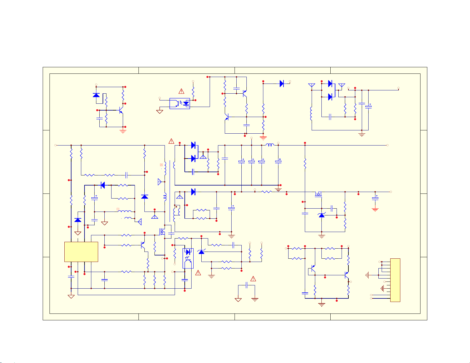
D
C
B
A
VPFC
IC1
LD7750
Z2
22V
104
C1A
TEST12
TEST13
OTP
TEST15
R16
R17
68R/1W
10K
R14
10K
1 2
7
8
FB CS GND
123
TEST16
TEST17
Z5
22V
TEST55
C9
104
R6
68R/1W
R13B
10R
TEST18
6
OUTVCCNCHV
Inverter
1 2
10uF/50V
C2
103/50V
4 5
D2
FR107
EC2
R4
68R/1W
TEST19
101
C1
R78
470R
1
R79
10K
C37
NC
ADJ
BKON
4
EC6
1000uF/25V
+12V
5VSB
100uF/16V
EC5
Inverter
+12V
5VSB
CN1
1
2
3
4
5
6
7
8
9
10
11
12
WJ6P2*2
D
C
B
A
带扣
1 2
R33
820R
TEST47
R34
10K
L3
FB
EC9
1000uF/25V
R21
3.9K*1%
321
Z4
+12V+12V
TEST44
E17
1
15V
3
12
D4A
FCH20100
T1L
T1J
10
V1
220uF/25V
TEST27
ADJ
TEST29TEST30
TEST26
R92A
3.9K
EC10
QS1
2 3
TEST28
1
CS1
104/50V
TEST39 TEST40 TEST41
R93
12K*1%
R94
NC
C7
104/50V
2 3
R95
7.5K*1%
R35
NC
Q4
1
4403
2 3
TEST42
R97
200K*1%
TL431
US1
C10
102/1KV
104/50V
CS2
1
TEST34
E11
R8
10R
TEST45
Inverter
2
R9
10R
TEST46
TEST35
RS1
11K
RS2
12K
VDD
R96
10K*1%
Q3
1
4403
DIM
2 3
R40
10K*1%
TEST51
104/0805
TEST50
R29
10R
TEST25
R22
10K
Q12
4401
3 2
104/0805/50V
C9B
C6
102
TEST32
TEST33
10K 1%
R19
150K 1%*
R19A
R30
3.9K
R31
220R
1
1
EC3
220uF/16V
C5
474
C38
TEST49
TEST38
TEST53
TEST23
D4
1
3
D3A
1 2
TEST31
8
R23
1K
1
2
4
3
102
C4
R24
1K
TEST52
1
2
E18
C8
102/1KV
SB260
10R
R26
10R
R25
U1
PC817
2
R28
10R
TEST37
2 3
TEST24
IC2
TL431
1
R80
680R/2W
TEST56
Q13
4401
3 2
TEST54
C3
472/400V
R15
12
4.7R
R13
4.7R
T1D
T1F
4
T1E
6
E14
5
R12
82R
R11
1
1K
R7
20R
100R
R5
R18
100K/2W
TEST11
D1
FR207
1 2
Q2
TEST20
12N60
Q1
4403
2 3
R1
1.5RR21.5R
FB
T1
EPC34
E15
TEST14
E9
1
R10
10K
BB
0.22R/2W
U2
4
3
PC817
T1K
2
11
1
12
L1
FB
E16
7
23
9
C3B
TEST36
R20
101/1KV
510R
TEST21
R3
12
FB
Q11
4403
2 3
1000uF/25V
Inverter
CY1
R32
220R
C39
104/0805
12
EC7
9
R27
11K*1%
TEST48
1 2
EC8
1000uF/25V
R26B
470R
+12V
102 Y1
TEST22
TEST43
1 2 34
Page 27

1
FL3
FILTER
4
TEST113
4
CON5
CON2
CON4
CON2
CON3
CON2
TEST107
D
1
2
C
1
2
B
1
2
A
321
T4
R83
15R
TEST84
TEST86
C40
222
R77A
15R
R77
15R
T4G
T4E
V+
T4C
EEL19
T4A
V+
TEST117
T2G
EEL19
T2E
V+
T2C
EEL19
T2A
R82
15R
7
5
3
1
T3
3 5 7
1
7
T2
5
TEST120
3
1
EEL19
98
988
9
T2H
EEL19
T2I
TEST93
TEST103
TEST111
TEST104
TEST112
C36
20PF/6KV
R74
C35
30K
681
C34
681
R73
30K
C32
20PF/6KV
C31
20PF/6KV
R70
C30
30K
681
C29
681
R69
30K
C28
20PF/6KV
C27
20PF/6KV
R66
C26
30K
681
C25
681
R63
30K
C24
20PF/6KV
TEST88
TEST95
R75
10K
D11
1
TEST90
2
1
VS
3
TEST91
LBAV70
TEST94
R72
10K
3
TEST92
TEST96
TEST98
TEST101
R71
10K
D10
1
TEST100
2
2
VS
3
TEST99
LBAV70
R68
10K
TEST102
1
TEST97
TEST105
CS
TEST115
TEST106
TEST114
R62
13K
R64
1.5K
1.5K
R65
2
1
3
R67
10K
D9
LBAV70
R61
10K
3
TEST110
2
VS
TEST109
2
TEST108
3
Title
Number RevisionSize
A4
Date: 18-Oct-2010 Sheet of
File: F:\
项目\MIP236-VT\PCB&SCH\0928\MIP236-VT-1.1(2010.09.29 ).dd bDrawn By:
R76
R59
10R
C23
102
TEST87
R54
10R
TEST74
Vds1
R60
10R
R55
10R
TEST85
C22
102
R81
15R
Vds2
Vds1
Vds2
Vds1
Vds2
15R
C33
222
TEST116
TEST118
TEST119
TEST121
TEST57
Inverter
R56
43K
C20
474
TEST122
2
VDD
EC11
D7
D5
R48NCCS
LBAV70
BAV70
3
1
12
TEST65
1
2
3
TEST64
D
VDD
TEST59
1
TEST60
R39
10K
Q5
2N7002
1000uF/25V
CS
23
23
Q8
1
2N7002
R52
1M
XX
TEST124
BKON
R38 20K
R37
C
100K
R36
15K
1
Q6
2N7002
C19
105
R47
2.4K
C15
105
23
TEST66
VS
TEST67
TEST68
B
C11
103
C12
103
R41
10K
TEST69
R42
100K
C13
223
BKONDIM
R58
150R
R57
51R
R53
100R
R51
51R
G1
8
VDD
7 10
6
CS4 CS2
5
CS3
4
VS
3
BF
2
DIM
1
IC3
OB3306
TEST81
1
3
D8
LBAV70
TEST82
2
TEST80
1
3
D6
LBAV70
2
TEST79
G2
9
GND
11
12
CS1
13
CMP
14
DRC
15
RT
16
RIENA
TEST70 TEST72
12
R50
R49
5.1K
430R
1
AOD454A
1
AOD454A
C16
471
TEST76
C14
472
TEST77TEST78
R43
120K
TEST73
TEST83
23
Q9
C21
474
23
Q7
C17
C18
103
472
R46
CS
3.6K
R45
3K
R44
43K
TEST61
TEST62
A
Q10
1
4401
Z1
5.6V
VDD
3 2
1 2
1 2 34
 Loading...