

Page 1
Disassembly of the LxxWD250
Page 2
Disassembly of the LxxWD250
• Use the following disassembly instructions and
you will not need to lay the unit down on it’s front.
Page 3
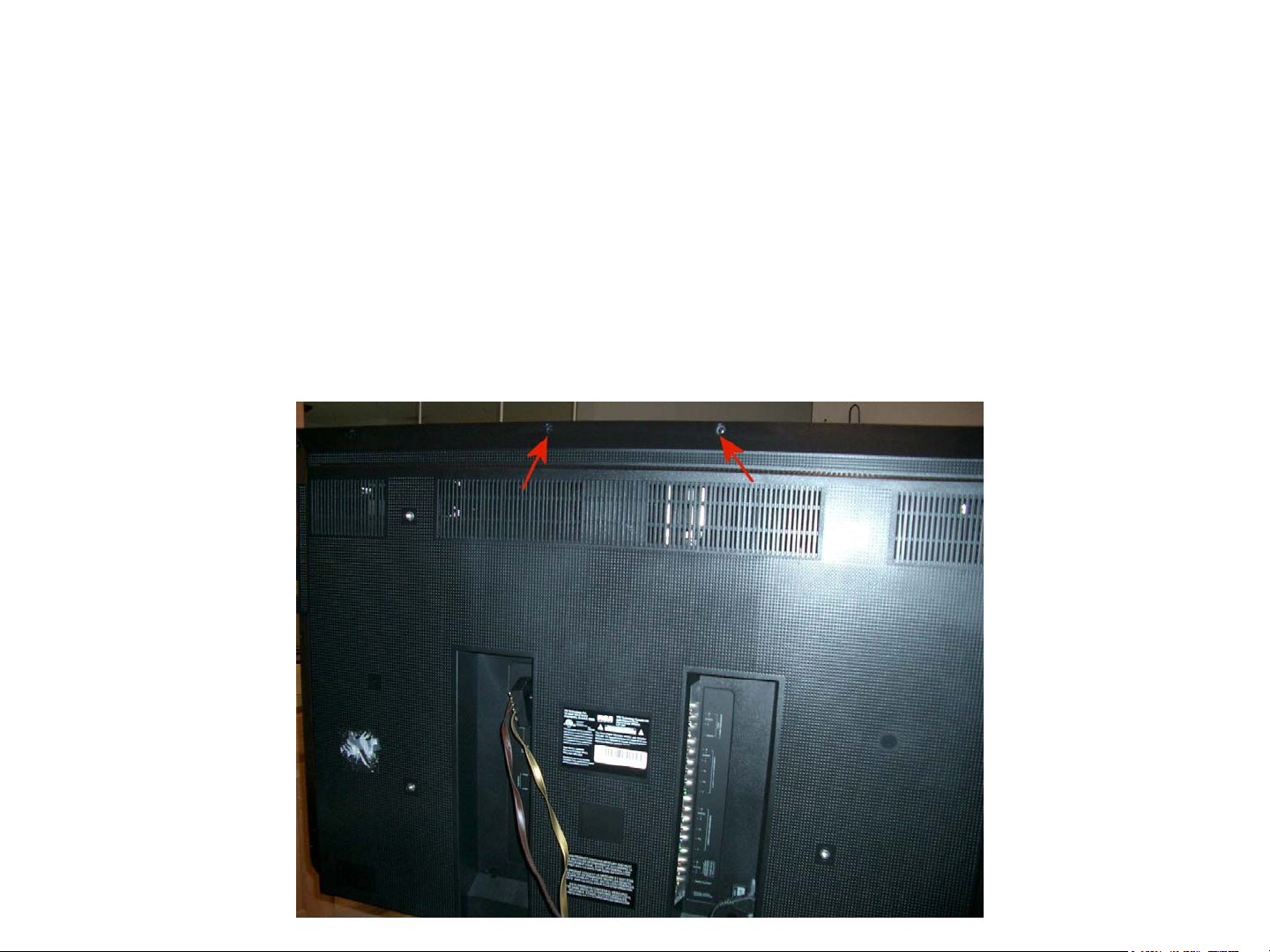
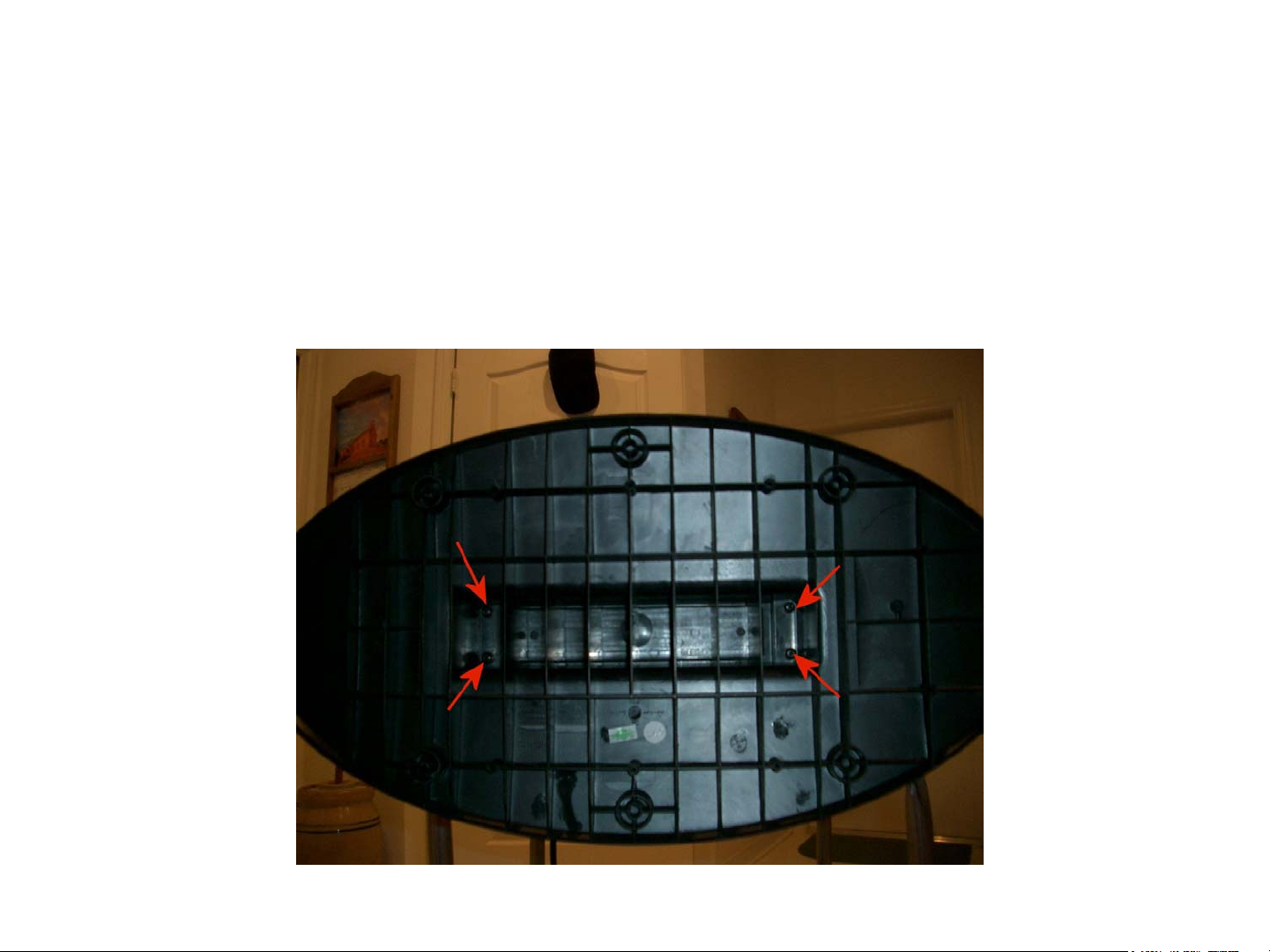
Disassembly of the LxxWD250
• Stand unit up right on work table.
• Remove all screws mark by an arrow. (8-14
depending on screen size)
Page 4
Disassembly of the LxxWD250
• Lay unit on back.
Page 5
Disassembly of the LxxWD250
• Remove screws and base. (4 screws)
Page 6
Disassembly of the LxxWD250
• From under base mounting plate remove 4
screws that hold mask (screen frame) in place.
• DO NOT remove large silver screws!
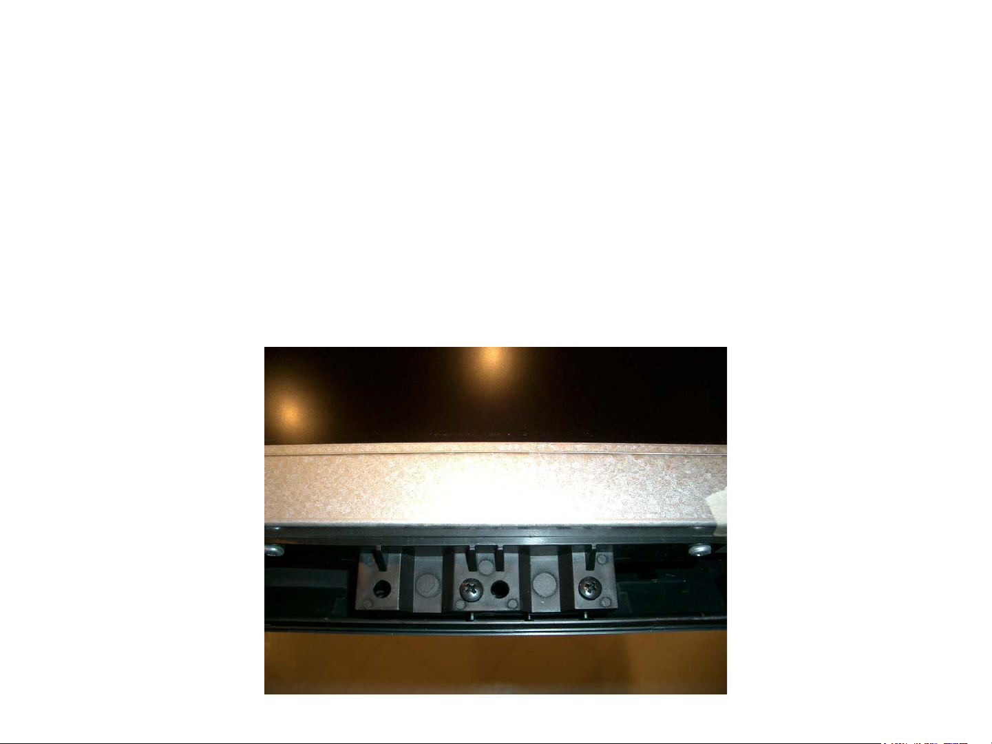
Page 7
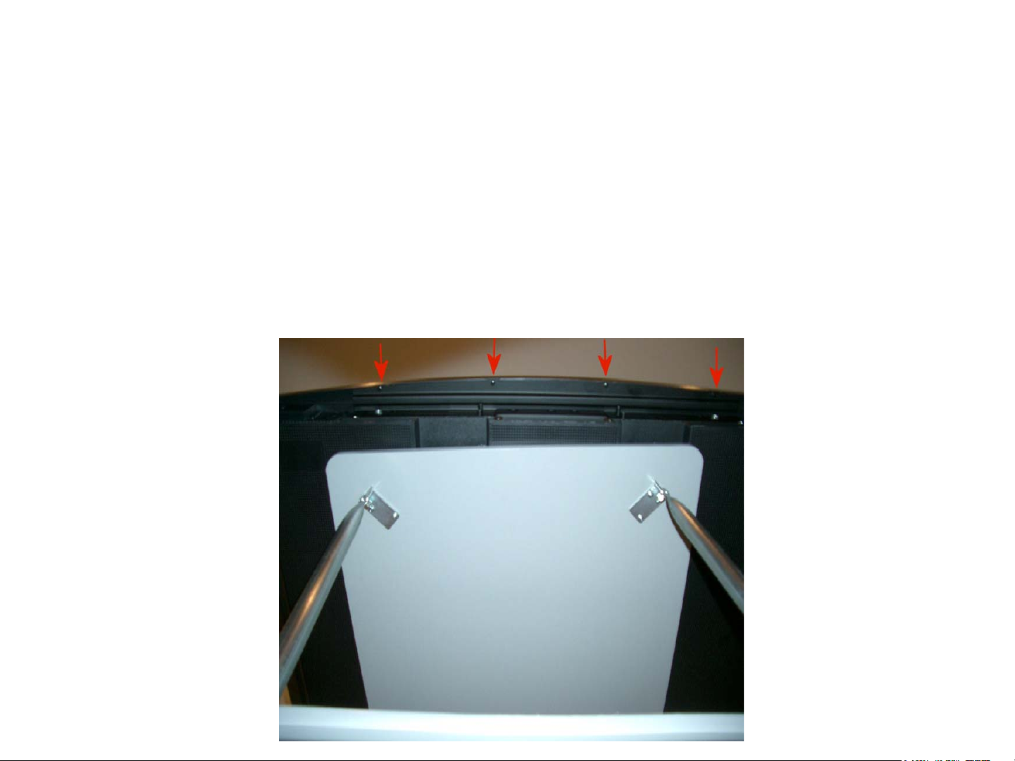
Disassembly of the LxxWD250
• Grasp bottom center of Mask (screen frame) and
gently, slowly lift up and forward.
Page 8
Disassembly of the LxxWD250
• Disconnect speaker wire connectors. (2 cables)
Pay attention to which wire goes to left and right
speakers.
Page 9
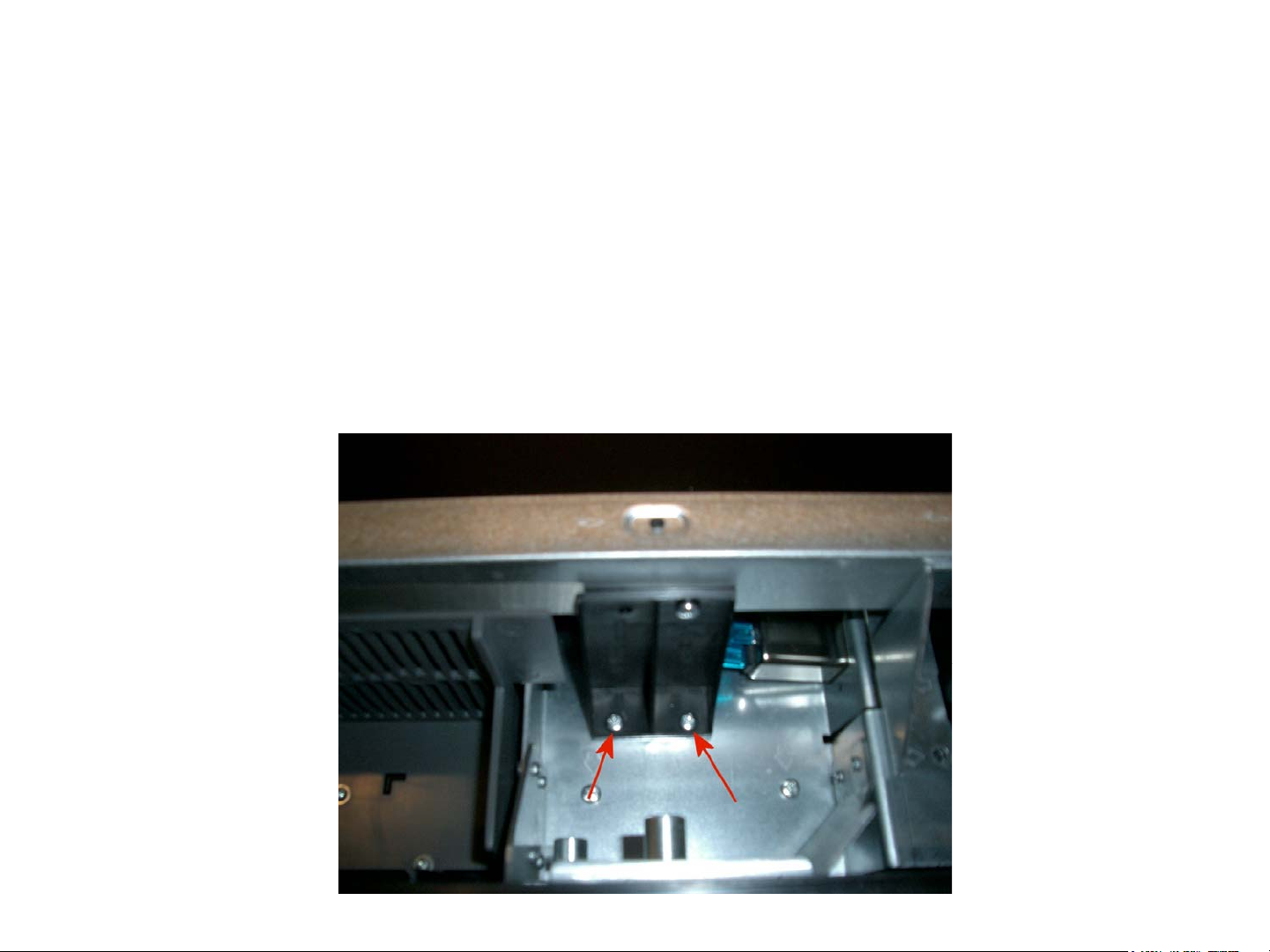
Disassembly of the LxxWD250
• Remove 2 screws from each display mount. 2
mounts on the left and the right side of display
assembly. (Top right mount shown below)
Page 10
Disassembly of the LxxWD250
• Remove 2 screws each from the two bottom
mounts of screen display assembly.
• DO NOT Remove any other screws from unit.
Page 11

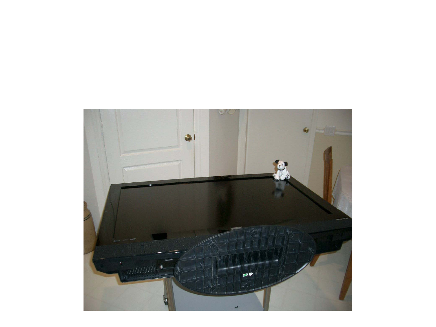
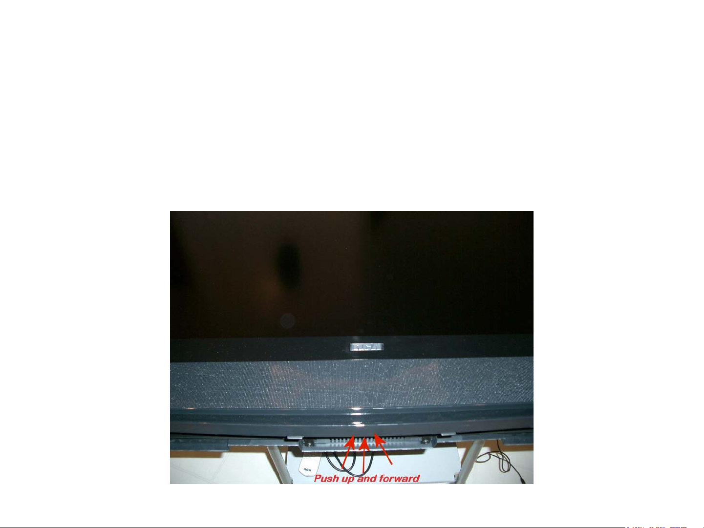
Disassembly of the LxxWD250
• Grasp bottom of display assembly and pull up
and forward. Assembly will hinge upwards.
• Do not pull up more than 12 to 24 inches.
Careful not to pull wires taught. You can pull
plugs from connectors!
Page 12

Disassembly of the LxxWD250
• Using a dowel rod or curtain rod that is 18 to 22
inches in length, ½ inch or larger diameter, prop
up display assembly as shown in picture below.
Page 13

Disassembly of the LxxWD250
Page 14

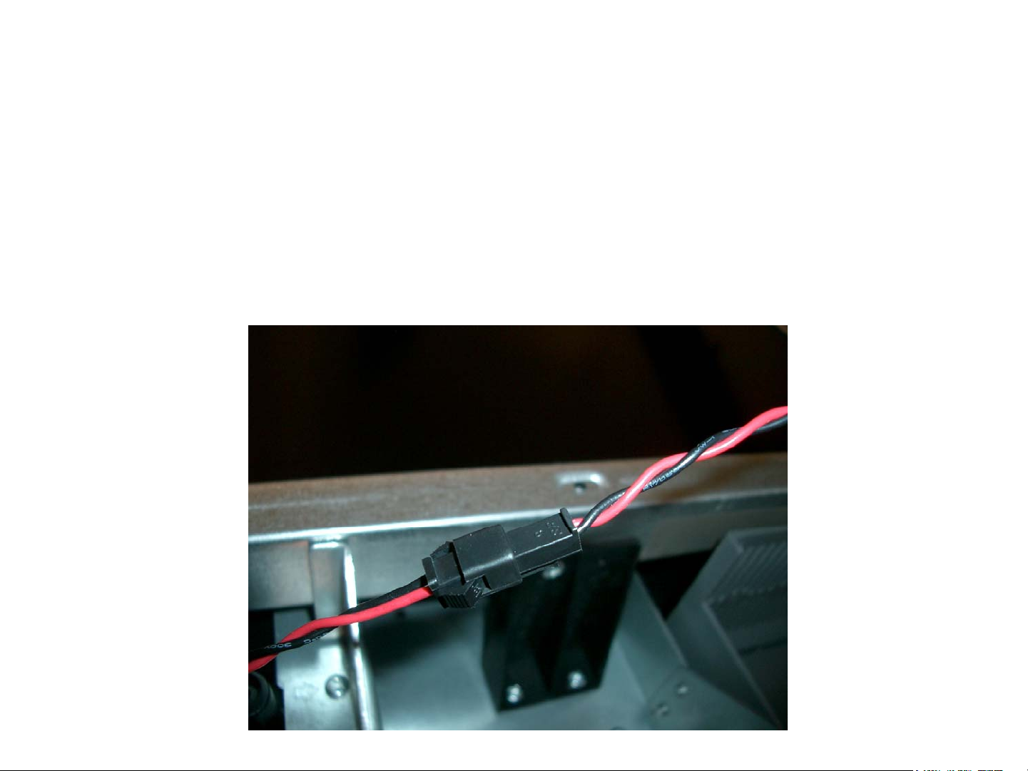
Disassembly of the LxxWD250
Careful not to pull cable too tight else plug will separate from connector!
Page 15

Page 16

P810
Alignments
Entering the Factory Service mode
Turn the instrument OFF. Then press the Vol - button on the
remote and Vol - on the keypad simultaneously. Hold the
buttons for approximately 10 seconds until the instrument
turns ON. Using the remote if you want to select an item,
press the Up (^) and Down (v) buttons. Adjust the setting
value using the Left (<) and Right (>) key. Press the Clear
button to return to the main menu after adjusting a value.
Press the Clear button or select Go Back the menu to exit
the Factory Service mode.
Clear RRT: Clears the Regional Ratings Table. Select OK to
clear the table.
Test Pattern
The Test Pattern menu will display either a multiple color
bar or a flat color screen. Each display will be visible for
approxitimately 5 seconds. Use the arrow up or down on the
remote to select Test Pattern from the menu. Then use the
OK button on the remote to enter the next menu. Select Go
Back to return to the previous menu.
Local Upgrades/Applications: Will search for software up
grades, then initiate the upgrade process.
Current Software Info: Displays the current software version
and the date of install.
Video Alignment
The Cut Off alignment is used to define the color
coordinates for low level luminance. The Whitepoint is
used to define the color coordinates for bright luminance
This alignment must be completed using Line Input
(CVBS).
Multiple Color: Select, then select OK to display multiple
bands of color.
Main Menu
The Main Menu includes the following features:
Dealer Service Menu: This is at the very top of the screen. It
contains the current software version loaded in the instrument.
Go Back: Returns to the previous menu.
Test Pattern: Menu will bring up color test screens.
Speaker Test: Press OK for a 5 second test tone.
Operating Hours: Displays the hours of operation
NVM Initialise: Clears the NVM. This function resets all
customer settings to a out of box condition. Press the OK
button to start the process.
Reset Operating Hours: Resets the operating hours to 0.
Current Software Info: Displays the current software
version.
Software Upgrade: Allows for software upgrades.
Single Color: Will bring up 2 options.
Manual: Select which color to display (Red, Green, Blue,
White and Black). Press the OK button on the remote to
display the pattern.
Software Upgrade
Software upgrades are installed by the use of a generic USB
device. Specific instructions related to software updates will
be released within the software data package.
1. Enter the Factory Service mode.
2. Select VIDEO from the menu, then select Normal from
the Color Temperature sub-menu.
NOTE: It is only necessary to perform the Cut Off and White
Point Alignments with the Color Temperature set to
the Normal position. The values for Cool and Warm
are interpolated based on the Normal settings.
3. Insert a grey test pattern with a 10 to 20 Nits luminance
level.
4. Using a Color TV Analyzer meaure the coordinates at
the center of the screen. Adjust Red Offset, B Offset and
Green Offset for x = 0.280 +/- 5%, y = 0.290 +/- 5%
5. Insert a 50IRE (or 150 nits) grey test pattern.
6. Using a Color TV Analyzer measure the coordinates at
the center of the screen. Adjust R Gain, G Gain and B
Gain for x = 0.280 +/- 5%, y = 0.290 +/- 5%.
NOTE: It may necessary to switch between the Cut Off and
White Point Alignments in order to achieve the
proper alignment.
Picture: Customer Picture Menu
Video Alignment: Video Alignemt Menu
Automatic: Select, then select OK to scroll through the
different color screens (Red, Green, Blue, White and Black).
Will continue to scroll through the patterns until the OK button
is press.
Page 2-1
8. Exit the Service Menu by press the Clear button on the
remote.
Page 2-2
Page 17

P810
Alignments
Brightness Alignment
1. Enter the Factory Service mode.
2. Select VIDEO from the menu, then select Brightness.
3. Insert a pluge test pattern thru RF with a 2% setup
background with a 0% and 4% bar.
4. Adjust the Brightness so that the 0% bar is invisible
with the 4% bar visible.
5. Exit the Factory Mode by pressing Clear on the remote.
Peak White Adjustment
The Peak White alignment must be completed to the
following standards.
1. Enter the Factory Service mode.
2. Select VIDEO from the menu, then select Peak White.
3. Input a test pattern with a 100% white centered pad on
a dark background.
4. Using a Color TV Analyzer measure the luminance
level (Y[nit]) of the white pad. Adjust with the Scaling
Contrast the Light Output Level (PW Level) for 400
Nits + 20%/- 10%.
Defective Pixel Specification
A pixel is defined as three elements or dots, one red, one
blue, and one green. Thus one bright pixel is three bright
adjacent dots. No bright pixels are allowed but 3 bright
dots are allowed subject to the following:
The bright dots must be viewable on normal program
material (not static test patterns) when viewed at a distance
of five feet from a point perpendicular to the center of the
screen at eye level. The panel is considered defective if
the pixels are viewable and they are within ¼” of another
bright dot.
Also, no more than eight dark dots, and no dark pixels
will be accepted when viewed under the same conditions.
Page 18

P810 BLOCK DIAGRAM
C om ponent Input 1
C om ponent Input 2
Re ar C inch
FA V
DS UB
VG A
ED ID
EEP R O M
L-R
ED ID
EE PR O M
L-R
HD MI
HD M I / ADC
TD A 9975
A nalog Fr on t E nd
PN X 3000
EDI D
EE PR O M
DDR
SD R A M
16M x 16
D ig ita l A /V In pu t LV D S
Flash
512K b
S tandby uP 80C 51
IR KB
PN X 2015
A udio
S erial A /V Input
TU N N E L
Processor
Flat P anel Display
Audio Am p
D igital-A n alog F ront E nd
TD 13660
AT S C, NTS C, QAM
O O B Tu ner
uP C 3200 G R
Ch annel Decoder
FD C FA T
NX T2003
Tu ne r
DE NC
IF
Monitor Out
PN X 8550
US B 1.1
T ran sp o rt S trea m
CI Co ntrol
STV 0701
POD
DDR
S DRAM
2x 8M x 16
E EPR OM
8K x 8
NA ND
EE PR OM
32M x 16
Page 19

P810 Base Exploded View
1
1
2
3
5
6
4
BRACKET FOOT
BASE
MACHINE SCREW
BASE PANEL
SCREW
FOOT PAD
2
3
4
5
6
Page 20

P810 Chassis Exploded View
20
27
25
23
29
22
3
17
18
14
15
4
16
30
2
24
9
1
8
26
21
ASM BRACKET
10
7
5
34
36/37
12
11
13
1
2
SCREW M/C B 4 X 8
LEFT BRACKET
3
4
SCREW M/C B 4 X 8
5
RIGHT BRACKET
6
SCREW M/C B 4 X 8
BRACKET
7
8
SCREW TRIANGLE M/C B 3X8
SCREW TRIANGLE M/C B 3X8
9
10
SCREW TRIANGLE M/C B 3X8
11
POWER BRACKET
12
SCREW TRIANGLE M/C B 3X8
13
SCREW TRIANGLE M/C B 3X8
14
BRACKET
15
SCREW TRIANGLE M/C B 3X8
16
BRACKET POWER SOCKET
SCREW B 4 X 15 AB
17
18
SCREW M/C F 3 X 10
TWIST TIE NY66
19
20
SCREW TRIANGLE M/C B 3X8
21
SPONGE
22
SPONGE
23
TERMINAL BAR
SCREEN COVER
24
25
SCREW TRIANGLE M/C B 3X8
26
SCREW TRIANGLE M/C B 3X8
27
SCREW TRIANGLE M/C B 3X8
SCREW TRIANGLE M/C B 3X8
29
30
SCREW TRIANGLE M/C B 3X8
34
SCREW TRIANGLE M/C B 3X8
36
SPACER SUPPORT
37
FIBER SINK
6
Page 21

P810 Front Cabinet Exploded View
1
11
2
8
7
6
3
4/5
9
1
SPONGE
SCREW S/T B 3 X 8 AB
2
3
SCREW S/T B 3 X 10 AB
4
SCREW S/T B 3 X 10 AB
SCREW S/T B 3 X 10 AB
5
10
6
FRONT CABINET
7
INLAY KEY
8
PUSH BUTTON
REAR AV COVER
9
10
LUCENCY BAR
SCREW S/T B 3 X 10 AB
11
Page 22

P810 Rear Cabinet Exploded View
4
6
3
3
4
5
5
6
REAR CABINET
MODEL PLATE
SCREW S/T B 4 X 15 AB
SCREW M/C B 4 X 8
Page 23

P810 INTERCONNECT DIAGRAM
1 GND 11 GLINK-IR-OUT
2 YPbPr2-Y 12 GLINK-TXD
3 GND 13 GLINK-RXD
4 YPbPr2-PB 14 A-PLOP
5 GND 15 P50
6 YPrPb2-PR 16 SCL-MM
7 GND 17 SDA-MM
8 SPI-1 18 LED2
9 HSYNC-HIRATE 19 LIGHT-SENSOR
10 SPI-OUT 20 COM-SND
1 GND 21 +5V2-STBY
2 AV2/AV4_G-Y 22 CVBS-TER-OUT
3 GND 23 GND
4 AV2/AV4_B-PB 24 AUDIO-IN1-L
5 AV2/AV4_R-PR 25 AUDIO-IN1-R
6 GND 26 GND
7 +8V6-SW 27 AUDIO-IN2-L
8 GND 28 AUDIO -IN2-R
9 Y-CVBS-MON-OU 29 GND
10 GND 30 FRONT-Y-CVBS
11 N/C 31 GND
12 GND 32 FRONT-C
13 AUDIO-OUT2-L 33 GND
14 AUDIO-OUT2-R 34 AUDIO-IN3-L
15 GND 35 AUDIO-IN3-R
16 AUDIO-HDPH-L 36 GND
17 AUDIO-HDPH-R 37 AUDIO-IN4-L
18 GND 38 AUDIO-IN4-R
19 AV1-CVBS 39 GND
20 GND 40 GND
RIGHT
SPEAKER
LEFT
SPEAKER
BA003
BA004
BA001
Audio
Amp
Board
BA002
1
BV020
1
+12VDD
PGND
AM & DC
Board
(WD22/WD250)
AMP_L_IN
GND_BTL
AMP_R_IN
AGND
AMUTE
A-PLOP
1
20
Power Interface Board
BP700
1
5V
GND
8V6
12V
1
1
1D40 1M46
1M52
Digital Board
1E62
BP600
1M03
GND
Main
+12VDD
1
PGND
AC
IN
CON1
Power
Board
GND
5.2V_STBY
1
GND
LIGHT-ON-OUT
1
BACKLIGHT-CONTROL
1
CON3
12V
GND
P-ON
CN2
GND
1
+24V
CON4
+24V
GND
CN1
LCD Panel
AV Board
BV500
FAV_L
AGND
FRONT_C
Board
AGND
FAV_R
BV500
1
FAV_CVBS
AGND
1
FAV
BQ002
HP_L
BA202
BU001
BV010
1
HP_R
AGND
1
VDISP
1
VDISP
3
VDISP
1
1E40
1G50
40
5
CTRIL-DISP1
7
CTRIL-DISP3
9
TXPNXA+
11
TXAC+
13
TXPNXB-
15
GND
17
TXPNXC+
19
TXPNXCLK-
21
GND
23
TXPNXD+
25
TXPNXE-
27
GND
29
SDA_I2C4_DISP
31
SCL_I2C4_DISP
LED_1
1
VBUS
USB-
1
USB+
AGND
1M65
1E42
AGND
1
LED_2
GND
RC
+5V2_STBY
1
Keyboard
BK001
VDISP
VDISP
VDISP
CTRIL-DISP2
CTRIL-DISP4
TXPNXA-
GND
TXPNXB+
TXPNXC-
GND
TXPNXCLK+
TXPNXD-
GND
TXPNXE+
GND
BK002
2
4
6
8
10
12
14
16
18
20
22
24
26
28
30
32
GND
1
IR_1
5V
G_LED
R_LED
1
IR
Board
BK102(P1)
KEYBOARD
GND
P2 (WD22/250)
Page 24

P810 CONNECTOR LOCATION GUIDE DIAGRAM
A u d io A m p lifie r B o a rd
PO D
S tereo Ja c k
Ou t
SP DIF
Pow er Interface
Mon itor OutCo mpon ent 1Co mp onent 2Re ar A/V
Po we r
Int e r f ac e
Pa ne l
Inv erter
VG A
Pow er S upply
Mainboa rd
HDMI with L /R
I/O B o ard
US B
HDMI
LV DS
NT S C /AT S C
Tu ner
FAV
S
Video
HP
US B
Page 25

Dead Set
Troubleshooting
Start
Measure Pin 3
of CON 2 for
+5Vdc.
+5V present?
YES
Press Power
Switch, monitor
CON 3 Pin 7 for
+5V
+5V present?
YES
Check CON 3
Pin 1 for +12V
Pins 5/6 for +24V
NO
Suspect Main
SMPS
NO
BK001
Function DC Voltage
Power 2.7
Channel + 1.4
Channel - 0.84
Volume + 2.2
Volume - 1.8
Menu 2.5
No Key Press 2.9
Using the chart to the right,
verify the correct voltage on
pin 6 of BK001 for each FPA key
YES
press.
Voltages
Correct?
NO
Suspect Main
SMPS
NO
Monitor BP700 for the following
Voltages
Correct?
YES
voltages.
Pins 1/2 for +5V
Pin 4 for +8.6V
Pins 6/7 for +12V
Voltage
Correct?
YES
Suspect Digital
Board
NO
Troubleshoot
Digital Board
Suspect Power
Interface Board
Troubleshoot
FPA and Key
scan circuit
Page 26

Video OK
No Audio
Start
With the set
Powered On,
check BA001
Pin 1 for +12V
Voltage
present?
YES
Check BA002
Pins 1 and 3 for
audio signal
Signal
present?
YES
Check BA002
Pins 5 for 0V
Pin 6 for-0.2V
NO
NO
Suspect Main
SMPS Board
Suspect Digital
Board
Suspect Speakers
YES
Voltages
present?
YES
Check for Signal
on BA003 and
BA004
Signal
present?
NO
NO
Suspect Digital
Board
Suspect Audio Amp
Board
Check the Sound
Menu. Make sure
Internal Speakers
is checked.
Page 27

Sound OK
No Video
Start
With the set
Powered On,
check 1M03
Pin 1 for +8.5V
Pin 3 for +5V
All voltages
present?
YES
Check CON 3
Pins 5/6 for +24V
Voltages
present?
YES
Check signals
on 1G50
NO
NO
Suspect Digital
Board
Suspect Main
SMPS Board
Signals
present?
YES
Suspect LCD
Panel
NO
Suspect Digital
Board
Page 28

P810
VOLTAGE CHARTS
AUDIO AMP BOARD
AV BOARD
100AB 200AB 300AB 400AB
#NIP
CD
STLOV
#NIP
CD
STLOV
#NIP
CD
STLOV
#NIP
17.11 16.5 19.5 10.6
20.0
20.0 29.5 20.6
35.5
40.0
510.0
622.0-
200QB 010VB 020VB 005VB
CD
STLOV
#NIP
CD
STLOV
#NIP
CD
STLOV
#NIP
CD
STLOV
#NIP
CD
STLOV
#NIP
CD
STLOV
10.0 10.0 620.0 10.0 10.0
20.0
30.0
24.1 720.0 22.1 20.0
30.0 820.0 30.0 30.0
44.1 920.0 42.1 40.0
54.1 032.3 50.0 50.0
60.0 130.0 62.1 60.0
75.8 230.0 70.0
80.0 330.0 80.0
95.4 430.0 93.3
010.0 530.0 010.0
119.0 630.0 110.0
210.0 730.0 213.3
316.3 830.0 313.2
416.3 930.0 4122.0-
510.0 040.0 512.3
610.0 610.0
710.0 710.0
810.0 815.4
910.0 9114.0
020.0 022.3
129.4
220.0
320.0
Page 5-1
420.0
520.0
Page 5-1
Page 29

P810
VOLTAGE CHARTS
FRONT AV BOARD
202AB 100UB 005VB
#NIP
CD
STLOV
#NIP
CD
STLOV
10.0 11.5 10.0
20.0
30.0
20.0 20.0
30.0 30.0
40.0 40.0
50.0 50.0
#NIP
60.0
70.0
IR BOARD
201KB
NUR
CD
STLOV
#NIP
CD
STLOV
#NIP
201KB
FFO
CD
STLOV
10.0 10.0
23.3
39.4
48.1
512.0
23.3
39.4
48.1
50.2
LCD PANEL
#NIP
10.42 10.42 181.0
20.42
30.42
40.42 40.42
50.42 50.0
1NC 2NC
CD
STLOV
#NIP
20.42 22.0
30.42
1NC
)THGILKCAB(
CD
STLOV
#NIP
CD
STLOV
60.0 60.0
70.0 70.0
80.0 80.0
KEY BOARD
100KB
#NIP
CD
12.2 REWOP7.2 10.0 10.0
25.4
30.0
43.3
59.4
69.2
90.0 90.0
010.0 010.0
114.8
100KB
6NIP
STLOV
NOITCNUF
CD
STLOV
200KB
NUR
#NIP
CD
STLOV
200KB
211.5
FFO
#NIP
CD
STLOV
+HC4.1 23.3 23.3
-HC48.0 39.4 39.4
+LOV2.2 48.1 48.1
-LOV8.1 512.0 50.2
UNEM5.2
70.0
Page 5-2
Page 5-2
Page 30

P810
VOLTAGE CHARTS
MAIN BOARD
04D1 05G1 04E1 24E1
#NIP
CD
STLOV
#NIP
CD
STLOV
#NIP
CD
STLOV
#NIP
CD
STLOV
#NIP
CD
STLOV
#NIP
CD
STLOV
24E1
6NIP
NOITCNUF
CD
STLOV
26E1 30M1 64M1 25M1 56M1
#NIP
CD
STLOV
#NIP
CD
STLOV
#NIP
CD
STLOV
#NIP
CD
STLOV
#NIP
1CN 19.4 620.0 10.0 620.0 12.2 REWOP7.2 10.0 14.8 10.0 16.5 11.5
2CN
30.0
4CN
50.0
6CN
29.4 72CN 24.1 720.0 25.4 +HC4.1 22.1 2CN 20.0 20.0 20.0
39.4 82CN 30.0 820.0 30.0 -HC48.0 30.0 31.5 35.8 35.5 30.0
49.4 920.0 44.1 920.0 43.3 +LOV2.2 42.1 40.0 46.11 40.0 40.0
59.4 03CN 54.1 032.3 59.4 -LOV8.1 50.0 5CN 51.5 510.0 50.0
6CN 13CN 60.0 130.0 69.2 UNEM5.2 62.1 6CN 60.0 622.0-
71.5 70.0 230.0 75.8 230.0 70.0 70.0 78.4 79.4
81.5 80.0 80.0 330.0 80.0 8CN 8CN
91.5 90.0 95.4 430.0 93.3 9CN 96.11
010.0 010.0 010.0 530.0 010.0 01CN 01CN
CD
STLOV
11CN 110.0 119.0 630.0 110.0 116.11
21CN 212.1 210.0 730.0 213.3
312.1 316.3 830.0 313.2
410.0 416.3 930.0 4122.0-
513.1 510.0 040.0 512.3
612.1 610.0 610.0
710.0 710.0 710.0
813.1 810.0 815.4
911.1 910.0 9114.0
020.0 020.0 022.3
122.1 129.4
222.1 220.0
320.0 320.0
423.1 420.0
522.1 520.0
Page 5-3
Page 5-3
Page 31

P810
VOLTAGE CHARTS
MAIN SMPS BOARD
006PB 007PB
#NIP
CA
STLOV
17.11 11.5
20.0
#NIP
21.5
30.0
45.8
50.0
67.11
77.11
POWER INTERFACE BOARD
1NOC
)SNIPSSORCA(
CD
STLOV
#NIP
CA
STLOV
2NOC 3NOC
#NIP
CD
STLOV
#NIP
CD
STLOV
10.121 1CN 19.11
20.121
20.0 20.0
39.4 30.0
4CN 40.0
50.42
60.42
78.4
Page 5-4
Page 5-4
Page 32

P810
WAVEFORMS
BA003 Pin 1 - Audio Amp Board BA004 Pin 1 - Audio Amp Board BV010 Pin 9 - AV Board
1E40 Pin 9 - Main Board
BV010 Pin 14 - AV Board
1E40 Pin 14 - Main Board
BV020 Pin 10 - AV Board
1E62 Pin 10 - Main Board
1G50 Pin 7 - Main Board 1G50 Pin 8 - Main Board
BV010 Pin 13 - AV Board
1E40 Pin 13 - Main Board
1G50 Pin 9 - Main Board
1G50 Pin 10 - Main Board 1G50 Pin 11 - Main Board 1G50 Pin 12 - Main Board
Page 5-1Page 5 - 1
Page 33

P810
WAVEFORMS
1G50 Pin 13 - Main Board 1G50 Pin 15 - Main Board 1G50 Pin 16 - Main Board
1G50 Pin 19 - Main Board 1G50 Pin 21 - Main Board 1G50 Pin 22 - Main Board
1G50 Pin 18 - Main Board
1G50 Pin 24 - Main Board
1G50 Pin 25 - Main Board CN3 - CN10 Pin 1 LCD Panel CN3 - CN10 Pin 2 LCD Panel
Page 5-2Page 5 - 2
 Loading...