RCA CTC203 Diagram

THOMSON TECHNICAL TRAINING
THOMSON TECHNICAL TRAINING
1999 ctc203 TRAINING
FOREWORD
This publication is intended to aid the technician in servicing the CTC203 television
chassis. It will explain the theory of operation, highlighting new and different circuits
associated with the digitally controlled chassis. The manual covers power supplies,
horizontal and vertical deflection, tuner, video signal processing, and audio signal
processing theory of operation along with practical troubleshooting tips and suggestions.
It is designed to assist the technician to become more familiar with chassis operation,
increase confidence and improve overall efficiency in servicing the product.
Note: This publication is intended to be used only as a training aid. It is not meant to
replace service data. TCE Electronic Service Information for these instruments contains
specific information about parts, safety and alignment procedures and must be consulted
before performing any service. The information in this manual is as accurate as possible
at the time of publication. Circuit designs and drawings are subject to change without
notice.
SAFETY INFORMATION CAUTION
Safety information is contained in the appropriate Thomson Consumer Electronics Service
Data. All product safety requirements must be complied with prior to returning the
instrument to the consumer. Servicers who defeat safety features or fail to perform safety
checks may be liable for any resulting damages and may expose themselves and others to
possible injury.
All integrated circuits, all surface mounted devices, and many other
semiconductors are electrostatically sensitive and therefore require
special handling techniques.
dbx® is a registered trademark of Carillon Electronics Corporation.
DirecTV® is a registered trademark of DirecTV, Inc., a unit of Hughes Electronics Corp.
Guide Plus+® is a registered trademark of Gemstar Development Corporation.
SRS®, the SRS symbol and Sound Retrieval System® are registered trademarks
of SRS Labs, Inc.
First Edition 9929 - First Printing
Copyright 1999 Thomson Consumer Electronics, Inc.
Trademark(s)® Registered Marca(s) Registrada(s)
Printed in U.S.A.
Prepared by
Thomson Consumer Electronics, Inc.
Technical Training Department
PO Box 1976
Indianapolis, Indiana 46206 U.S.A.
®

Contents
Chassis Description ............................................................................................................ 5
CRK76 Remote Control ............................................................................................................................... 9
Power Supply Overview .................................................................................................. 10
Standby Supply Overview ........................................................................................................................... 12
Digital Latches ............................................................................................................................................ 13
Control Latch Review ................................................................................................................................14
Latch Circuit ............................................................................................................................................... 15
Main Supply Block Diagram .......................................................................................... 16
AC Input and Degaussing ......................................................................................................................... 17
Main Supply Operation .............................................................................................................................. 19
Run Supplies ............................................................................................................................................... 27
Scan Derived Supplies ............................................................................................................................... 28
Deflection Overview ......................................................................................................... 30
Horizontal Output ...................................................................................................................................... 34
XRP ............................................................................................................................................................. 40
Horizontal Scan Derived Supply Generation ........................................................................................... 41
Vertical Scan Overview .............................................................................................................................. 42
System Control ................................................................................................................. 50
T4-Chip Power Control .............................................................................................................................. 57
Main Power Supply On/Off Control ......................................................................................................... 57
Batten Down the Hatches .......................................................................................................................... 58
V-Chip ......................................................................................................................................................... 67
Service Menu .............................................................................................................................................. 69
Error Codes .................................................................................................................... ............................72
Tuner.................................................................................................................................. 76
Instruments with GEMSTAR.................................................................................................................... 86
IF Circuit ........................................................................................................................... 92
F2PIP ................................................................................................................................. 94
Analog Switches .........................................................................................................................................96
Main Signal Processing.............................................................................................................................96
Burst Lock Clock........................................................................................................................................96
Video Input Switching ................................................................................................................................ 98

Video Processing ............................................................................................................. 100
CRT Drivers .................................................................................................................... 108
CTC203 Video Module .................................................................................................. 112
T4-Chip U12101 ............................................................................................................. 114
T-Chip Overview ....................................................................................................................................... 114
CRT Management.......................................................................................................... 116
Deflection Processing .............................................................................................................................. 116
Video Processing ...................................................................................................................................... 116
Analog Comb Module.................................................................................................... 118
Composite Video Switch ........................................................................................................................... 119
Analog Comb............................................................................................................................................ 119
S-Video Switch..........................................................................................................................................120
Input Jacks ............................................................................................................................................... 120
Output Jacks.............................................................................................................................................121
Power Supplies ......................................................................................................................................... 121
Audio................................................................................................................................ 122
Stereo/SAP Decoder ................................................................................................................................. 123
Stereo/SAP Switch .................................................................................................................................... 124
DBX...........................................................................................................................................................124
GEMSTAR ...................................................................................................................... 128
Operation ..................................................................................................................................................131
Diagnostic Test .........................................................................................................................................134
Troubleshooting ....................................................................................................................................... 136
Chipper Check™ Overview.......................................................................................... 138
Chipper Check™ Hardware....................................................................................................................139
Chipper Check™ Software ...................................................................................................................... 140
“Dead Set” Troubleshooting with Chipper Check™.............................................................................140
Further Reading ....................................................................................................................................... 145

4 Overview
INTRODUCTION
The CTC203 series chassis is Thomson Consumer Electronics latest core-line chassis. Consumer
operation and majority of features of the CTC203 series chassis are very similar to previous ProScan,
RCA and GE chassis. Menu structures will be recognizable to any previous TCE product user.
Although there are differences, the component designations on the CTC203 series chassis are similar
to designations on previous chassis. Most components are labeled on the circuit board. To save space
the first numbers from the schematic may be dropped off. Q14100 may become Q100 or Q4100.
However, it will probably be located in the 14000 series component area. In TCE Service Literature,
2 number components (R16) are generally located on the top of the circuit board, while 3 number
components (C523) are located on the bottom of the chassis.
It is important for the technician to understand the difference between switching transistors and
amplifiers. When switching transistors are "On", they have a very low emitter-collector voltage drop,
typically 0.12.1 volts. Transistor amplifiers are normally biased "On" at all times and while the
base-emitter voltage drop will be similar, (very close to 0.6 volts), the emitter-collector voltage drop
can be from around 1 volt up to the power supply voltage.
Although this Training Manual makes every effort to follow the service data template for component
location and identification, always consult the Basic Service Data (ESI) for up-to-date information.
The component type (transistor, resistor, capacitor...etc.) is designated by the way the component is
labeled in both Training and Service Data material.
CTC203 training material will include nomenclature that differs somewhat from previous manuals.
To designate individual pin assignments of an IC, the following will be shown;
U13101-5 designates IC U13101, pin 5.
Q14608-B indicates the base lead of transistor device Q14608.
Q14601-G indicates the gate of MOSFET device Q14601.
Power supply voltages and labels will be used whenever possible. +5Vr identifies the positive 5 volt
run supply. There are various classes of power supply indicators for the CTC203. They should be
self-explanatory to experienced technicians, but may differ slightly from designation used in TCE
Electronic Service Data. The common designations are:
l s - Standby
l r - Run
l Reg B+, which can be standby or run
l t - Tuner
Pay attention to which power supply is being referred to and confusion will be avoided. A standby
supply may also provide run current.
The CTC203 uses "Hot" and "Cold" grounds. Training material and service data will continue to
differentiate between the two using for hot ground and for cold. Always use an isolation
transformer when performing service on the CTC203 chassis.

Overview 5
Chassis Description
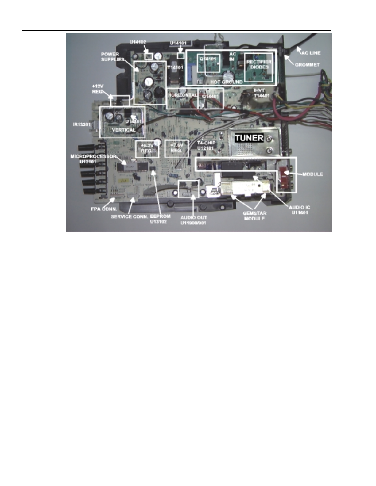
The CTC203 chassis will be used in a variety of models and screen sizes. Important additions include
a Gemstar Program Guide (Guide Plus+), V-Chip, on-board tuner, and a system control section that
can be connected to Chipper Check. It also has a number of chassis configurations that give the
chassis comb filter and S-Video capabilities. Active pincushion can also be switched in and out to
accommodate large picture tubes.
While the CTC203 is versatile, most major circuits are not new, but refinements of existing designs
modified to work together in the CTC203 chassis. For example, the switch mode power supply is
very similar to that of Thomsons MM101 chassis, the tuner section is close to the CTC175/6/7
chassis family, and system control will look and operate much like the CTC197 chassis. Keep in
mind there will be differences in symbol numbers and values of some components will change, but the
basic design is the same.
The CTC203 is expected to be a "workhorse" chassis, possibly replacing all CTC176/177/186/187
product. A commercial version (to support hospital, lodging, and educational markets) is also
planned.
6 Overview
Figure 1-1, CTC203 Chassis Layout
This CTC203 Technical Training Manual will break the chassis into several major
areas. Those areas are:
Main Power Supply
Scan Generated Power Supply
Horizontal Deflection
Vertical Deflection
System Control
Tuner
IF
F2PIP
Following the main discussions are several appendices which include pinouts of the
major IC's, overall block diagrams of System Control, Video Switching and Audio
Switching, a glossary of new and old terms used with the CTC203 and TCE chassis
in general and circuit board/component interconnect diagrams.
Video Module
Video Processing
Analog Comb Filter
CRT Management
Audio
GEMSTAR
Chipper Check
Overview 7
VIDEO
VCR
CONTROL
AUDIO
RL/MONO
IN
RL/MONO
OUT
S-VIDEO
F
S
CABLE/
ANTENNA
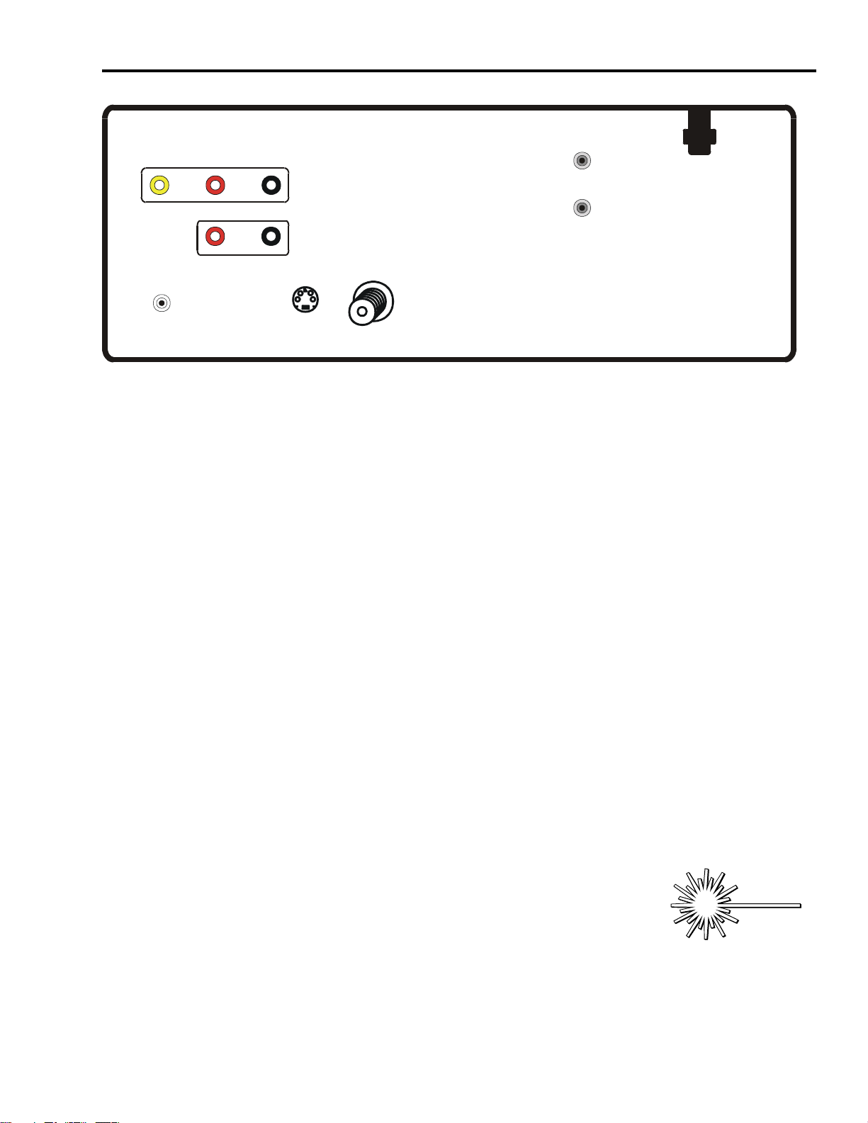
Figure 1-2, CTC203 Rear Panel
Rear Jack Panel
The CTC203 rear jack panel consists of three versions. One, shown above has
audio/video input and audio output jacks (5J). One has only audio/video inputs (3J)
and another has no audio/video input or output jacks (0J). All models have an RF
cable/antenna connecter and the VCR Control connection.
AC
LINE
CORD
The VCR Control connector enables the Guide Plus software to control a VCR or
Cable Box to either automatically tune to the selected Guide Plus channel or begin
recording a show selected in the Guide Plus menu.
Five jack (5J) models also have an S-Video input. If an active S-Video signal is
detected, the video input will automatically switch to the S-Video source.
The screen and focus adjustments are accessible from the rear panel without removing
the back of the set.
The Guide Plus+ software has a special learning/demo mode available to the
consumer. Most sets contain a pin inserted into the VCR CONTROL jack on
the rear panel of the set automatically enabling this mode. The pin activates
the mode every time the set is turned on. Although the set immediately
enters the demo mode it can be taken out via on-screen menu selection.
However, as long as the pin is the rear panel jack, the set will not receive channels
above VHF 13 whether the demo mode is active or inactive. The set must be
turned off, the pin removed and the set turned back on for normal operation to
return.
TECH
TIP
8 Overview
CH CTRL
SAT-CABLE
LED
SOUND
WHO-INPUT
SWAP
PIP
CH CTRL
RESET
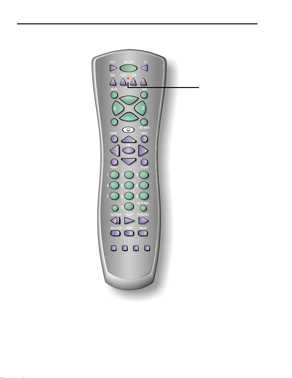
Figure 1-3, CRK76E1 Remote Control

CRK76 Remote Control
Although similar to previous remote controls, the CRK76 remote for the CTC203 has a
few added capabilities. Carried over are the "navigation" buttons located in the middle
of the remote. Instead of using "Channel Up", "Channel Down", "Volume Up" and
"Volume Down" to navigate through the on screen menu structure, these navigation
buttons will be used. The user will point using these buttons, then press "OK" to select
the desired instruction. They are also essential to the use of the Guide Plus+ menu
system.
The CRK76 series used in the CTC203 is also a "universal" remote capable of controlling
current equipment such as VCR's, Cable Boxes, and Satellite Receivers from most
major consumer electronics manufacturers. In addition, the remote may be programmed
to control RCA and RCA Dimensia audio equipment and RCA, GE and PROSCAN
DVD players.
Remote Control Operation
Normal remote functions will not be discussed. These functions have not changed over
the last several remote control models. The following text explains new buttons and
their functions.
Overview 9
LED: Indicates the remote is in "Learning" mode when programming the remote to be
used with other equipment.
SOUND: With one press brings the user directly to the audio processor menu.
Guide: Accesses the Guide Plus+ menu. When the remote is programmed to control
the SAT-CABLE equipment, accesses any available on-screen menus for those devices.
GO BACK: Returns the user to the previous channel selection, or if in MENU, returns
to the previous menu selection.
WHO-INPUT: Toggles through all available input sources.
SAT-CABLE: Places the remote in control of a compatible satellite receiver or cable
box. If Auto-tuning is enabled, also will turn on the TV and select the correct input to
display.
Some buttons and functions are not available on every model equipped with a CTC203
chassis. For instance, on models without PIP, the bottom four buttons on the remote
will not be present. Some models of the remote do not include back lighting and on
some models only the volume and channel buttons illuminate. Always consult the
latest ESI for the correct remote part number for a particular chassis prior to ordering
a replacement.

10 Power Supply
SERVICING
PRECAUTION!
Variable
IsoTap
AC Vol tag e Out
with 120VACIn
Monitor
ADD
Most ground connections on the CTC203 series chassis are
cold, ( ), indicating they are isolated from the AC line.
However, there are many "Hot" connections, ( ), meaning
direct connection to the AC line. The AC input and primary
side of the power supply circuitry are examples.
Always use an isolation transformer
and consult service data when performing service on this
chassis and other chassis in this family!
Power Supply Overview
There are three power supplies providing power to the CTC203. All derive power
from Raw B+ and/or Regulated B+. They are:
•Standby
•Run (Switched)
•Scan Derived (High Voltages)
Due to higher power requirements of the CTC203, the power supply takes a new
approach to meet the higher loads. Primarily, the main supply operates in "forward"
conduction mode, delivering power to the secondary transformer windings during
power transistor "on" time when the magnetic fields are expanding, rather than
during "off" time when the fields are collapsing.
All standby supplies also ramp up to supply the current demands of the chassis
during run operation. Derivations of the main supply also provide current for the
scan derived and the switched supplies.
There are three modes of operation for the main supply but only two for the switched
and scan derived supplies. They are:
•Standby
•Data Acquisition
•Run
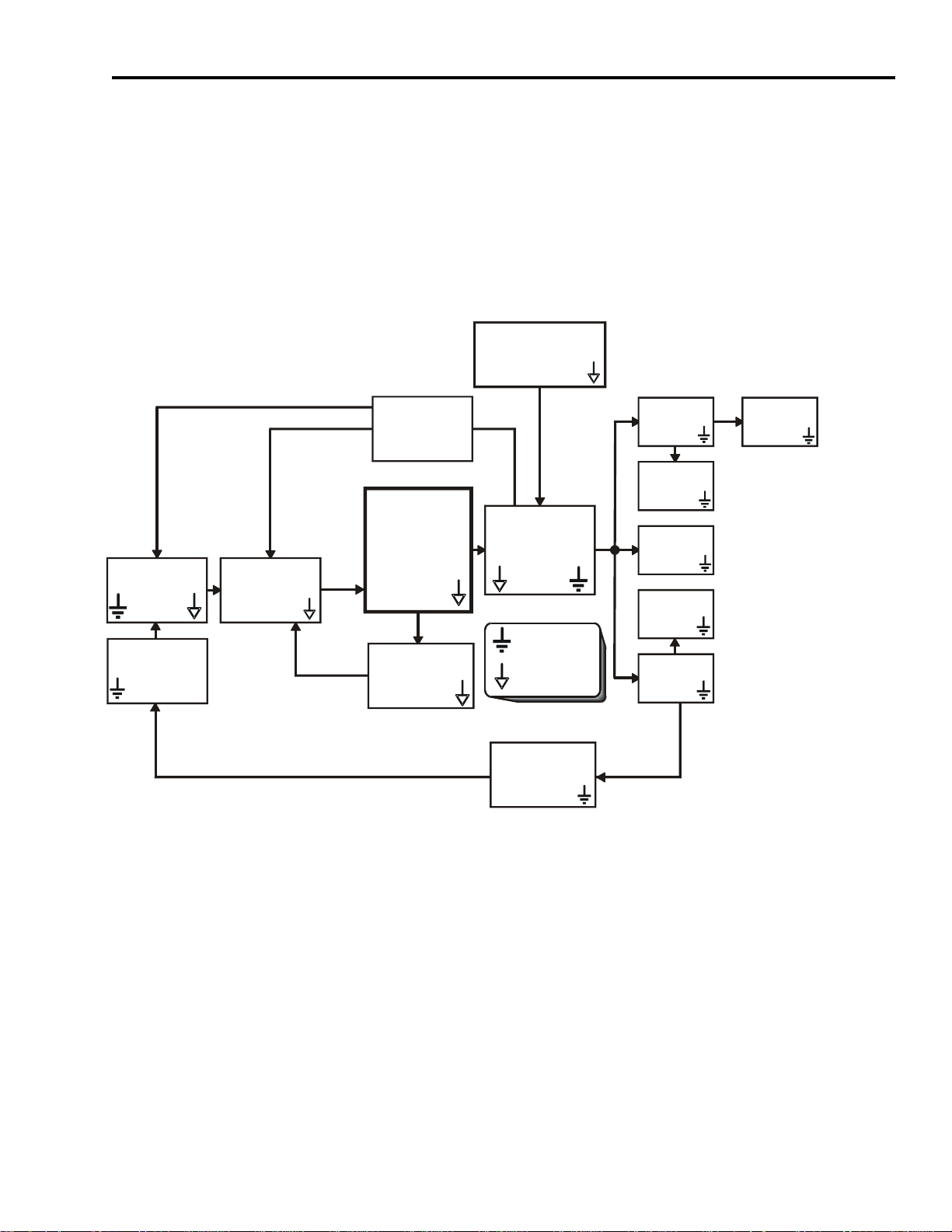
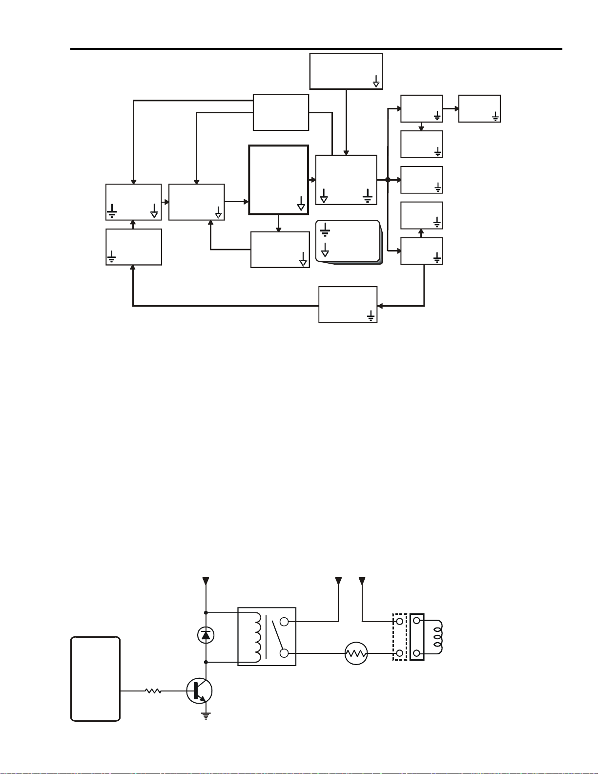
The main power circuits supply many different voltages to the CTC203 chassis.
Figure 2-1 is a block diagram showing the voltages generated and their derivations
from the main power. Notice all standby voltages are derived from Raw B+.
However, differing from most previous chassis', the main supply generates all low
voltages required during Run, Standby and Data Acquisition modes of operation.
All voltages, except the switched and scan derived, are available any time the AC is
connected to the line. Mainly, they supply the microprocessor, infrared remote
control detection and tuning circuitry during standby. All other voltages are derived
from the main supply and switched on during run or data acquisition modes.
The main supply generates voltages for normal operation of all other circuits and
components. In addition, many of the supplies are used to generate the remainder of
the low and high voltages required by the chassis.
The Technical Training Manual will discuss the power supplies in this order; Main,
Switched (SW) and Scan Derived.
Raw B+
Power Supply 11
OPTO-ISOLATOR
U14101
PRECISION
REGULATOR
U14102
BIAS
SUPPLIES
OUTPUT
POWER
TRANSFORMER
T14101
Cold Ground
Hot Ground
Reg B+
Feedback
CONTROL
LATCH
Q14102/103
POWER
OUTPUT
Q14101
OVER-CURRENT
OVER-VOLTAGE
R14108
Figure 2-1, CTC203 Main Power Supply Block Diagram
+16Vr
+5.2Vs
-12Vr
+33Vs
Reg B+
+7.6Vr
12 Power Supply
Standby Supply Overview
The standby supply is a new class of high power, ZVS (Zero Voltage Switching)
supply developed to minimize switching losses and radiated noise. A return to
discrete devices lowered parts count and decreased circuit board space utilization.
ZVS refers to the ability of the supply causing the voltage across the principal power
output device, to reduce to near zero before the device is switched on. Yet it has a
slow enough time lag to allow the device to switch off completely before any
appreciable voltage is present across the device. This can better be illustrated in
Figure 2-2.
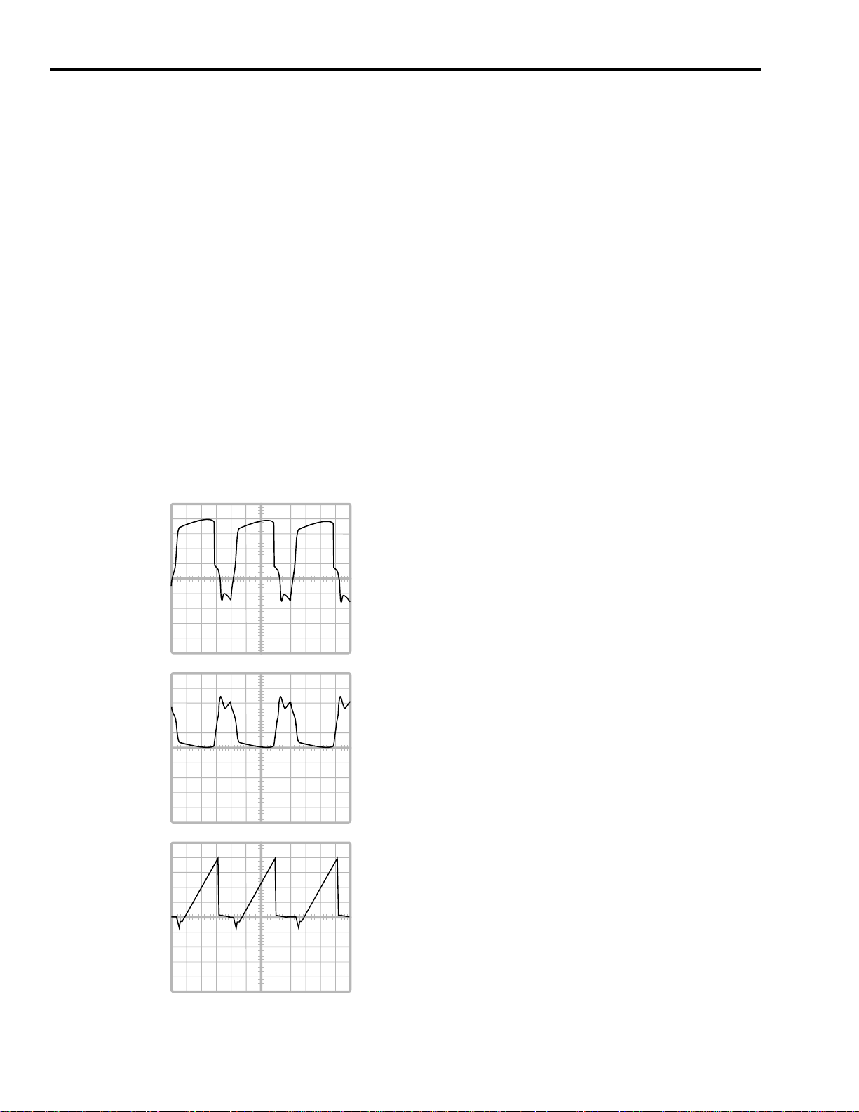
Note that the first two waveforms are voltages, while the third is current. The
MOSFET begins conducting current when the gate voltage reaches the proper turn
on point. From that time, output current rises linearly due to the inductance of the
output transformer. However, notice that once the gate voltage goes high, the drain
voltage decreases almost to zero volts. This eliminates much of the heat dissipation
normally required of an output device.
Q14101
Gate Voltage
Q14101
Drain Voltage
By reducing the switching losses to almost
zero, the efficiency of the power supply is
greatly increased and the limiting of the
switching voltages causes a substantial
reduction of switching noise.
Also note that by utilizing the resonant
recapture of energy stored in the leakage
inductance of the output transformer, neither
a snubber nor a clamp is required, leading to
improved efficiency and lower parts count.
Q14101
Drain Current
Figure 2-2, Power Supply Output Device Waveforms
Power Supply 13
Digital Latches
Before wading deeper into the CTC203 power supply, the technician should become
familiar with the control circuitry used to turn the power output devices on and off. It will
be common to various ZVS supplies used throughout this and other TCE chassis'.
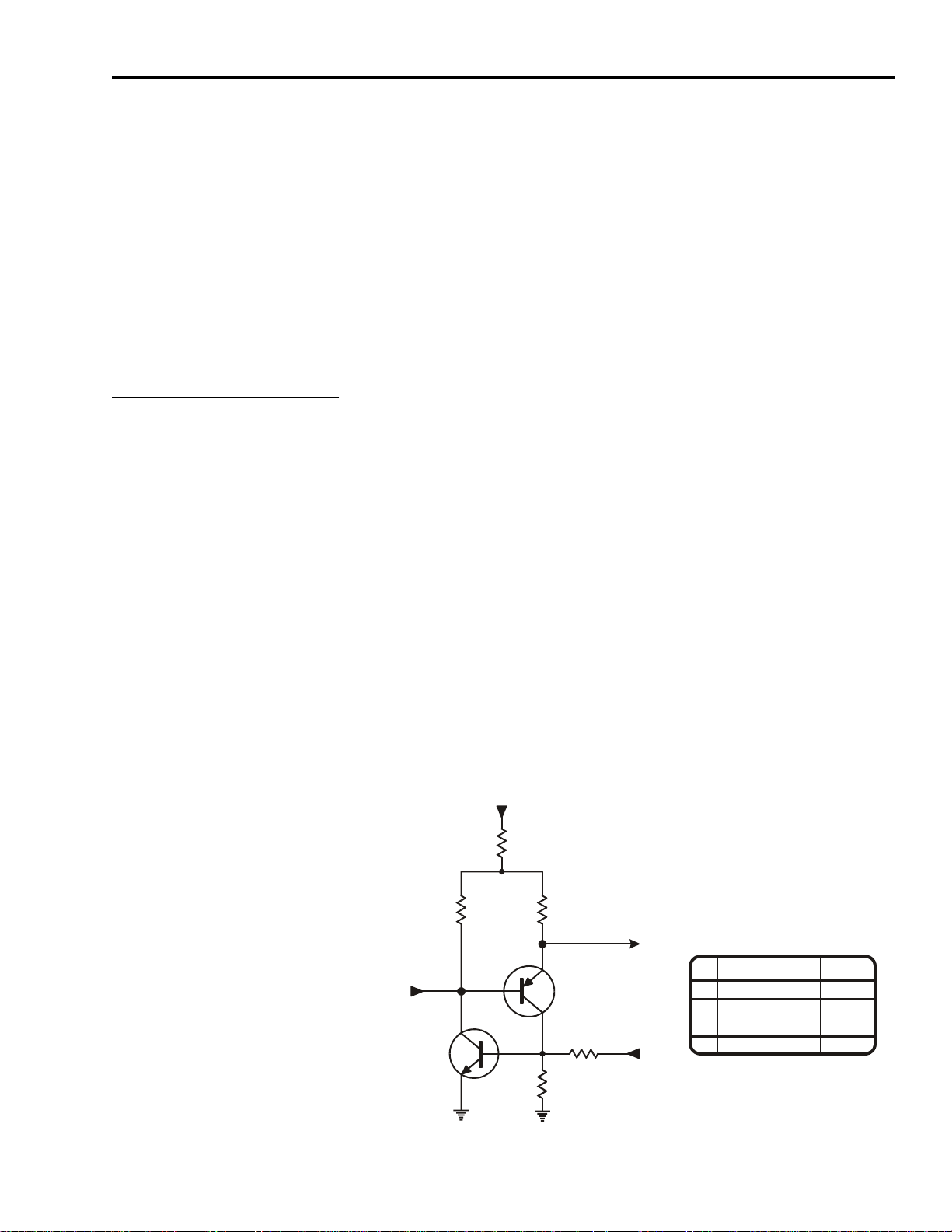
The control switches act similar to an SCR, but with a few variations. Figure 2-3 shows a
truth table and simplified schematic representaion of the power supply control latch shown
in Figure 2-4. Again, while the other ZVS supplies may have slight variations, the basic
concept and operation is the same.
Q1 and Q2 form the basic latch circuit. Both are switching transistors that saturate when
tripped on. In this case an NPN and PNP are used to force the desired results on the output.
The latch is controlled by placing or removing voltages on either base while sufficient
voltage is present on Q2-E to set the latch. Keep in mind
B+ will supply drive to the output
when the latches are off!!! The latch REMOVES the output. Any time the truth table
shows a low (0) condition, output is removed.
In condition A, both IN1 and IN2 are low (0). A low in Q2-B turns it on providing a current
path from B+ through R5, R2, Q2-E/C and R3 to ground. Sufficient bias is developed
across R3 to turn Q1 on, setting the latch. Now, regardless of what happens on IN1, the
latch is set. The combined voltage drop on R3 and Q2-E/C places Q2-E at a very low
voltage, shutting the output off.
If IN2 goes high (1) as in condition B, there will be no effect on the output. The high on
IN2 would turn Q1 on, but since it is already on the result is no change in the output state.
In condition D, both inputs are high. A high on Q1-B turns it on. When it turns on it
saturates, bringing Q2-B low, turning it on. When it turns on the latch is again set and the
output goes low.
Condition C is the most difficult to understand because it relies on the input voltages being
different before the latch is tripped. If IN1 is high, the latch state is dependant upon IN2 for
its output state. If IN2 is low, the output is high. If IN2 is high, the output is low.
However, if the latch is set
(tripped) Q2 saturates and holds
B+
Q1 on even with IN1 high. What
has to happen before the latch
will trip off is the loss of bias on
R5
680K
Q1-B.
As IN2 decreases it begins to
divert current flow away from
R3 and its voltage drop also
begins to decrease. The voltage
on Q1-B will eventually drop low
enough for it to shut off. If IN1
is still high Q2-B is now high
and it also shuts off. This
removes both Q1 and Q2 from
R1
1000
Q2
IN 1
Q1
R3
3300
R2
1000
R4
1000
Out
IN 2
IN1 IN2 O UT
A
00 0
B
01 0
C
11 0
D
011
the circuit and B+ now supplies
the output voltage.
Figure 2-3, Digital Latch & Truth Table
14 Power Supply
Control Latch Review
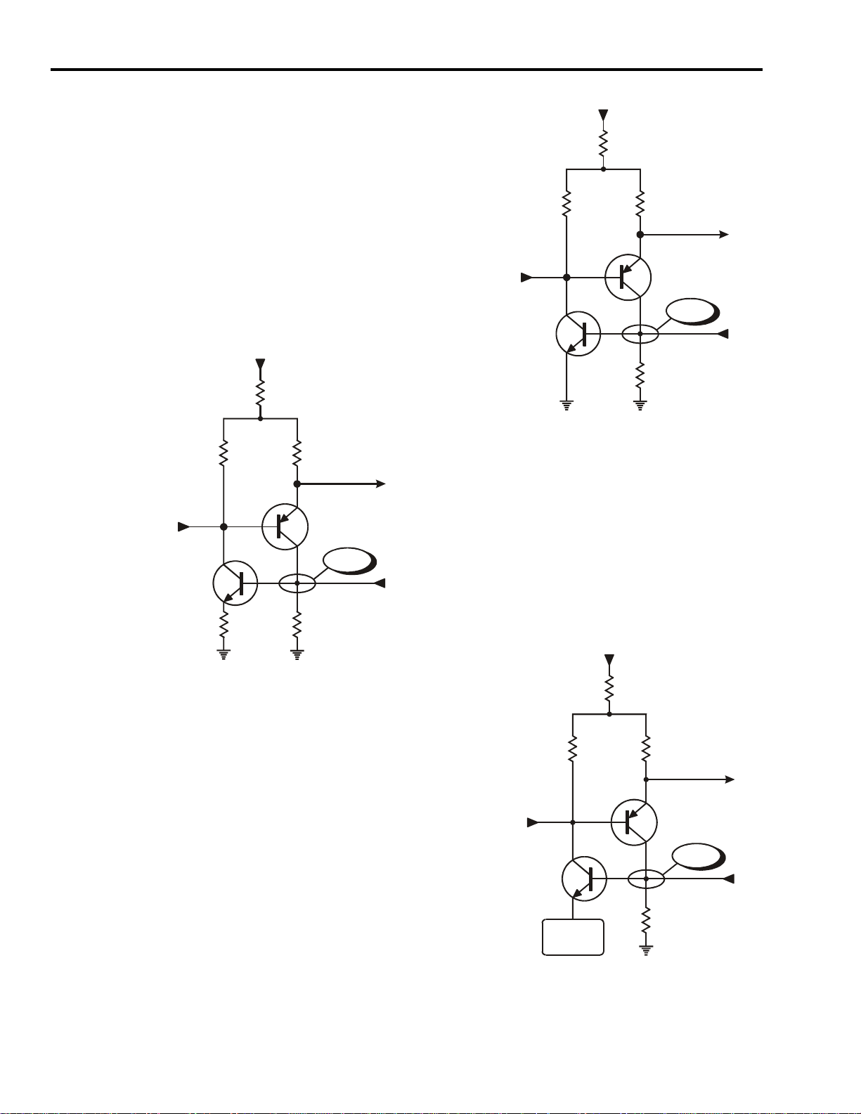
Now that the digital latch operation is
understood, it needs to be shown how it is used
to regulate the CTC203 power supply. Using
the simplified digital latch schematic from the
previous page, when IN1 is high, IN2 may be
used to control the output. When IN2 is high,
the output is low. When IN2 is low, the output
is high. In Figure 2-4A, Q1-E is grounded.
Normal PN junction drop of a transistor dictates
that a bias of at least +0.6V must be placed on
Q1-B to turn it on.
B+
R5
680K
R1
1000
Q2
IN 1
Q1
R2
1000
+1.0V
Out
IN 2
In Figure 2-4B a resistor (R5) has been placed
in the emitter circuit of Q1. The resistance of
R5 reduces the amount of current through the
PN junction of Q1E/B with the same voltage
on Q1-B. Thus, to increase current high
enough to turn on Q1, Q1-B voltage must
R5
1000
R3
3300
increase. In this case to about +1.0V.
B+
R5
680K
R1
1000
Q2
IN 1
Q1
R3
3300
R2
1000
+0.6V
Figure 2-4A, Digital Latch Normal
B+
Out
IN 2
Figure 2-4B
In Figure 2-4C Q1-E is connected to a
negative 5V supply. The current to turn
the PN junction of Q1 on remains the same.
Now the voltage on Q1-B need only be
0.6V higher than Q1-E, or about -4.4V.
In this manner, the voltage that triggers Q1
may be varied and used to control the output
of the latch. By understandby this circuit,
the regulation and protection of the power
supply may be more fully understood.
IN 1
R1
1000
Supply
Q2
Q1
-5V
Figure 2-4C
R5
680K
R2
1000
Out
-4.4V
IN 2
R3
3300
Latch Circuit
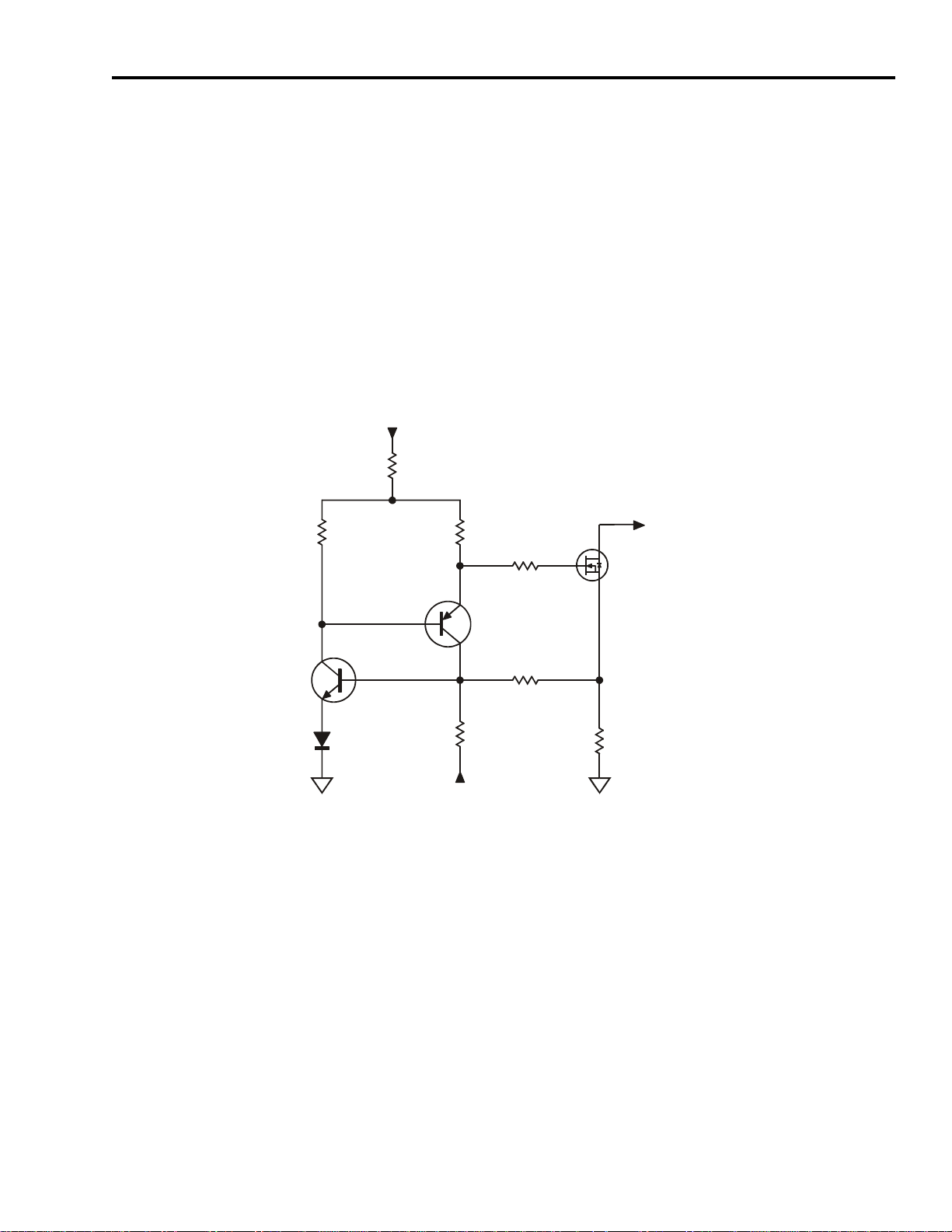
Figure 2-5 is the control latch for the CTC203 power supply. It is not much different
from the simplified schematic in Figure 2-3, however there are some additional
circuits that will need to be discussed later.
When power is first applied to the chassis, Raw B+ is available on the "IN1" line at
the junction of Q14103-C and Q14102-B. Since there is no bias difference from
Q14102B-E, it is off and the latch is off. Raw B+ now supplies gate drive to the
output device Q14101-G, turning it on providing output transformer current. At this
time, "IN1" is high, IN2 is low and the latch is off, allowing gate drive.
As current builds in the output device, a voltage is developed accross R14108.
When this voltage increases enough, it will bias Q14103 on, which also turns on
Q14102, setting the latch. A current path now exists between Raw B+, R14103,
R14106, Q14102-C/E, R14110 and a negative bias voltage developed from the
output transformer.
R14104
3300
Raw B+
R14103
1Meg
R14106
1000
OUT
R14107
43
To Output
Transformer
T14101
Q14101
Power Supply 15
Q14102
IN1
Q14103
R14109
750
IN2
R14110
CR14105
22K
Positive Bias
Supply
Figure 2-5, Power Supply Control Latch
Once the latch is set, Q14102-E voltage and output drive is removed and the output
device, Q14101 shuts off. With output current dropping, the corresponding voltage
drop across R14108 begins to decrease along with the negative bias supply. At some
point the voltage at Q14103-B drops low enough to allow it to turn off. When it
does, bias is removed from Q14102-B and it shuts off. When it shuts off, gate drive
is again allowed to turn the output device, Q14101 on and output current begins to
build once more.
As the power supply circuits develop, it will be seen that by either varying the bias
voltage on Q14103-B while maintaining the voltage on Q14103-E, or varying the
bias on Q14103-E, while maintaining the voltage on Q14103-B, the on/off time of
the latch can be controlled precisely. Controlling the latch means output current is
also controlled. The off time of the latch is reasonbly constant. It is the "on" time of
the output that controls the supply voltages.
R14108
0.1
3W

16 Power Supply
Main Supply Block Diagram
The Main Supply distributes power to all devices that need to remain "alive" when
the chassis is "off". In addition, it must retain enough power to keep the
microprocessor active during a power failure event long enough to exercise the
"batten down the hatches" routine leading to a graceful shutdown of the chassis
before power disappears completely. ("Batten" is a software routine which stores
off all customer settings and chassis alignments to the EEPROM. This enables the
set to start normally after a catastrophic power failure.)
The voltages available during standby operation are:
•-12 volts
•+5.2 volts
•+7.6 volts
•+16 volts
•+33 volts
•Reg B+
The supply converts raw B+ from the incoming AC line into the various DC supplies
required by the CTC203. There is a "Data Acquisition" mode requiring greater
current supply demands from the supply than normally needed during standby, but
less than is needed during full run operation. For instance, during a TVGuide+
download, there is no reason for the set to display a picture, however, the tuner must
be active to receive the signal. This requires more current from Reg B+ from which
the +33V supply is derived.
Since the forward conduction mode is used, the driver current is proportional to the
supply current and higher frequencies (70-90 kHz) may be used for greater efficiency.
The standby supply may be broken into several sections according to Figure 2-5.
The Latch circuit (discussed previously) consists of Q14102 and Q14103. They
control the off/on time of the output device, Q14101.
Current in the output power transformer, T14101, transferred to the secondary, is
used to generate the various supplies from Raw B+ provided by the main rectifier
from incoming AC.
The regulator, U14102 and opto-isolator, U14101 provide regulation of the +16Vs
supply and isolation between the cold ground run supplies and the hot ground
generator circuit components.
Overcurrent and overvoltage protection of the output device is provided by resistor
R14108 in series with Q14101.
Raw B+
Power Supply 17
OPTO-ISOLATOR
U14101
PRECISION
REGULATOR
U14102
CONTROL
LATCH
Q14102/103
BIAS
SUPPLIES
POWER
OUTPUT
Q14101
OVER-CURRENT
OVER-VOLTAGE
R14108
OUTPUT
POWER
TRANSFORMER
T14101
Cold Ground
Hot Ground
Reg B+
Feedback
+16Vr
+5.2Vs
-12Vr
+33Vs
Reg B+
+7.6Vr
Figure 2-6, CTC203 Main Supply Block Diagram (Standby Voltages)
AC Input and Degaussing
Raw AC is connected using protection (F14200) and filtering/smoothing components
to assure spikes and unexpected surges do not cause catastrophic failure.
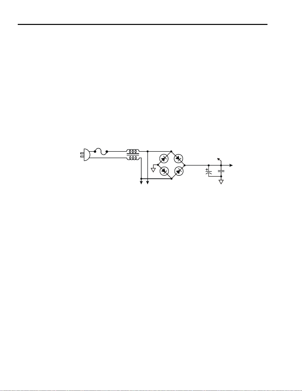
Degaussing may only be done when the +12V run supply is active. System Control
sends a high out during startup turning on Q14201. As long as the +12Vr supply is
up, relay K14201 is turned on activating the contacts on pins 3 & 4. Current from the
AC line is now routed to the degaussing coil. Degaussing occurs as long as thermal
resistor RT14250 allows. It provides an exponential decay of current to the degaussing
coil. Degauss current must be allowed to decay before the relay stops all degauss
coil current to allow proper degaussing, otherwise color non-uniformity will result.
When System Control removes the active deguass signal, Q14201 shuts off, removing
drive current from the relay coil, breaking the contacts and removing AC power
from the degaussing coil. The degaussing cycle is then complete.
Figure 2-7, Degaussing
From Incoming
AC Line
RT14201
DEGAUSSING
COIL
J14203
U13101
SYSTEM
CONTROL
45
Degauss: High
R14206
1000
CR14250
+12VrSW
Q14201
1
2
K14201
4
3
18 Power Supply
Raw B+
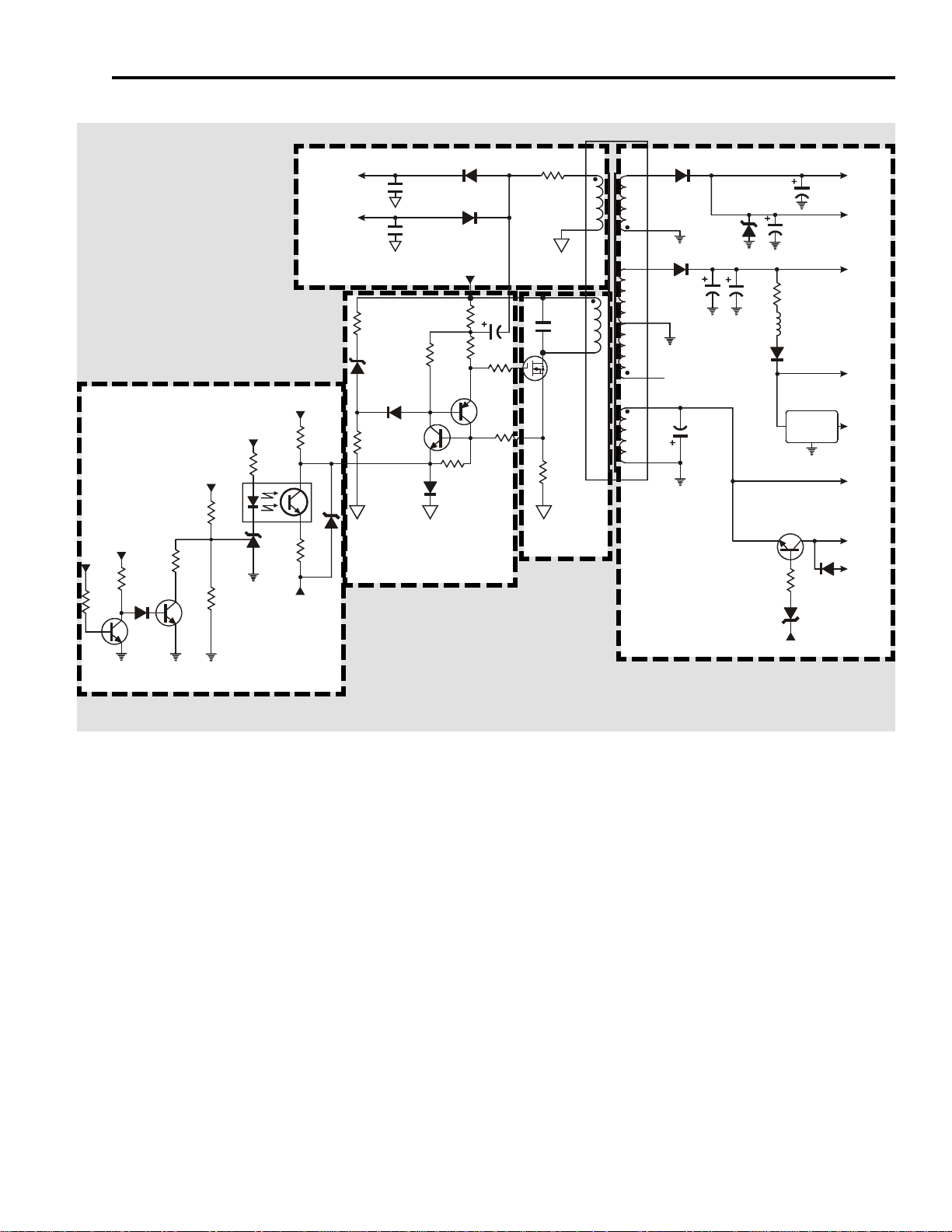
Incoming AC (95 - 135 VAC) is input through an LCI (Line Conducted Interference)
filter consisting mainly of T14201 and several filter capacitors. Raw B+ is generated
from the incoming AC by a discrete bridge rectifier circuit consisting of CR14201,
CR14202, CR14203 and CR14204. Main power supply input voltage is 95-135
VAC to provide a Raw B+ voltage of about +156V depending upon the chassis
version. Generally, larger screen sizes will require higher raw B+.
F14201
120VAC
5A
T14201
To DeGauss
Circuit
CR14201CR14202
TP14210
Raw B+
C14205
680uF
CR14203CR14204
156VDC
C14206
0.012
Figure 2-8, AC Input
Power Supply 19
+13Vr
R14128
680K
+16Vs
R14127
10K
CR14111
Q14107
R14115
143K
R14126
37.4K
Q14106
RegB+Vs
R14116
2000
+16Vs
R14113
1300
U14101
U14102
R14112
680
Pos Hot
Bias Supply
Neg Hot
Bias Supply
CR14101
Pos Hot
Bias Supply
R141111
Neg Hot
Bias Supply
Bias Supplies
C14104
0.047
C14108
0.047
R14101
47K
R14104
CR14102
R14102
6800
3300
Q14103
CR14105
10K
47V
CR14117
16V
Control
CR14103
CR14104
R14103
1Meg
R14106
2000
R14110
22K
RAW B+
C14101
2.2uF
R14107
43
Q14102
R14109
750
R14105
10
C14108
1100
1.6KV
Q14101
R14108
0.1
3W
Drive
3
8
9
5
T14101
C14122
33uF
C14114
3.3uF
L14102
R11513
4700
CR11504
18V
Output
C14122
33uF
R14124
3.3
2W
CR14110
U14103
+5.2V
Reg
Q11501
CR11505
+12VrSW
Reg B+
+33Vs
+16Vs
+7.6Vs
+5.2Vs
-12Vs
-12Vr
-12V
Fil
CR14106
16
CR14108
C14121
3.3uF
CR14107
C14116
47uF
33V
14
15
13
NC
10
11
12
Feedback/Regulation
Figure 2-9, Main Power Supply
Main Supply Operation
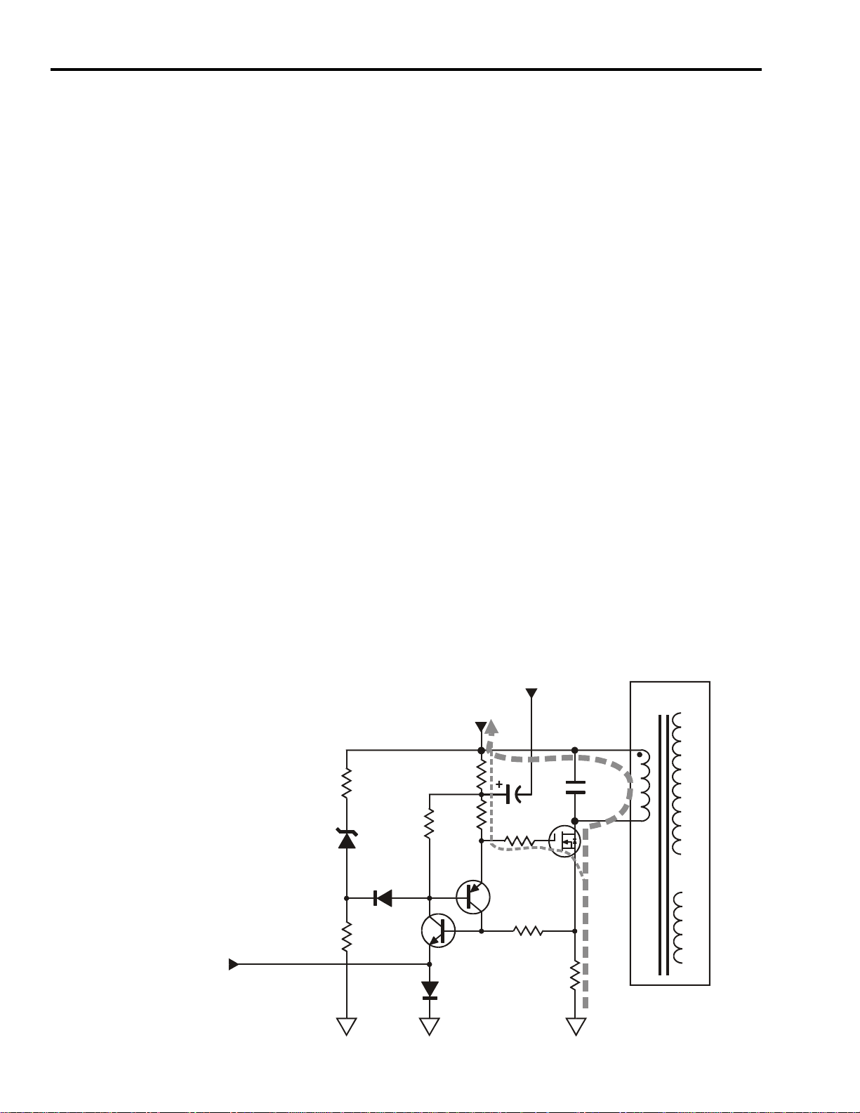
To simplify the understanding of the standby supply (shown in Figure 2-9), it will be
broken down into smaller blocks. These blocks operate somewhat independently,
but ultimately must all function together for proper operation of the supply.
The sections are:
Output
Drive
Control
Feedback/Regulation
Bias Supplies
20 Power Supply
Standby Supply Startup
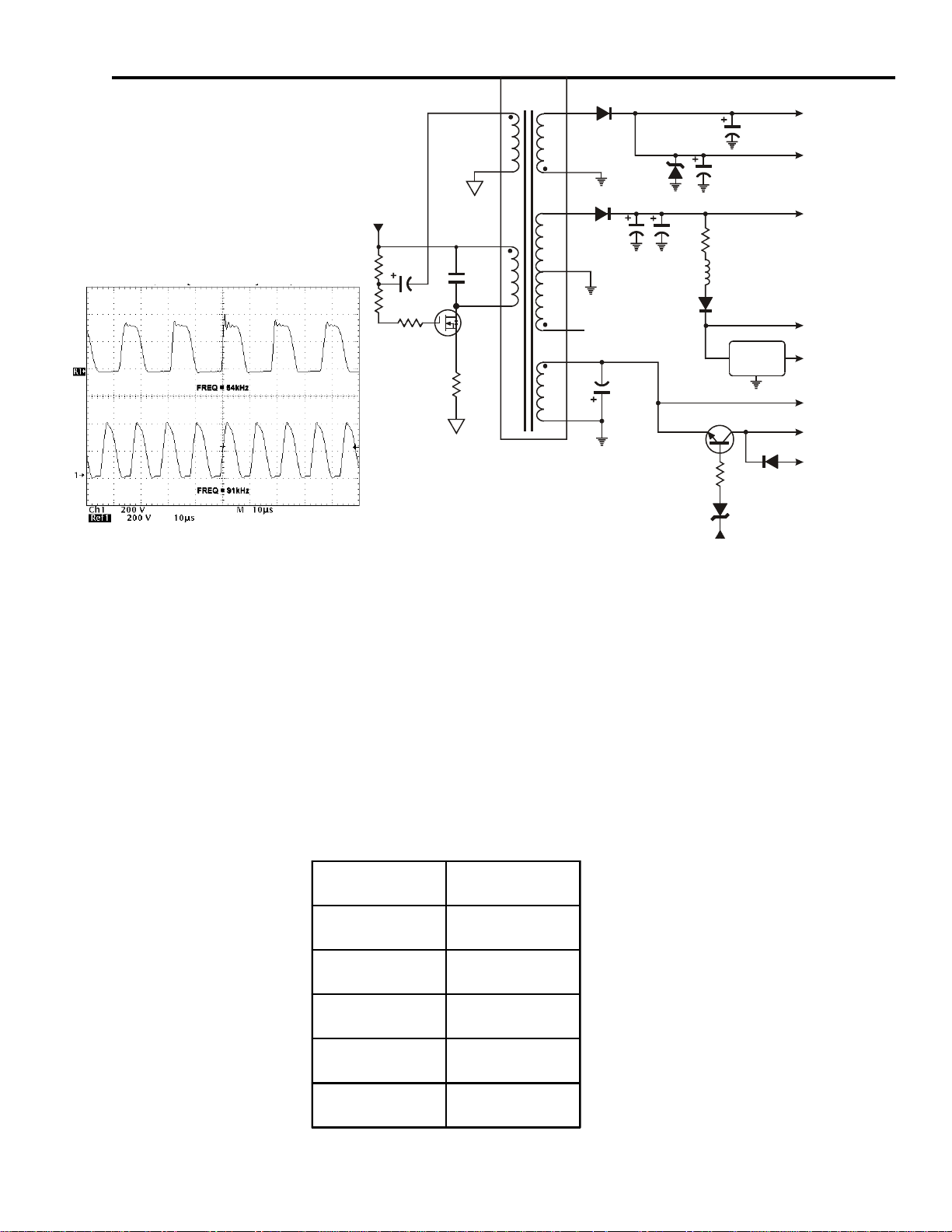
A voltage divider network from Raw B+ consisting of R14103 and R14107 provides
the initial positive gate voltage for output MOSFET Q14101 to begin conduction. As
current begins to flow in the output transformer T14101, winding 3/8, feedback current
is induced to windings 1/2. This winding provides several bias voltages to the supply
drivers and feedback circuit, but initially is used to increase the gate voltage, using
C14101 to couple the transformer to the gate. The voltage at pin 9 is increasing in a
positive direction as current increases in the primary. This rising voltage eventually
causes the output, Q14101, to saturate, beginning the first cycle of operation.
As current through Q14101 increases, the voltage drop across current sense resistor
R14108 increases until a threshold is reached. (This threshold is discussed in the
control latch section.) At the time the threshold is reached, the regenerative switch
(latch circuit) consisting of Q14102/Q14103 turns on, removing gate drive from output
device Q14101.
Current flow through Q14101 drops quickly to zero and energy stored in the transformer
primary winding is transferred to C14108 which charges with the negative potential at
Q14101-D. This rising voltage appears across the secondary winding.
When the secondary side of the transformer conducts, the energy stored in the primary
of T14101 is delivered to the secondary supply capacitors and the load. After the
secondary diodes stop conducting, energy still contained in C14108 drives the drain
voltage of Q14101 toward zero. When the drain voltage attempts to go below zero, an
internal diode clamps it near ground.
Now the voltage of T14101 drive winding, 5/9, goes positive and if the latch circuit
allows it, will turn on Q14101 and the next cycle begins. Once the initial startup pulse
from Raw B+ starts the cycle, this bias supply takes over and continues to supply gate
drive to the output device.
Bias Supply
from T14101
From
Regulator
Circuits
CR14101
47V
R14102
6800
R14101
47K
R14104
CR14102
Q14103
CR14105
3300
RAW B+
R14103
1Meg
R14106
2000
Windings 9/5
C14101
2.2uF
R14107
43
Q14102
R14109
750
C14108
1100
1.6KV
Q14101
R14108
0.1
3W
Part of
T14101
3
8
Figure 2-10, Power Device Start up Current Flow
RAW B+
C14101
2.2uF
R14107
43
R14108
0.1
3W
Bias Supply
Windings
C14108
1100
1.6KV
Q14101
9
5
3
8
T14101
Power Supply 21
CR14106
16
C14122
33uF
C14114
3.3uF
L14102
R11513
4700
CR11504
18V
C14122
33uF
R14124
CR14110
Q11501
3.3
2W
U14103
+5.2V
Reg
CR14108
C14121
3.3uF
CR14107
C14116
47uF
33V
14
15
13
NC
10
11
12
Reg B+
+33Vs
+16Vs
+7.6Vs
+5.2Vs
-12Vs
-12Vr
-12V
Fil
Figure 2-11, Main Supply Output
+12VrSW
Output
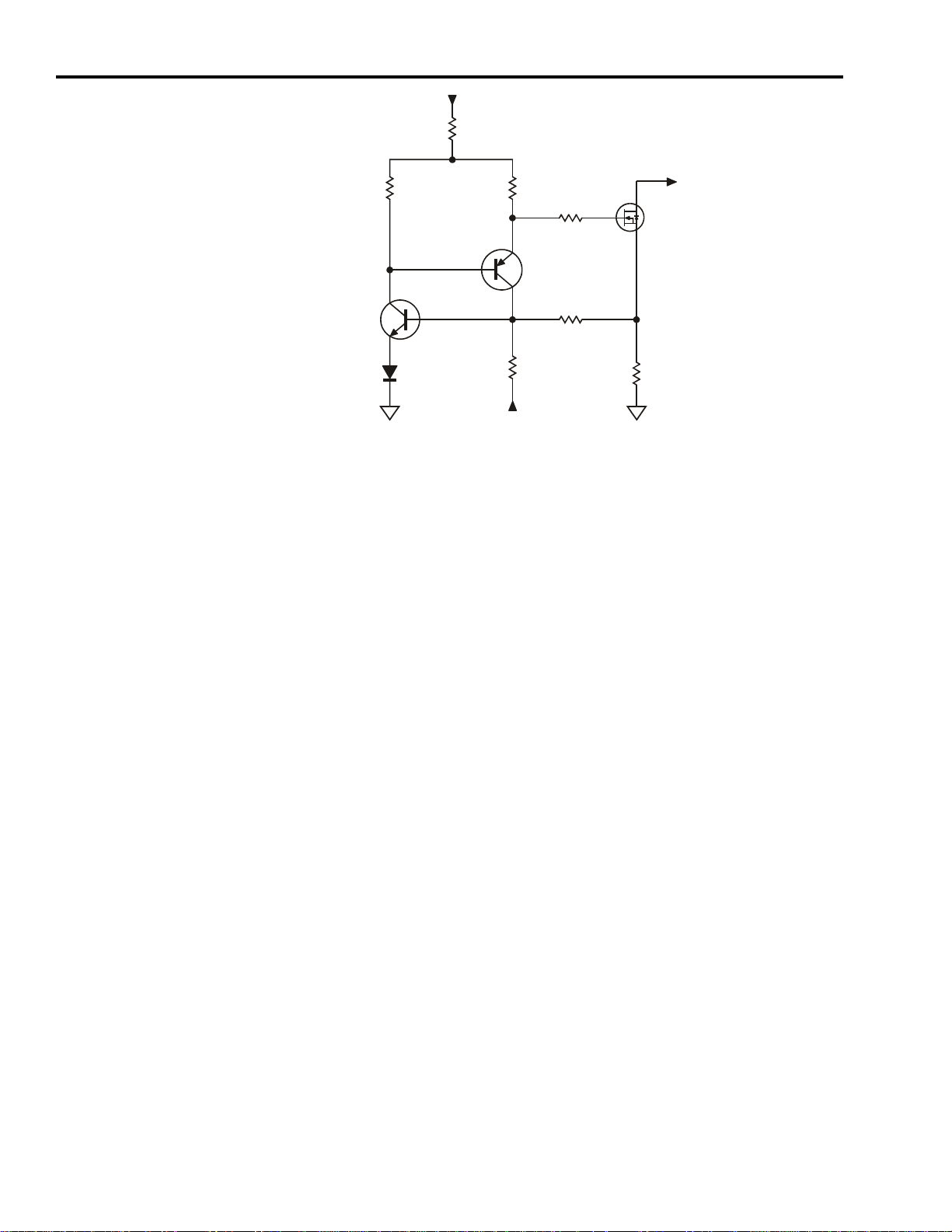
Q14101 provides all transformer primary winding drive current. It is a power mosfet
which conducts current from source to drain when the gate voltage is high. Once on,
gate voltage must be reduced to around zero or the drain-source current path must be
interrupted to stop output current. During conduction, current flows from common
(hot) through R14108, Q14101 and T14101 primary winding to Raw B+. C14108 is
used to "tune" the resonant frequency of the primary for better power transfer.
Normally this frequency is around 90kHz during standby and 40-60kHz during run
operation. Figure 2-11 shows the driver and output voltages and a waveform
comparing Q14101-D outputs in standby and run mode. As current flows through
the primary, flux lines induce current flow into secondary windings 5/9, 11/12,
13/15 and 14/16. Typical AC voltages generated from the windings are shown in
Figure 2-12.
T14101 Pin# AC Voltage
3/8 400 p-p
5/9 15 p-p
11/12 26 p-p
13/15 35 p-p
14/16 250 p-p
Figure 2-12, Typical Secondary Winding Voltages
22 Power Supply
R14104
3300
IN1
Raw B+
Q14103
R14103
1Meg
R14106
1000
OUT
IN2
Q14102
R14107
43
R14109
750
To Output
Transformer
T14101
Q14101
CR14105
R14110
22K
Positive Bias
Supply
R14108
0.1
3W
Figure 2-13, Main Supply Output Drive Control
Standby Supply Drive
To assist the understanding of the control circuit, this discussion will not take the
positive bias supply in consideration at this time. Operation of the control circuit
will be identical.
At initial startup, R14103 provides the gate voltage to turn Q14101 on, providing
primary current. As Q14101 begins to conduct, primary winding current increases,
increasing voltage across the winding and inducing current flow to all secondary
windings. Q14101 quickly saturates.
R14108 monitors the primary winding current, which is also the current through the
output device, Q14101. As this current increases, the corresponding voltage drop
across R14108 increases. When it reaches a voltage high enough to turn Q14103 on,
the latch "sets" stopping drive to the output, Q14101. It does this do to a current path
from common through CR14105, Q14103-E/B, Q14102, R14106 the gate drive
being developed by C14101 and T14101 windings 5/9. Q14102 emitter drops to a
low voltage, shutting the output device Q14101 off. This cuts current flow to the
primary of T14101. Without drain current, drain voltage now increases due to back
EMF across the transformer windings. The secondary diodes conduct and power is
delivered to the loads. C14108 helps shape the waveform, limiting conduction time
as Q14101 shuts off and drain voltage is driven to zero.
Two things are now happening. First, with Q14101 now off, primary current flow
begins to decrease. Second, with current flow in the primary and output stopped, the
voltage across R14108 now decreases below the bias point of Q14103 and it shuts
off, shutting off Q14102. The bias supply developed from T14101-5/9 and C14101
now supplies gate drive and the output, Q14101 turns back on. The process now
begins again.
Bias Supplies
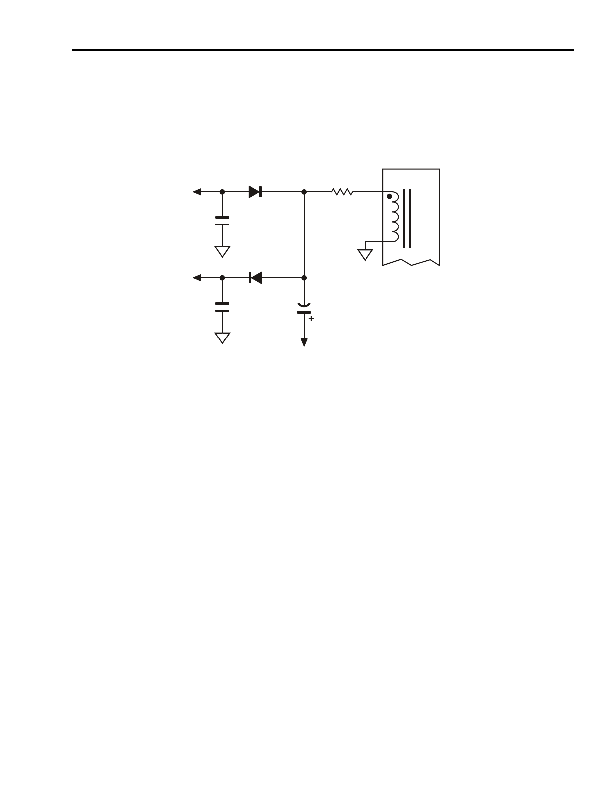
There are two supplies generated during standby supply operation used to internally
bias the control and regulation components of the supply. Both cycles of the
transformer waveform are utilized to provide a positive and negative supply voltage.
These voltages vary with respect to the current flow in the primary winding of
T14101 but should normally be within the 5 to 10 volt range, positive and negative
respectively. An unrectified pulse is used as the initial gate pulse to saturate the
output device.
Negative Supply
Source
(app -5 to -15V)
CR14104
C14066
0.047uF
R14601
100
T14101
9
5
Power Supply 23
Positive Supply
Source
(app +5 to +15V)
CR14105
C14103
0.047uF
C14101
2.2uF
To Q14101-G
Figure 2-14, Bias Supplies
Standby Supply Control
Without some form of regulation, the power supply will quickly reach a nominal
output voltage using the control circuit in Figure 2-13. Figure 2-15 again shows the
control circuitry, but adding regulation to keep the output voltages from the secondary
of the supply within design limits. Load variations are constant and there is the
problem of loads outside the normal expected variations to deal with. The main
supply is required to provide standby and run power to some circuits, further
complicating load demands.
All this means that the supply must be regulated and protected against overload
conditions. An opto-isolator protects the "hot" primary side of the supply from the
"cold" secondary side and is also used for regulation.
Referring back to Figure 2-13, it may be seen that by varying the on/off time of the
latch, Q14102 and Q14103, output current can also be varied. For instance, the trip
voltage required to turn Q14103 on with diode CR14105 in its emitter circuit is
about +1.2V. This assumes a PN junction IR drop of 0.6V for the diode and 0.6V for
the emitter-base junction of the transistor. If a second diode were placed in series
with CR14105, the trip voltage would now be +1.8V. (Of course, with the added IR
drop of R14109, the voltage would need to be greater.) If CR14105 were removed,
the trip voltage now would be lower by 0.6V or about +0.6V.
Now it can be seen that regulating the output current by varying IN2 is a matter of
either increasing the voltage on Q14103-B, or lowering the voltage on Q14103-E.
Either method achieves the same results. This technique may be used to provide
regulation of output current.
24 Power Supply
Main Power Supply Regulation
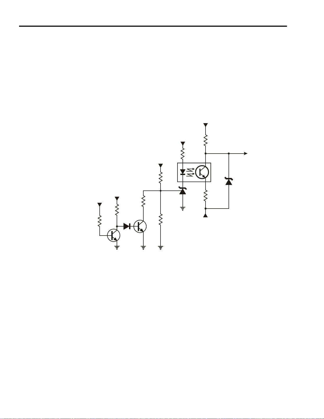
To provide regulation of the control latch which in turn varies the secondary
voltages, a regulation circuit is used. Since the regulator is monitoring secondary
voltages which use "cold" ground, and manipulating circuits on the primary or "hot"
side of the power supply transformer, the regulator must also provide isolation.
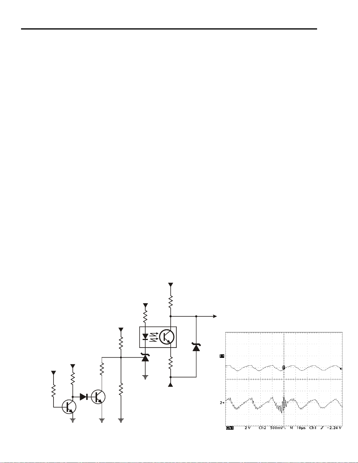
Initially, a bias voltage is set up on Q14103-B by a voltage divider network between
the positive and negative bias supplies. R14112, the output of U14101 and R14111
make up this network. Since the supplies are constantly changing do to primary
current, they are difficult to measure, however when operating normally the nominal
voltage on Q14103-B is very close to zero.
A feedback voltage, Reg B+, is used to monitor the secondary voltages generated by
the main supply. If Reg B+ increases such that the junction of R14115 & R14116
rises above +2.5 volts, the internal impedance of U14102 (See the Tech Tip on this
new device) decreases. Increased current through the device turns on
opto-isolator, U14101 harder and the output impedance of this device decreases.
This output is in the voltage divider network between the negative and positive bias
supplies. As the impedance decreases, the voltage on Q14103-E goes more negative.
It now takes less voltage on Q14603-B to trip the control latch to the "ON"
condition. Remember that when the latch is on, gate drive is removed from the
output device, Q14101, and output current stops. Secondary supply voltages begin
to drop.
R14128
680K
+13Vr
The waveform shows voltage levels on the emitter of U14101 (Top) and the collector
(Bottom). The emitter is essentially the negative supply ripple. The DC level is
about -11V. The internal impedance of the output section is increasing and decreasing
at such a rate that under normal load levels it fluctates closely around 0V.
Pos Hot
Bias Supply
+16Vs
R14127
10K
CR14111
Q14107
R14115
143K
R14126
37.4K
Q14106
+16Vs
R14113
1300
Reg B+
U14101
U14102
R14116
2000
R14111
10K
R14112
680
Neg Hot
Bias Supply
To Control
Q14103-E
CR14117
16V
Figure 2-15, Standby Supply Regulation
Power Supply 25
When Reg B+ drops sufficiently, the junction of R14115 & R14116 drops below
+2.5V. Now the internal impedance of U14102 increases. As it increases, the output
section of the opto-isolator, U14101 is driven less and its impedance also increases.
The voltage on the collector of U14101 now goes towards the positive supply. This
voltage is also on Q14103-E. It now takes more voltage on Q14103-B to turn the
control latch off. Gate drive is allowed on the output, Q14101 and primary winding
current is again available in T14101. As current in the primary increases, voltage in the
secondaries also increases and the cycle repeats.
If a failure occurs in the regulation circuits such that the output of U14101 opens, the
positive hot supply is placed on Q14103-E. Output current is now stopped only by the
overvoltage/overcurrent protection provided by R14108, which is acting as a current
monitor for the output device.
If the failure mode shorts U14101 output or places it in a low impedance mode, the
negative hot supply, only limited by R14112 appears on U14101-C and thus Q14103-E.
It now takes very little output current to trip the latch and remove output drive. All
supplies will be reduced and not maintain any regulation.
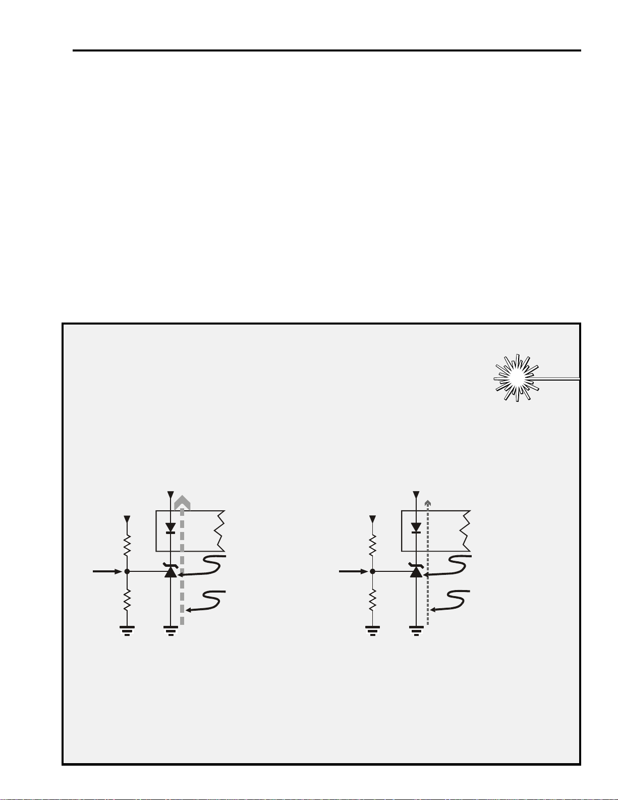
Precision Shunt Regulator
The three terminal precision shunt regulators used throughout the various supplies
of the CTC203 are unique devices. They may be thought of as "gated" zener
diodes, or infinite gain operational amplifiers with a reference voltage tied to the
negative input. In both cases, for the CTC203 chassis, 2.5V is the reference
voltage.
Figure A shows the regulator when the reference voltage on pin 1 is above 2.5V. The
regulator conducts, its internal impedance decreases, and current through the device
increases.
>2.5
R14115
143K
0.1%
R14116
2000
0.1%
Reg B+
U14102
+16Vs
1
3
2
U14101
Decreased
Internal
Impedance
Increased
Current Flow
Reg B+
R14115
143K
0.1%
<2.5
R14116
2000
0.1%
U14102
+16Vs
1
3
2
U14101
Increased
Internal
Impedance
Decreasing
Current Flow
TECH
TIP
Figure A Figure B
Figure B shows the regulator when the reference voltage on pin 1 is less than 2.5V. The
internal impedance of the regulator increases and current flow through the device
decreases.
In both cases, the current through the regulator directly drives the LED side of the
opto-isolator. As this current increases, the output impedance of the opto decreases.
As current decreases, the output impedance increases.
26 Power Supply
Run Mode
In order to supply the different current demands between standby and run modes, the
main supply monitors the +13Vr supply generated from scan. If the supply is
running, Q14107 is on, turning off Q14106. This removes R14126 from the
regulator circuit and supply operates normally.
When scan is lost, the +13Vr supply is removed turning off Q14107. This turns on
Q14106 placing R14126 in parallel with the second regulator network resistor
R14116. This effectively lowers the resistance of the pair. It takes less Reg B+
voltage to trip the latch and current in the output transformer is decreased.
Pos Hot
Bias Supply
R14128
680K
+13Vr
+16Vs
R14127
10K
CR14111
Q14107
R14115
143K
R14126
37.4K
Q14106
+16Vs
R14113
1300
Reg B+
U14101
U14102
R14116
2000
R14111
10K
R14112
680
Neg Hot
Bias Supply
To Control
Q14103-E
CR14117
16V
Figure 2-16, Run Mode
For instance, during normal operation, only R14116 and R14115 are in the feedback
voltage divider. If Reg B+ increases, the sample voltage at the gate of U14102
increases, output current decreases and Reg B+ begins to fall. If it falls such that the
voltage divider drops below the expected voltage level, output current is increased to
raise Reg B+.
When the set is in standby mode, the load on the secondary supply is greatly reduced
and Reg B+ tends to increase beyond the supplies ability to properly regulate it. By
placing R14126 in parallel with R14116 Reg B+ can go considerably higher than its
design while the sample voltage at U14102 remains the same.
The result is Reg B+ is allowed to be higher than normal by a fixed percentage based
on the parallel resistance of R14126 & R14116. That same percentage applies to the
remainder of the secondary voltages, but since the percentage is small, their regulation
will not be greatly affected. Reg B+ is not used during standby so it may be allowed
to float considerably above its required voltage. In effect, the parallel resistance
raises the target voltage (Reg B+) being regulated.
Power Supply 27
+16Vs
ON\OFF
From Micro
U13101-19
RUN: High
Standby: Low
R14121
1000
Q14104
R14123
470
1W
Q14105
U14104
1
+12V REG
3
2
R14156
51
1/2W
R14151
8.2
1W
R14157
1/2W
12
75
R14159
3
C14118
10uF
CR14116
9.1
U14150
+7.6V REG
3
Q14115
47
CR14115
U18101
+3.3V REG
1
5.6
2
+12Vr
+9Vr
+7.6Vr
+5Vr
+3.3Vr
Figure 2-17, Run Supplies
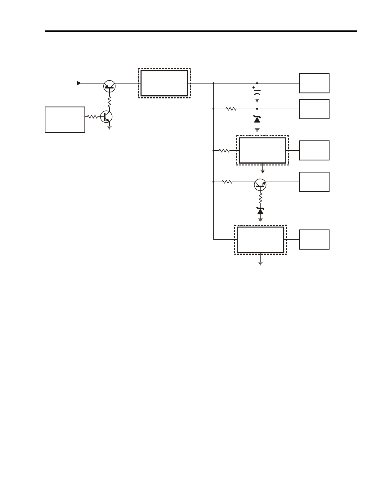
Run Supplies
There are several supplies generated from the main supply but only required during
run operation. They are shown in figure 2-17. To turn them on and off System
Control sends a high to Q14105-B turning it on. That turns Q14104 on passing the
+16Vs supply to the input of the main +12V regulator. The output of the regulator
then feeds +12V directly to the circuits or feeds other regulators.
28 Power Supply
T14401
10
6
2
FOCUS
SCREEN
4
To Beam
Limiter
9
8
5
7
R14701
10
1/2W 20%
CR14701
CR14704
R14703
0.88(0.82)
3W
CR14702
R14702
130K
1/2W
R14509
300
2W
10%
C14703
47uF
250V
R14508
1.0
2W 10%
FILAMENT
High Voltage
+
TO
CRT ANODE
TO
CRT FOCUS
GRID
TO
CRT SCREEN
GRID
+200Vr
+23Vr
+13Vr
TO
CRT
Figure 2-18, Scan Derived Supplies
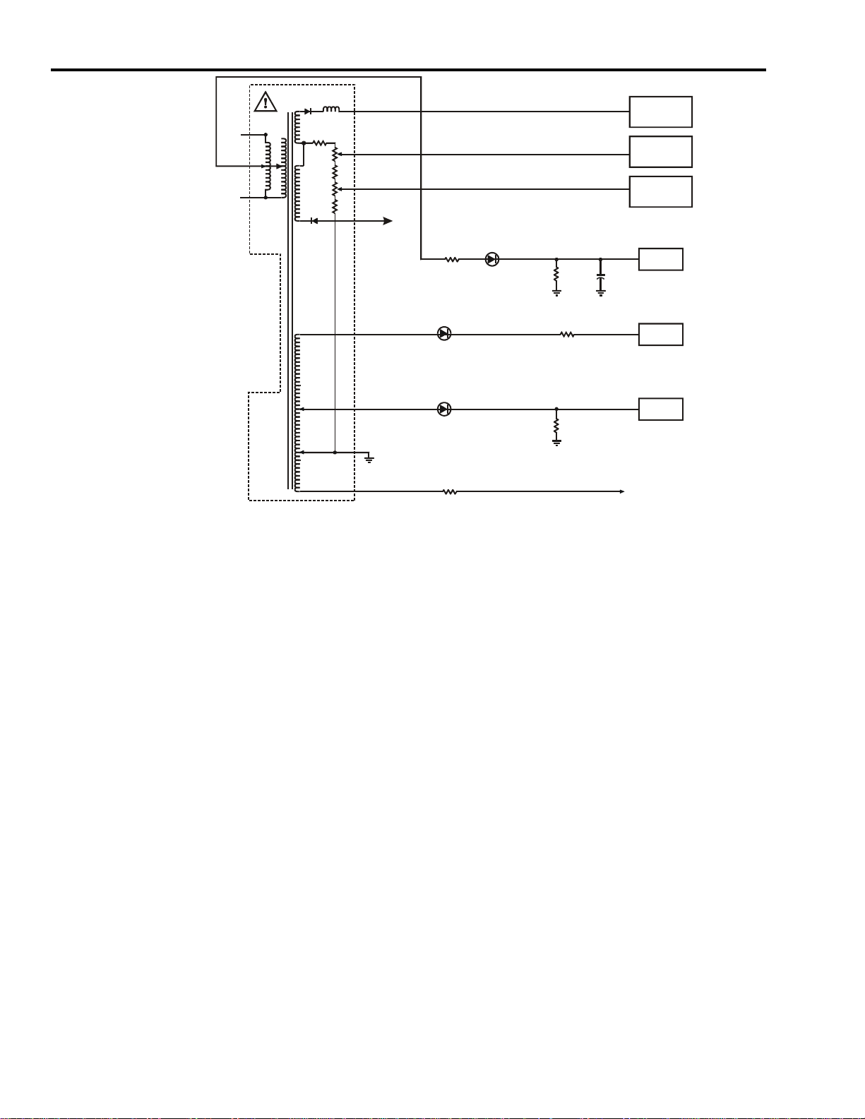
Scan Derived Supplies
Several other sources of power must also be generated by the CTC203. They are
derived from the scan circuits in a traditional way. Horizontal scan operation will be
covered later.
Two low voltage supplies are generated; +23V and +13V. An AC filament supply
for the CRT is taken from the same winding.
The CRT drivers require a higher voltage than can be generated by the normal
supply. It is generated here and is about +200V. It is slightly unique as it is derived
from the primary windings of the horizontal output transformer, not the secondary.
The remainder of the scan derived supplies are used to power and control the CRT.
They are the anode, focus grid and the screen grid supply.
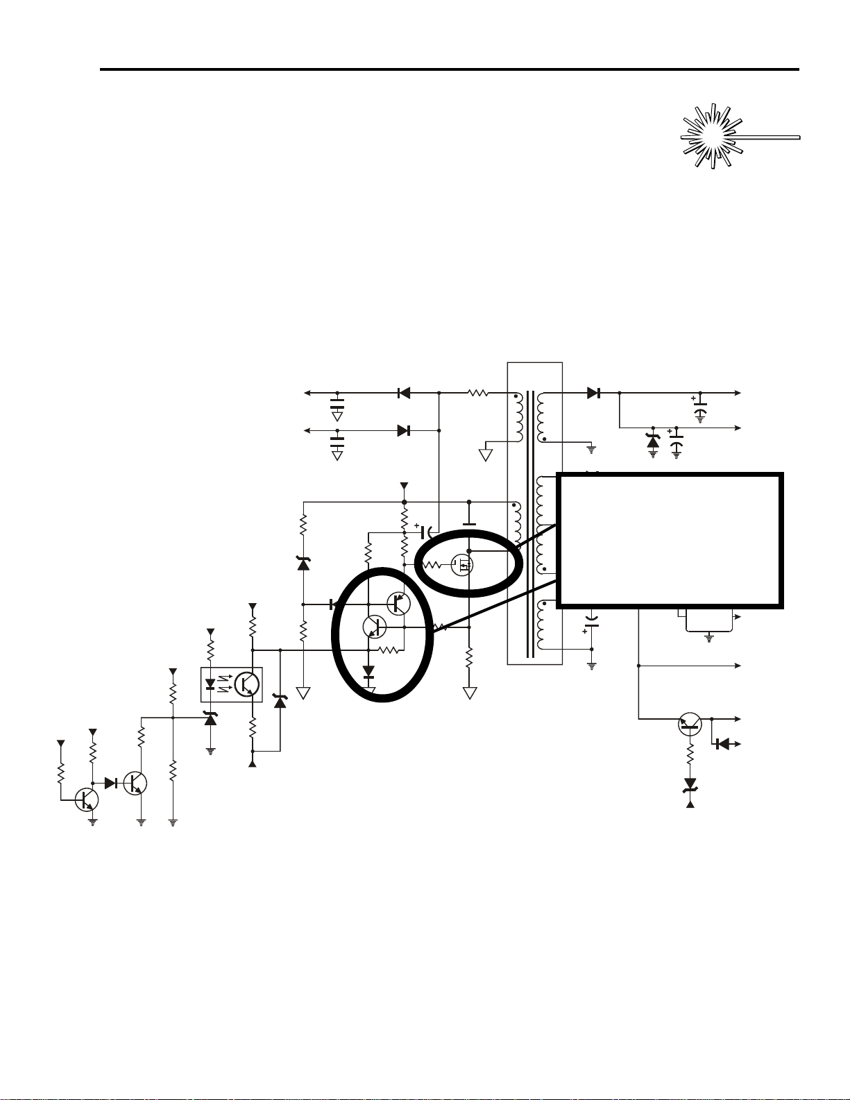
When output MOSFET Q14101 fails, it is a good idea to replace the latch transistors,
Q14102 & Q14103. Unexpected excessive current may damage these transistors
and other components in the immediate area.
Power Supply 29
TECH
TIP
+13Vr
R14128
680K
+16Vs
R14127
10K
CR14111
Q14107
R14115
143K
R14126
37.4K
Q14106
RegB+Vs
R14116
2000
+16Vs
R14113
1300
U14101
U14102
R14112
Bias Supply
Bias Supply
Pos Hot
Bias Supply
R141111
680
Neg Hot
Bias Supply
Pos Hot
Neg Hot
CR14101
47V
10K
CR14117
16V
R14101
47K
CR14102
R14102
6800
C14104
R14104
3300
Q14103
CR14105
0.047
C14108
0.047
CR14103
CR14104
R14103
1Meg
R14106
2000
R14110
22K
RAW B+
C14101
2.2uF
R14107
43
Q14102
R14109
750
R14105
10
C14108
1100
1.6KV
Q14101
R14108
0.1
3W
3
8
9
5
T14101
CR14106
16
C14122
33uF
C14114
3.3uF
L14102
C14122
33uF
R14124
3.3
2W
14
15
13
CR14107
33V
CR14108
C14121
3.3uF
Replace all on any
Reg B+
+33Vs
+16Vs
Output Device
R11513
4700
CR11504
18V
CR14110
U14103
Q11501
+12VrSW
+5.2V
Reg
CR11505
+7.6Vs
+5.2Vs
-12Vs
-12Vr
-12V
Fil
C14116
47uF
Failure
NC
10
11
12
Figure 2-19, Main Power Supply (Repeated)

30 Deflection
Deflection Overview
The CTC203 deflection circuits are very similar to previous TCE core line chassis.
Some models will have pin-corrected yokes, while others use an active pincushion
correction circuit. XRP is the same as previous chassis and other CRT control and
protection is also similar.
The horizontal deflection system has two primary functions in the CTC203 chassis.
First, it supplies the current for the horizontal yoke coils providing energy necessary
to move the electron beam horizontally across the face of the picture tube. Second,
it provides a number of voltage supplies needed for operation of the CRT and
deflection.
Horizontal yoke current is provided by a circuit consisting of a switch (HOT), the
primary inductance of the Integrated High Voltage Transformer (IHVT), a retrace
capacitor, trace capacitor (S-Shaping capacitor), and the horizontal yoke coils.
Voltage supplies provided by the horizontal deflection system are derived from
secondary and tertiary windings on the IHVT. The supplies are used by the video
amplifier (kine drivers), tuner, CRT, and the vertical amplifier.
Low level signal processing circuits for the horizontal deflection system are contained
in the T4-Chip. These include the horizontal sync separator and a two-loop horizontal
AFPC system. The T4-Chip allows bus control of several parameters associated
with the horizontal deflection system. These include horizontal drive pulse width,
AFC Gain, Sync Kill, and ON/OFF.
Enabling or disabling the horizontal drive signal from the T4-Chip determines
whether the chassis operates in the Standby or Run mode. In the Standby mode, no
IHVT-derived supplies are present reducing standby power requirements.
The vertical deflection circuit in the CTC203 is a linear amplifier DC coupled to the
vertical yoke coils. The circuit is similar to the CTC197 vertical circuitry. The
vertical ramp is generated in the T4-Chip. Vertical size, bias, S-Correction, and
linearity adjustments are done in the T4-Chip via the IIC bus. Timing information
for the ramp generator is derived from a digital vertical countdown circuit, resulting
in excellent interlace performance. The vertical output stage includes an integrated
circuit containing the power amplifier, vertical flyback generator, and thermal
protection.
 Loading...