


CTC175/176/177/186/187
Supplemental Training Manual
VERTICAL
TO
E8
RED BIAS
<21-B>
TO
E7
GRN BIAS
E5003
E5007
TP50
RED OUTP UT
194V
THO MSO N TECHNIC AL TRAINING
This training manual is a supplement to the CTC175/176/177 technical training manual (T-CTC175/
6/7-1). It contains additional information regarding system control circuit changes in later production
CTC175/76/77 chassis, new CTC186/87 circuits and an in-depth description of the tuner-onboard circuitry with troubleshooting strategies. This publication also contains "Tech Tips" from the
field on commonly encountered problems and their solutions. Using this manual in conjunction with
the CTC175/176/177 technical training manual and service data will enable the field technician to
repair these chassis more effectively and efficiently.
FOREWORD
Note: This publication is intended to be used only as a training aid. It is not intended to replace service
data. Thomson Consumer Electronics Service Data for these instruments contains specific
information about parts, safety and alignment procedures and must be consulted before performing
any service. The information in this publication is as accurate as possible at the time of publication.
Circuit designs and drawings are subject to change without notice.
SAFETY INFORMATION CAUTION
Safety information is contained in the appropriate Thomson Consumer Electronics Service Data. All
product safety requirements must be compiled with prior to returning the instrument to the consumer.
Servicers who defeat safety features or fail to perform safety checks may be liable for any resulting
damages and may expose themselves and others to possible injury.
All integrated circuits, all surface mounted devices, and many other semiconductors are electrostatically sensitive and therefore require special handling
techniques.
Prepared by
Thomson Consumer Electronics, Inc.
Technical Training Department
10330 North Meridian Street, Indianapolis, Indiana 46290-1024
U.S.A.

Table of Contents
CTC186/87 .................................................................................... 1
System Control .............................................................................. 4
MicroProcessoer Pinout .......................................................................................5
Comb Filter.................................................................................... 6
Troubleshooting .................................................................................................................................6
Stereo Decoder ..............................................................................7
dbx Alignments ..................................................................................................................................8
Inductor /Capacitor (LC) Basics .................................................... 14
Varactor Diode ................................................................................................................................15
Basic Tuner....................................................................................16
Oscillator / Mixer / IF Bandpass........................................................................................................ 17
PLL / Frequency Synthesizer............................................................................................................. 17
CTC176/77/86/87 Tuner ................................................................ 18
Single Tuned Filter ........................................................................................................................... 21
RF Amplifier.................................................................................................................................... 23
Double Tuned Filter.......................................................................................................................... 23
OSC., Mixer, PLL ...........................................................................................................................26
IF Amp ........................................................................................................................................... 29
Tuner Alignment ............................................................................................................................... 30
Troubleshooting ...............................................................................................................................31
Tuner Voltage Charts........................................................................................................................ 33
Tech Tips ..................................................................................... 41
Page 3
The CTC186/87 chassis is virtually the same as the CTC176/77 with the addition of a
dbx Stereo Decoder / Comb filter board. For complete descriptions of the common
circuitry, refer to the CTC175/176/177 Technical Training Manual (publication number
T-CTC175/6/7/-1).
CTC186/87
Later production CTC175/176/177 chassis have a different microprocessor (U3101).
These chassis can be identified with a “2” after the alpha suffix on the bar code label.
For example, a CTC177AA chassis that had the new version microprocessor would be
labeled CTC177AA2. This is extremely important because the pinouts are not the same.
In other words, they are NOT interchangeable. The CTC186/87 also supports this
newer version microprocessor.
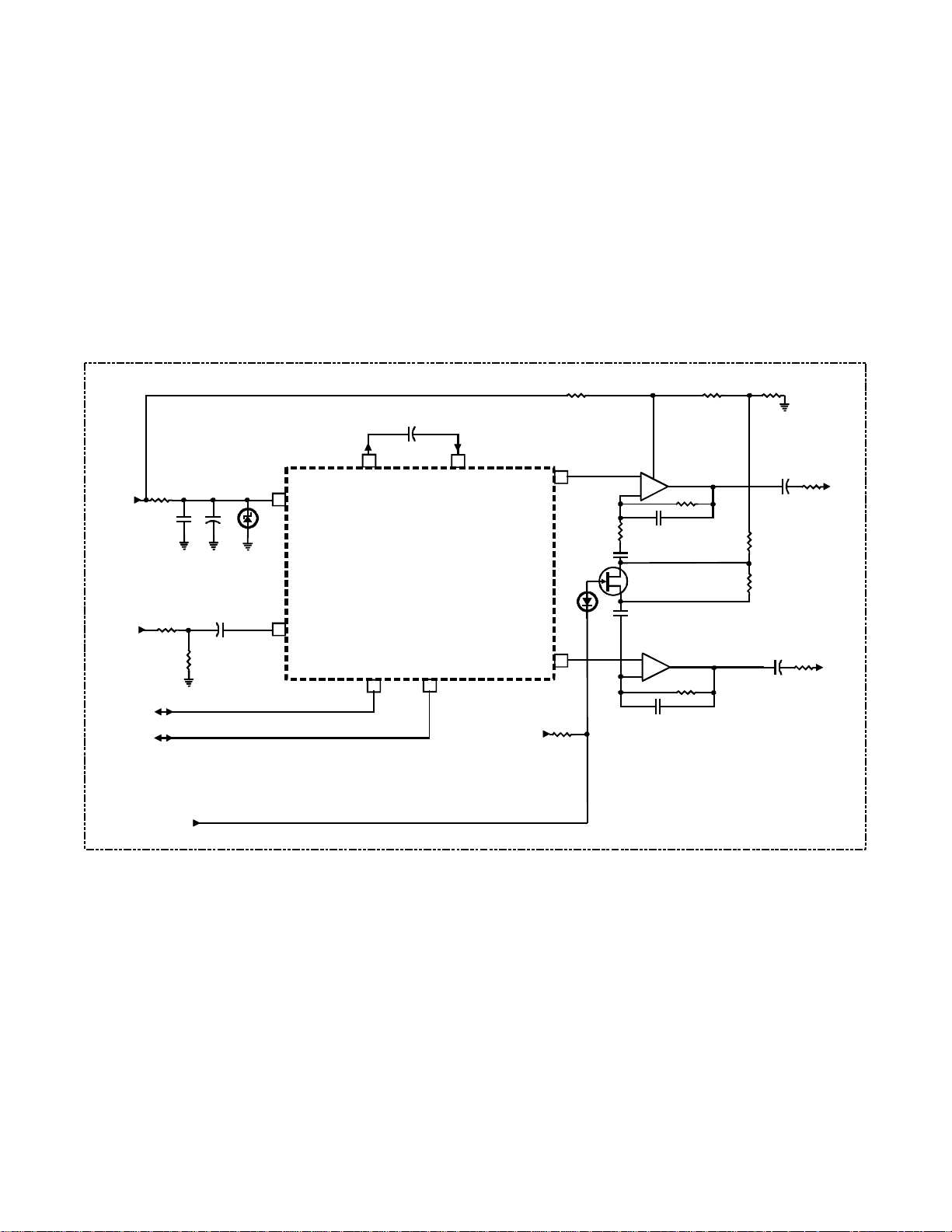
The use of the bus controlled stereo decoder (U1600) and the new Thomson ST-9
microprocessor (U3101), changes the system control block diagram slightly to accommodate the different parts. The differences are pin-out changes on the microprocessor
and the addition of U1600, figure 1. With the exception of these changes, the system
control circuit is functionally the same as the CTC177 (see the System Control section
of the CTC177 training manual).
POWER
VOL. UP
VOL. DN.
CH. UP
1,2, 3
GND
U3201
4,7
5V
KS1
6
KS2
7
KS3
8
KD1
5
T-CHIP DATA
TUNER CLOCK
T-CHIP CLOCK
TUNER DATA
U3101
µ
P
PIP
ENABLE
T-CHIP
ENABLE
8
19
20
12
14
EEPROM
VDD
DATA
5
CLO CK
6
DATA
20 21
U2901
D-PIP
CLOC K
GND
VDD
ENABLE
22
39
54
53
52
System Control
3,5
15, 16
40, 41
5V
DATA
CLOCK
U1001
T-CHIP
ENABLE
HORZ.
OUT
24
CH. DN.
MENU
5V
2
IR3401
3
5V
2
RESET
VDD
21
OSC
OSC
GND 56
1
OUT
36 37
1
Y3101
22
IN
4
DATA
CLOCK
5V
5
U7401
5V
TUNER PLL
VCC
10
GND
13
7.6 V
STBY
9V
CTC186/87 ONLY
22
STEREO DEC OD ER
VCC
15
BUS
GND
1
DATA
U1600
2
CLOC K
GND
3,4,
17
Figure 1, System Control Block Diagram
Page 4
U3101 - Thomson ST-9 SYSTEM CONTROL MICROPROCESSOR
PIN NO. NAME VOLTAGE
1 IR IN 4.5
2 RESET 5
3 NC 4 DEGAUSS 0
5 KD1 0
6 KS1 4.7
7 KS2 4.7
8 KS3 4.7
9 DATA OUT 0.3
10 ATE ENABLE 0
11 CC VIDEO 2
12 PIP ENABLE 4.7 >20M
13 NC -
14 T-CHIP ENBL 4.6 >20M
15 BLUE OSD 0
16 GRN OSD 0
17 RED OSD 0
18 FSW 0
19
20
T-CHIP DATA
TUNER/ST CLK
T-CHIP CLK
TUNER/ST DATA
4.5
4.7 >200K Serial communication - data/clock
21 VDD 4.7
22 VSS 0
23 PLL FILTER 2.6
24 PLL BIAS 2.2
25 PLL VCC 4.7
26 H 0.7
27 V 0.2
28
EXP S T SW
ST / MONO
11 / 0 36K Expanded stereo, NWS-gain and mono /stereo control line.
29 SPK MUTE 0
30 TONE 0 / 5
31
SCLOCK/FM
ON/OFF
0 >20M
32 ST SENSE 0 / 5
33 RF SEC * VARIES >20M
34 RF PRI * VARIES >20M
35 SINGLE TUN * VARIES
36 OSC OUT 2.3
37 OSC IN 2.3
38 TUN SYNC 2.3 >20M
39 FM TUN * VARIES
40 IF DEFEAT 0
41 STBY SW 42 DATA IN 4.8
IN CKT. RES.
>300K
>200K
>20M
>20M
>200K
>200K
>200K
>20M
10K
>50K
-
1K
1K
1K
2K
>20M
>20M
0
>20M
6K
>20M
8K
1.8K
>100K
>100K
>20M
>20M
>20M
>20M
>20M
>20M
>20M
>200K
Serial communication line used to control data between
the micro. and PIP.
Serial comm. line used to control communication between
the micro and T-Chip.
Fast switch - controls OSD and video switching in T-chip.
Serial clock for DBX stereo decoder. FM on control for
commercial TV.
PWM output - Controls the secondary of the double tuned
filter in the tuner.
PWM output - Controls the primary of the double tuned
filter in the tuner.
PWM output - Controls the single tuned filter in the tuner.
Sync input to detect the presence of an active channel
when tuning.
Input to detect an active FM station on commercial TV.
Page 5
DESCRIPTION
IR input signal from remote control.
Micro reset - active LO.
-
Activates degaussing relay.
Keyboard drive line.
Keyboard scan input.
Keyboard scan input.
Keyboard scan input.
Data out for commercial television.
Used for factory testing.
Closed caption video input.
-
Blue OSD output.
Green OSD output.
Red OSD output.
Serial communication - data/clock.
Power supply input for microprocessor.
Ground for microprocessor.
PLL filter network.
PLL bias resistor Connection.
Power supply for PLL.
Horizontal timing input for OSD.
Vertical timing input for OSD.
Goes HI to mute speakers.
Goes HI for low tone and LO for high tone.
Stereo Detect line for non-DBX stereo sets.
8MHz crystal connection.
8MHz crystal connection.
Output to defeat IF circuit via AGC.
-
Data input for commercial television.
This board contains an analog comb filter that is used to separate luminance and chrominance. Composite video is routed from the main board from E2601 and applied to the
input at pin 2 of the comb filter IC (FL2651). Luma is output at pin 5 and chroma is
output at pin 3. These signals are sent back to the main board at E2602 and E2603
where they are input to the T-Chip (U1001), figure 2. Refer to the luminance and
chrominance processing section of the CTC177 training manual for signal processing on
the main board.
+12V
Q2651
+9V
+
Comb Filter
E2505
GND
1
5
E2601
VIDEO IN
2
FL2651
3
4
STEREO DECODER / COMB FILTER PCB
Figure 2, Comb Filter
1. Check for composite video at E2601. If there is no video present, the problem is on
the main board and not the comb filter. If video is present, go to the next step.
2. Check for luma and chroma out at E2602 and E2603. If luma and chroma are
present, the comb filter is working correctly. If they are not present, go to the next
step.
E260 2
LUM A OUT
E260 3
CHROMA OU T
Troubleshooting
3. Check for 9 volts at pin 1 of the comb filter (FL2651). If the voltage is present,
suspect a defective FL2651. If the voltage is missing, check Q2651 and its associated components.
Page 6
Stereo Decoder
The stereo decoder (U1600) receives wideband audio from the main board and decodes left and right audio information. Wideband audio enters the board at JS107
(figure 3) and is capacitively coupled to U1600 pin 11. Decoded left and right signals
are output at pins 29 and 28 respectively. U1601 buffers the left and right output and
provides the expanded stereo feature in conjunction with Q1601. When the expanded
stereo line (JS112) goes LO, Q1601 turns on and cross-mixes the left and right channel
information to produce a perceived increase in stereo separation. Pins 1 and 7 of U1601
output the left and right signals respectively that are capacitively coupled back to the
main board via JS105 and JS106.
+12V
JS103
WBA
JS107
SCLK
JS111
SDATA
JS110
EXP. STEREO
JS112
+
CR1600
9.1V
+
15
11
VCC
WBA IN
8 7
MAIN
OUT
MAIN
IN
U1600
STEREO DECODER
2 1
STEREO DECODER / COMB FILTER PCB
L OUT
R OUT
+12V
29
CR1601
28
U1601
3
2
Q1601
U1601
5
6
8
+
1
-
+
7
-
+
+
LEFT
JS105
RIGHT
JS106
Figure 3, DBX Stereo Decoder
Page 7
U1600 is digitally controlled over the I2C bus. Analog lines that were used in the
CTC177 for stereo sense and stereo select (see the Audio Processing section of the
CTC177 training manual) are no longer used. Instead, communications between U1600
and the television’s microprocessor are carried out over the serial bus, figure 4.
U1001
T-CHIP
AMP
AMP
BUS
CTL
VOL ./M UTE
BUS CTL
WB AUDIO
OUT
L INR IN
4
5
3
60
C1912
59
Q1901
C1913
R1912
Q1902
+
5
+
1
+
3
AUX LEFT
AUDIO INPUT
AUX RIGHT
AUDIO INPUT
+
7
+
8
AMP
AMP
U1901
8
9
10
6
LEFT HI-FI
OUT
R / MO NO
HI-FI
OUT
LEFT
26V
RIGHT
Q1903
MUTE
R1913
29
30
20
19
29
28
R OUT
TV
AUDIO
L OUT
11
WB AUDIO
IN
U1600
ST EREO
DECODE R
STEREO DECODER / COMBFILTER PCB
SCLK
SDATA
1
2
Figure 4, Audio Circuit Block Diagram
The CXA 1734S Stereo/SAP Mpx IC registers are accessed via the IIC Bus. All
necessary bus controls are contained in the SERVICE MENU.
Signal Description Summary
ALIGNMENT INPUT SIGNAL DESCRIPTIONMEASUREMENT
WBA Input;JS107
#25 ATT 100 Hz, 424 mv rms JS106 (RIGHT OUT)
#26 STVCO Open WBA or short AC to gnd. JS106 (RIGHT OUT)
#27 SAPVCO 78,670 Hz (5 x fH), 255 mv rms Observe OSD * (star)
#28 STLPF 9.4 KHz, 1.04 v rms Observe OSD STEREO”
#29 SAPBPF 88 KHz, 206 mv rms Observe OSD * (star)
#30 WBSEP Stereo, LEFT only, 300 Hz w/ pilotJS106 (RIGHT OUT)
#31 SPECSEP Stereo, LEFT only, 3KHz, w/ pilot JS106 (RIGHT OUT)
SPEAKR
MUTE
TONE
SCLK
SDATA
U310 1
SYSCON
dbx Alignments
Page 8

NOTES:
• All replacement stereo IC’s must be aligned according to this procedure.
• All Stereo/SAP alignments must be performed in the sequence shown. Several
alignments are coarse alignments for ones that follow.
• When the set starts up, the dbx Stereo IC will be aligned with IIC alignment data
which is stored in EEPROM memory from the previous IC that was installed in the
set. In most cases, stereo and SAP will be detected, but the stereo and SAP vco
free-running frequencies will not be properly aligned. Neither will stereo separation
nor the various internal filters be optimized. The full alignment procedure must be
performed to make sure the IC performs within specification.
• A modulator or other signal source with video must be connected to the tuner, and
the set tuned to the appropriate channel in order to detect stereo. Stereo and SAP
alignments cannot be performed with VIDEO IN selected (channel 00).
Alignment Preparation
Make sure that the EXPANDED STEREO function is turned off, otherwise the output
amplitudes will be in error. Also, STEREO SEPARATION alignments will be impossible.
Access the SERVICE MENU for the dbx IC as follows:
1. Press and hold the MENU button, then while holding MENU press the ON button,
followed by the VOLUME + button. This accesses the GENERAL SERVICE
MENU display.
2. Release all buttons.
3. Increment VALUE (V) number to 76 by pressing and holding the VOLUME UP
button.
4. Increment PARAMETER (P) number to 13 by pressing and holding the CHANNEL
UP button.
5. Increment V number to 77 with VOLUME UP button.
6. Increment P number to 25 with CHANNEL UP button. This is the first alignment
parameter.
Page 9

Perform the alignments in the following sequence.
Attenuator (ATT = Parameter # 25)
DAC range = 0 to 15.
All following alignments depend on the correct setting of this alignment.
1. Unsolder and lift the bottom end of R1609 from the circuit board. This is the
Wideband Audio input (WBA) to the CXA1734 stereo IC.
2. Connect an audio generator to the unsoldered end of R609 (WBA). Adjust the
generator output for 100 Hz, 424 mv rms, +/- 10 mv at module pin #7, WBA. This
corresponds to a full 25KHz carrier deviation mono audio signal from the sound IF.
3. Connect an AC voltmeter to module JS106, RIGHT CHANNEL OUTPUT. This is
also the bottom end of R612. (Do not use the top end, or oscillations may result.)
Adjust the ATT DAC using the volume control button. Set the DAC for an output
level as close to 489 mv rms as possible. Each DAC step will change the output
level by about 25 mv.
4. Observe on an oscilloscope that the audio output at module pins #5 (LEFT) and #6
(RIGHT) are clean and undistorted.
5. Observe that the rms amplitude of both pins #5 and #6 are within 20 mvrms of each
other.
6. If the final DAC alignment value is not within the range of 7 - 11, check to make
sure that the signal amplitude is proper. (Do not use 1KHz, because the internal deemphasis filter will cause an amplitude error.)
STEREO VCO free running frequency. (STVCO = Parameter # 26)
DAC range = 0 to 63.
This alignment is also a course adjustment for the next alignment.
1. Remove the audio generator connection from the bottom end of R1609. False
STVCO frequency will be generated if WBA is not open, as VCO tries to lock to
noise or other frequency.
2. Connect a frequency counter to module JS106, RIGHT OUT. (4 x fH vco is
automatically routed to JS106 when in P#26.)
3. Adjust DAC while monitoring frequency. Set DAC for frequency = 62,936 Hz +/200Hz. (4 x fH). The frequency increment for each DAC step is approximately 300
Hz.
Page 10

SAPVCO free running frequency. (SAPVCO = Parameter # 27)
DAC range = 0 to 15.
This is not a direct frequency measurement. It uses the internal status registers of
the stereo IC to indicate PLL lock. The previous alignment (STVCO) is a coarse
adjust for this alignment.
1. Adjust audio generator for 78.67 KHz, 254 mv rms (559 Vp-p), +/- 10 mv. (5 x
fH SAP subcarrier, equivalent to 15 KHz carrier deviation) at WBA input.
2. Set SAPVCO DAC to step # 0. Observe TV screen. No star (*) should be
present.
3. Increment DAC once per second or slower until * becomes present. Record this
DAC setting. (A flashing * is OK. Usually, one more DAC increment will stop the
flashing.)
4. Set DAC to step # 15. Observe that no * is present. Decrement DAC until * once
again becomes present. Record this DAC setting.
5. Average the DAC settings from steps (c) and (d). Set DAC to this averaged value.
This is the proper alignment value for SAPVCO. Setting will usually be 1 - 14. If
not, verify that previous step was done properly.
STEREO LOWPASS FILTER (STLPF = Parameter # 28)
DAC range = 0 to 63.
This alignment is also a course adjustment for the next alignment.
1. Adjust audio generator for 9.4 KHz, 1.04 vrms (1.47 Vp-p) at WBA input.
2. Set STLPF DAC to step # 0. Observe TV screen. No “STEREO” indicator
should be present.
3. Increment DAC once per second or slower until “STEREO” indicator becomes
present. Record this DAC setting. (It is OK for the “STEREO” indicator to flash.
Usually, one more DAC increment will stop the flashing.)
4. Set DAC to step # 63. Observe that no “STEREO” indicator is present. Decrement DAC until “STEREO” indicator once again becomes present. Record this
DAC setting.
5. Average the DAC settings from steps (c) and (d). Set DAC to this averaged value.
This is the proper alignment value for STLPF.
Page 11

SAP BANDPASS FILTER (SAPBPF = Parameter # 29)
DAC range = 0 to 15.
1. Adjust audio generator for 88 KHz, 220 mv rms, +/- 10 mv.
2. Set SAPBPF DAC to step # 0. Observe TV screen. No * should be present.
3. Increment DAC once per second or slower until * becomes present. Record this
DAC setting.
4. Set DAC to step # 15. Observe that no * is present. Decrement DAC until * once
again becomes present. Record this DAC setting.
5. Average the DAC settings from steps (c) and (d). Set DAC to this averaged value.
This is the proper alignment value for SAPBPF.
WIDEBAND SEPARATION (WBSEP = Parameter # 30)
DAC range = 0 to 63.
This alignment is for the dbx WIDEBAND detector
1. Set stereo generator for STEREO LEFT CHANNEL ONLY SIGNAL, 300 Hz.
2. Connect AC rms voltmeter to module JS106, RIGHT CHANNEL OUT.
3. Set WBSEP DAC to step # 31 (DAC midpoint).
4. Start incrementing WBSEP DAC (or decrementing, as necessary) while observing
voltmeter reading. Find DAC setting which produces a minimum voltmeter reading
(null setting). Record this DAC setting. The exact null setting will typically be
difficult to determine, because the null range is rather broad.
5. Measure module JS105, LEFT CHANNEL OUT, and check for at least 20 dB
separation between LEFT and RIGHT.
6. This alignment will be repeated after doing the next alignment, because of some
interaction between the WBSEP and SPECSEP DAC’s.
Page 12

SPECTRAL SEPARATION (SPECSEP = Parameter # 31)
DAC range = 0 to 63.
This alignment is for the dbx SPECTRAL detector
1. Set stereo generator for STEREO LEFT CHANNEL ONLY SIGNAL, 3KHz.
Note:If the MTS generator being used is not capable of generating a 3KHz signal,
the alignment cannot be performed. If this is the case, set the DAC to the nominal
default of 35.
2. Connect AC rms voltmeter to module JS106, RIGHT CHANNEL OUT.
3. Set SPECSEP DAC to step # 31 (DAC midpoint).
4. Start incrementing SPECSEP DAC (or decrementing, as necessary) while observing
voltmeter reading. Find DAC setting which produces a minimum voltmeter reading
(null setting). Record this DAC setting. The exact null setting will typically be
difficult to determine, because the null range is rather broad. Do the best you can.
5. Measure module JS105, LEFT CHANNEL OUT, and check for at least 20 dB
separation between LEFT and RIGHT.
Page 13
A television tuner receives (or selectively tunes) a 6MHz bandwidth RF (Radio Fre-
N
quency) carrier that contains audio and video information and converts it to a common IF
signal (Intermediate Frequency). The IF signal is demodulated by the television into its
audio and video components. All tuners work on the principle of a tuned circuit whose
resonant frequency determines what channel is tuned. By changing the tuned circuits’
resonant frequency, different RF carriers (channels) are selected. Before discussing the
different sections that comprise the tuner’s circuitry, it is appropriate to review certain
fundamental concepts of inductors, capacitors and varactors. These components play a
major role in all tuned circuits.
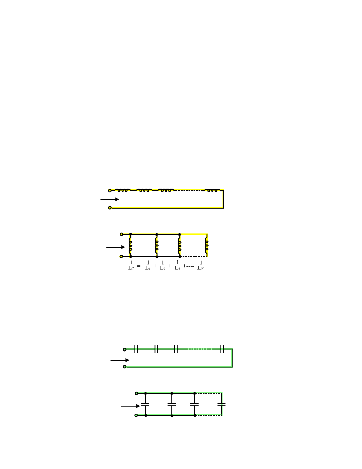
Inductors
Remember, an inductor is simply a coil of wire. The ability of a coil to oppose a change
in current is a measure of the inductance L of the coil. Inductance is measured in henries
(H). For inductors in series, the total inductance is found in the same manner as resistors
in series, figure 5. Likewise, the total inductance of inductors in parallel is found in the
same manner as resistors in parallel, figure 5. The main idea to remember here is inductors added in parallel reduce the total inductance and inductors added in series in-
crease the total inductance.
Inductor /
Capacitor
(LC) Basics
1
T
L
L
T
L
2
L
3
L
LT = L1+L2+L3+- -- -L
1
L
2
L
N
3 L
L
N
L
N
Figure 5, Inductors in Series and Parallel
Capacitors
Capacitors are components that are made up of two parallel conducting plates separated
by an insulating material. A capacitor stores a charge on its plates. The storage capacity
C is measured in Farads (F). The farad is generally too large a unit for most tuner
applications so the pico farad (pF) 10
-12
F is used. Total capacitance is calculated in
the opposite manner as inductance, figure 6. Capacitors in parallel increase total
capacitance and capacitors in series decrease total capacitance.
C T
C
1
C
C
2
3
C
N
1 1 1 1 1
= + + + − − −
1 2 3
T
C C C C C
T
C
C
1
CT = C1+ C2+ C3+ --- - C
C
2
N
C
3
N
C
Figure 6, Capacitors in Series and Parallel
Page 14

These two fundamental concepts are essential to understanding and troubleshooting tuner
circuits. The circuit in figure 7 is a simple parallel resonant band-pass filter circuit, similar
to what would be found in a tuner. The frequency is determined by relationship as
shown. The main point here is decreasing the capacitance and/or inductance will
raise the resonant frequency. Increasing the capacitance and/or inductance will
lower the resonant frequency.
Vi
+
L
-
+
C
Vo
-
Vi
fp
f
1
fp
=
π
2
Figure 7, Band-pass Filter
Varactor Diode
One of the major components that is found in an electronic tuner is the varactor diode.
The varactor acts like a voltage variable capacitor. An increase in reverse bias across
the diode causes the capacitance to decrease. Conversely, a decrease in reverse bias
causes its capacitance to increase. This allows the resonant frequency of a tuned
circuits to be change by applying a tuning voltage, figure 8.
LC
SIGNAL
SOURCE
TUNING VOLTAGE
SOURCE
Figure 8, Basic Varactor Tuning Circuit
Page 15
Input Filter
A tuner is composed of the basic elements shown in figure 9. The front end of a tuner
has a filter network that filters out unwanted FM and IF frequencies that may be present.
It also contains a singled tuned filter that tunes the frequency of the desired channel and
inputs this signal to the RF amplifier.
Basic Tuner
ANTENNA
INPUT FILTER
RF AMP
CHANNEL 6
PIX = 83.25MHz
RF BANDPASS
OSCILLATOR
B+AGC
83.25MHz S 129MHz =
MIXER
129 MHz
OSC. NETWORK
SUM 212.25MHz
IF BANDPASS
Figure 9, Basic Tuner
RF Amplifier
The RF amplifiers in the tuners we will be concerned with use dual gate depletion type
MOS FET’s (Metal Oxide Semiconductor Field Effect Transistors). These transistors
are very high impedance (in the mega ohms) voltage controlled devices that function
very much like vacuum tubes. The N-channel depletion type MOSFET’s are normally
“on” without any type of gate bias. When a negative voltage is applied to the gate with
respect to the source, drain current flow is reduced or pinched off entirely if the reverse
bias is sufficient. Conversely, a positive voltage on the gate with respect to the source
will increase drain current flow to a point. Dual gate MOS FET’s have two gates both
of which affect drain current. In RF amplifier configurations, the RF signal is input on
Gate 1 and the AGC (Automatic Gain Control) voltage is applied to Gate 2. As the
AGC voltage rises, more drain current is produced increasing the output of the respective RF stage. As the AGC voltage decreases, the output of the RF stage decreases.
These fundamental principles are important when troubleshooting.
DIFF. 45.7 5MHz
IF PIX = 45.75MHz
IF
RF Bandpass
The RF bandpass is a double-tuned filter that receives the amplified signal from the RF
amplifier and re-tunes it. This performs “sharp” tuning of the RF signal to obtain greater
selectivity. It also performs some impedance matching to the latter stages of the tuner.
Page 16

Oscillator / Mixer / IF Bandpass
E
The oscillator network comprises the local oscillator with its control circuitry. The
oscillator generates a signal that is beat or heterodyned against the incoming RF signal.
This is done to obtain the IF picture frequency of 45.75MHz. To accomplish this, the
oscillator frequency is set 45.75MHz higher than the incoming RF signal. The two
signals are “beat” or heterodyned together in the mixer stage. Using channel 6 as an
example, the picture frequency of 83.25 MHz is heterodyned with an oscillator frequency of 129MHz. This produces a sum signal of 212.25MHz and a difference signal
of 45.75MHz. The IF bandpass extracts the difference signal which produces the
channel’s video carrier at 45.75 MHz, the chroma carrier at 42.17MHz and the audio
carrier at 41.25MHz. Changing the local oscillator frequency accordingly allows all
channels to produce the same IF frequencies.
PLL / Frequency Synthesizer
The local oscillator frequency must change over a wide range to convert the many
channels to the IF frequency. The local oscillator in modern electronic tuners, and more
importantly the tuner in the CTC175/76/77/86/87 chassis, uses a frequency synthesizer
to control the oscillator. A frequency synthesizer is made up of a PLL (Phase Lock
Loop) and a programmable divider circuit.
A basic PLL block diagram is shown in figure 10. A voltage controlled oscillator (VCO)
sends a frequency sample back to a comparator. The comparator compares the sample
frequency of the oscillator to a reference signal derived from a crystal controlled oscillator. When the oscillator is off the frequency, the comparator generates an error voltage
that corrects the oscillator. The VCO will stay locked to the reference oscillator.
FREQUENCY
SAMPLE
VOLTAGE
CONTROLLED
OSCILLATOR
FREQUENC Y
COMPARATOR
REFER ENCE
FREQUENCY
CRYSTAL
CONTROLLED
OSCILLATOR
Figure 10, Basic Phase Locked Loop (PLL)
Page 17
DC VOLTAG

Adding a programmable divider to the PLL enables the oscillator to be locked at differ-
CTC176/77/86/87
E
ent frequencies. Division logic, usually supplied by a microprocessor, sets a divide ratio
in the frequency divider. The divided down frequency is compared against the reference
frequency. The comparator generates a correction voltage to keep the oscillator locked
to the desired frequency, figure 11. By changing the frequency divider, the PLL is able
to “synthesize” different frequencies.
VOLTAGE
CONTROLLED
OSCILLA TOR
FREQUENCY
COMPARATOR
REFERENCE
FREQUENCY
CRYSTAL
CONTROLLED
OSCILLATOR
DIVISION
LOGIC
FREQUENCY
SAMPLE
FREQUENCY
DIVIDER
(÷N)
FREQUENCY
SAMPLE
÷
N
DC VOLTA G
The CTC176/177/186/87 chassis supports a new concept in tuner design. The tuner is
built on the main board instead of being a separate assembly. This change will require
the technician to repair the tuner instead of replacing it. Although repairing the tuner may
be new for some, it is no different than working on other discrete sections of the TV.
Figure 11, Frequency Synthesizer
Tuner
Page 18

The tuner on board is digitally aligned. The television microprocessor adds offset voltage
T
to the single tuned and primary and secondary of the double tuned circuits. This allows
the three stages of the tuner to be independently adjusted to optimize circuit performance
for each channel. This improves the tuners overall response on cable systems as well as
off-air signals, figure 12.
LOW PASS
FILTER/SUMMING
U3201
EEPROM
SINGLE
TUNED FILTER
ST. P WM
BAND
SW
U7501
PRI. P WM
RF
AMP
BAND
SW
U3101
P
DOUB LE
TUNED FILTER
PRI. SEC.
BT BTBT
BAND
SW
SEC. PWM
BAND
SW
MIX ER
LO
BT
IIC BUS
FROM
P
IF FI LTER
U7401
TUNER
PLL
IF
OU
BAND
SW
Figure 12, CTC176/77/86/87
When a channel is selected, U3101 sends clock and data information to U7401 telling it
what band and frequency to synthesize. The output of pins 1 and 14 of U7401 sets up
the tuning voltage for the local oscillator (VT/LO) and the VREF tuning voltage. The
VT/LO tuning voltage adjusts the frequency of the local oscillator to produce the IF
frequency of the desired channel. A sample of the local oscillator's frequency is fed back
to U7401 pin 11 to serve as feedback for the phase lock loop (digital AFT information is
also fed to U3101 from U1001 over the serial bus which in turn adjusts U7401). The
band switching voltages from U7401 pins 8 and 9 tell the filters what band to tune. At
the same time, the VREF tuning voltage is summed with D/A voltages from U3101 and
sent to the single and double tuned filters to tune the desired channel’s RF carrier, figure
12. The D/A levels are set via digitally stored alignment data.
Page 19

W
R
ANT
U/V SPLIT
B3 ST.
FM & IF
TRAPS
INTERFACE CIRCUIT
RESPONSE
30
RF
TUNING
VOLTAGE
0
LO TUNING
VOLTAGE
Q7101
UHF
AMP
R7101
R7109
AGC
B1/B2
V ST.
VHF
AMP
Q7102
BS1
R7520
R7519
8 14 7
V ST. V PR I. V SEC.
U7501
INTERFACE C IRCUITRY
D/A STEP 63
D/A STEP 0
30
LO
TUNING
VOLTAGE
B3 DOUBLE TUNED
V PRI.
BV/U
RF
BV/U
B1/B2 DOUBLE TUNED
V PRI. V SEC.
BS1
VREF
3
V SEC.
R7518
BV/U
7
VHF/UHF
12
10
1ST IF
FILT ER
5
3
4
8+ 12V
U3101
D/A SEC.
34
5
12
35
36
10
D/A PRI.
D/A ST.
SYSTEM
CONTROL
UHF
M IXER
VHF
MIXER
U7301
OSC./M IX
15
16
AMP
OSC.
IF
UHF
VHF
OSC.
BS 1
CLOCK
DATA
B3 OSC
16
TANK
2ND IF
1
FILT ER
FM SAW
OUT PUT
9
B1/B2
OSC TANK
8
BS 1
5
U7401
TUN ER
4
65
VREF
U3201
EEPROM
RESISTIVE
DIVIDER
+ 5V
PLL
10
BV/U
9
fLO
SAW
AMP
11
1
14
R7301
fLO
fLO
BV/U
fLO
VT/LO
VT/LO
VT/LO
SPLIT
VT
TO SA
FILTE
TO FM
SIP
VT/LO
+33V
Figure 13, Tuning Circuit Block Diagram
The alignment data for the channels is stored in U3201, the EEPROM, and is used by
U3101, the microprocessor, during channel selection, figure 13. Pins 34, 35 and 36 of
U3101 output a PWM (pulse width modulated) signal that is low pass filtered and
summed in U7501 with the VREF (voltage reference) from the PLL circuitry. These
voltages control the secondary and primary of the double and the single tuned filters
respectively. The actual voltage to the filters is a function of the tuning voltage from the
local oscillator plus a correction voltage from the D/A’s of U3101.
U7501 forms the interface circuit that low pass filters the PWM signal from U3101 and
sums it with the VREF tuning voltage. The interface circuit response is shown on figure
13. The higher the tuning voltage, the more offset voltage range from the D/A’s. This is
necessary because varactor diodes require more voltage across them to get the same
change in capacitance at higher tuning voltages than at lower tuning voltages.
Page 20

RF from the antenna connector is passed through a trap network to remove any FM or
F
F
IF signals that might have been picked up by the antenna. The filtered RF is then tuned
by the single tuned filter. The circuit shown in figure 14 is the VHF single tuned filter.
The VHF low band channels (2 - 6) span frequencies from approximately 54MHz to
88MHz. The VHF high band channels (7- 13) and the midband cable channels (A - I)
span frequencies from approximately 120MHz to 212MHz. There is an approximate
32MHz gap between the VHF high and low bands that makes it impractical for a single
varactor circuit to tune. Therefore, inductors are added to the circuit with switching
diodes to cover this range of frequencies.
RF
IN
FM/IF
TRAP
C7140
C7142
L7108
C7110
CR7112 CR7105
R7112
R7138
BS1
L7115
C7134
PCBL1
L7107 CR7106
CR7107
L7106
R7114
C7137
SINGLE_TUNED
C7113
TO R
AMP
R7113
Figure 14, CTC175/76/77/86/87 VHF Single Tuned Filter
In the case of VHF low band channels, BS1 is set to approximately -14.5 volts. This
reverse biases CR7112 and CR7105. The inductors that make up the tuned circuit are
L7108, L7115, L7107 and L7106, figure 15. The inductors are tuned by the
SINGLE_TUNED voltage applied to varactors CR7106 and CR7107. This voltage is
affected by the digital alignments but is normally around 0 volts for channel 2 and around
5 volts for channels 6.
RF
IN
FM/IF
TRAP
C7140
C7142
L7108
C7110
CR7112 CR7105
R7112
R7138
BS1
L7115
C7134
PCBL1
L7107 CR7106
CR7107
L7106
R7114
C7137
SINGLE_TUNED
C7113
TO R
AMP
R7113
Figure 15, Single Tuned Filter (BS1 = -14.5V)
Page 21

In the case of VHF high band channels, BS1 is set to approximately +11.5 volts. This
F
turns on CR7112 and CR7105. With CR7112 turned on, L7108 is shunted, removing it
from the circuit. CR7105 connects PCBL1 to the circuit in parallel with L7106. This
switching action reduces the total inductance allowing the higher frequencies to be tuned
by CR7106 and CR7107, figure 16. The SINGLE_TUNED voltage will vary from
approximately 0 to +30 volts depending on the band and channel being tuned. The
higher the voltage, the higher the frequency being tuned.
L7107 CR7106
CR7107
L7106
R7114
C7137
SINGLE_TUNED
RF
IN
FM/IF
TRAP
C7140
C7142
L7108
C7110
CR7112 CR7105
R7112
R7138
BS1
L7115
C7134
PCBL1
Figure 16, Single Tuned Filter (BS1 = +11.5)
The BS1 line is switched positive (approximately +11.5) for cable channels 7- 13,
and 18 - 125. The BS1 line is switched negative (approximately -14.5) on cable
channels 2 - 6, and 14 - 17.
C7113
TO R
AMP
R7113
TECH
TIP
The UHF single tuned filter is analogous to the VHF circuit with one exception. The
frequencies tuned by the UHF circuitry are contiguous (no large gaps like VHF) so
inductor switching is not performed.
Page 22

The tuned “channel” from the single tuned filter is sent to the RF amplifier (Q7102) G1
T
through C7113. The ACG voltage is applied to G2, figure 17. The higher the AGC
voltage the higher the gain of the RF stage. Q7403 and Q7404 make up the VHF/UHF
switch. When a VHF channel is selected, the switch is turned on providing a ground
path for the source of Q7102. When the UHF RF circuitry is used, the BV/U switch is
turned off, removing the ground path from Q7102’s source, turning off the VHF stage
RF amplifier. The amplified RF signal is output and coupled to the double tuned filter via
C7118. The UHF RF amplifier is the same configuration as the VHF circuit.
+12V
RF FROM
SINGLE TUNED
FILTER
C7113
C7116
D
VHF RF
S
L7109
Q7102
AMP.
+12V
C7130
R7123
G1
G2
C7117
R7119
RF
AGC
Figure 17, VHF RF Amplifier
C7118
RF
OU
R7121
R7121
BV/U SWITCH
Q7403, Q7404
The double tuned filter re-tunes the RF signal to obtain greater selectivity or “sharp”
tuning and provides impedance matching. The primary is tuned by CR7108 which is
controlled by the RF_PRI line. This control voltage is derived from the PLL circuit and
is summed with the digital alignment offset voltage. When the BS voltage is approximately -14.5 volts, the tuned circuit is composed CR7108, L7111 and L7112, figure
18. When the BS1 line is +11.5, CR7109 is forward biased, shunting L7112 by connecting the low side of L7111 to ground through C7125, figure 19.
Page 23

R7108
C7145
C7119
C7122
R7128
RF FROM
Q7102
RF_PRI
C7118
R7135
R7151
R7108
C7125
CR7109
R7125
C7112
CR7108
L7111
L7112
M
M
R7127
Figure 18, Double Tuned Filter
C7145
C7119
CR7111
L7113
L7114
CR7113
CR7110
R7149
C7122
C7126
C7144
R7128
R7136
C7318
R7134
RF TO
MIXER/OSC.
U7301
RF_SEC
BS
RF FROM
Q7102
RF_PRI
C7118
R7135
CR7111
L7113
L7114
R7127
R7151
C7125
CR7109
R7125
C7112
CR7108
L7111
L7112
M
M
Figure 19, Double Tuned Filter (BS1 = -14.5V)
CR7113
CR7110
R7149
C7126
C7144
R7136
C7318
R7134
RF TO
MIXER/OSC.
U7301
RF_SEC
BS
Page 24

TECH
TIP
The secondary is tuned in a similar manner. The RF_SEC voltage, derived from the PLL
circuit and summed with digital alignment offset voltage, is applied to the cathodes of
CR7111 and CR7113. When the BS line is set to approximately -14.5, L7113 is in
series with L7114. They are tuned by CR7111 and CR7113. When the BS1 line is set
to approximately +11.5 volts, CR7110 is forward biased, shunting L7114 by connecting
the low side of L7113 to ground through C7126, figure 20.
The UHF double tuned circuit is analogous to the VHF circuit except there is no band
switching. This eliminates the need for additional inductors and switching diodes, making
the UHF circuit somewhat simpler than its VHF counterpart.
The BS1 line is switched positive (approximately +11.5V) for cable channels 713, and 18 - 125. The BS line is switched negative (approximately -14.5) on cable
channels 2 - 6, and 14 - 17.
RF FROM
Q7102
RF_PRI
C7118
R7135
C7145
R7108
C7125
R7151
CR7109
R7125
C7112
C7119
CR7108
L7111
L7112
M
M
CR7111
L7113
L7114
R7127
Figure 20, Double Tuned Filter (BS1 = +11.5V)
C7122
CR7113
CR7110
R7149
R7128
C7126
C7144
R7136
C7318
R7134
RF TO
MIXER/OSC.
U7301
RF_SEC
BS
Page 25

The oscillator and mixer are contained in U7301. UHF and VHF signals from their
T
respective double tuned filters are input to pin 4 for VHF, and pins 10 and 12 for UHF.
The mixer and oscillator circuit for UHF is functionally the same as VHF.
As mentioned previously, the mixer circuit beats the RF frequency with the local oscillator to obtain the IF frequency. The tank circuit for the VHF oscillator is located off
U7301 pins 9 and 11. The tuned circuitry off these pins is tuned by varactor diodes
CR7305 and CR7302. These diodes are tuned so the oscillator is set 45.75MHz above
the RF carrier.
U7401 contains the PLL for the tuner. It decodes I2C bus information from the microprocessor and sets up the tuning voltage for the different RF stages and the local oscillator. Pin 8 is the BS1 (Band Select) line for the VHF RF stages and the VHF local
oscillator tank circuit. The VHF tank circuit has two modes of operation.
Pin 8 is set HI for cable channels 2 - 6, and 14 - 17. This turns off Q7402 allowing the
emitter to be pulled low by the -12 volt supply. This keeps CR7303 reversed biased
preventing it from affecting the VHF oscillator tank circuitry, figure 21.
OSC.,
Mixer, PLL
C7306
L7302
VHF IN
UHF_HI IN
UHF_LO IN
C7304
CLOC K
C7318
C7322
DATA
R7317
C7305
Y7401
4MHz
PCBL2
C7604
L7301
C7301
C7302
VHF /UHF
+ 5V
PCBL3
4
1
3
5
12
10
fLO_BV/U
2
3
5
4
U7301
OSC./MIX
VHF
MIXER
IF
AMP
UHF
MIXER
7
9
BV/U
U7401
TUNER
PLL
10
8
fLO
VHF
OSC.
UHF
OSC.
BS1
R7601
C7416
C7406
R7602
C7315
R7605
Q7601
SAW
AMP
R7604
+12V
R7305
R7314
C7311
C7312
C7310
C7308
C7402
C7309
L7303
+33V
R7403
R7402
Q7401
C7319
CR7305
R7311
C7320
R7301
CR7301
R7407
R7401
R7310
R7408
C7314
C7323
CR7302
BS1 = HI
R7307
R7306
L7306
R7315
C7413
+33V
R7411
C7414
L7304
R7415
C7415
+12V
Q7402
VREF
C7325
R7416
R7412
L7305
+12V
CR7303
R7313
R7417
-12V
R7304
11
9
+12V
R7312
R7316
8
R7303
14
CR7304
R7302
15
C7307
16
13
C7316
11
C7403
1
R7404
14
R7602
+12V
C7605
L7601
R7603
R7606
C7603
C7321
OU
IF
Figure 21, Local Oscillator (U7401-8 = HI)
Page 26

Pin 8 is set LO for cable channels 7- 13, and 18 - 125. This turns on Q7402 causing
T
its emitter to go to +12 volts. This forward biases CR7303 which shunts L7305 and
C7323 out of circuit by connecting C7315 (1000 pF) in parallel. This raises the frequency of the tank circuit for the higher VHF channels, figure 22.
C7306
L7302
VHF IN
UHF_HI IN
UHF_LO IN
C7304
CLOC K
C7318
C7322
DATA
R7317
C7305
Y7401
4MHz
PCBL2
C7604
L7301
C7301
C7302
VHF /UHF
+ 5V
PCBL3
4
1
3
5
12
10
fLO_BV/U
2
3
5
4
U7301
OSC./MIX
VHF
MIXER
IF
AMP
UHF
MIXER
7
9
BV/U
U7401
TUNER
PLL
10
8
fLO
VHF
OSC.
UHF
OSC.
BS1
R7304
11
9
+12V
+12V
R7305
R7314
C7311
C7312
R7312
C7319
CR7305
R7311
C7314
CR7302
L7304
C7323
CR7303
L7305
R7313
R7601
R7602
C7315
R7605
Q7601
SAW
AMP
R7604
BS1 = LO
R7316
8
R7303
14
CR7304
R7302
15
C7307
16
13
C7316
11
C7403
1
R7404
14
C7310
C7308
C7402
C7309
L7303
+33V
R7403
R7402
Q7401
C7320
R7301
CR7301
R7310
R7407
R7401
R7408
R7307
R7306
L7306
R7315
+33V
C7413
R7411
C7414
R7415
C7415
+12V
Q7402
VREF
C7325
R7416
R7412
+12V
-12V
R7417
C7416
C7406
R7602
+12V
C7605
L7601
R7603
R7606
C7603
C7321
OU
IF
Figure 22, Local Oscillator (U7401-8 = LO)
The variable tuning of the local oscillator is controlled by a DC voltage generated by the
PLL’s loop filter off pins 1 and 14 of U7401. The reference oscillator is generated by
the 4 MHz crystal on U7401 pins 2 and 3. The frequency of the local oscillator (fLO) is
sampled at U7410 pin 11, divided down and compared against an internal reference
frequency. Pins 1 and 14 output pulses (not readily seen on an oscilloscope) that are
low-pass filtered and used to sink current through Q7401 to lower the tuning voltage at
its collector. As Q7401 conducts less, the +33V pull-up supply pulls the tuning voltage
higher. The tuning voltage is split and sent to two places.
Page 27

First, part of the tuning voltage is sent to R7401 and R7408 where it is divided to form
T
the VREF signal. This is sent to the interface circuitry (U7501) where it is summed with
digital alignment offset voltages. The summed voltages are used to control the single
tuned filter and the primary and secondary of the double tuned filter, figure 23.
Second, the tuning voltage is sent to the VHF and UHF local oscillator tank circuits
where it tunes the respective varactor diodes.
C7306
L7302
VHF IN
UHF_HI IN
UHF_LO IN
C7304
CLOCK
C7318
C7322
DATA
R7317
C7305
Y7401
4MHz
PCBL2
C7604
L7301
C7301
C7302
VHF/UHF
+ 5V
4
1
3
5
12
10
PCBL3
2
3
5
4
U7301
OSC ./MIX
VHF
MIXER
IF
AMP
UHF
MIXER
fLO_BV/U
7
9
BV/U
U7401
TUNER
PLL
10
8
fLO
VHF
OSC.
UHF
OSC.
BS1
R7601
C7416
C7406
R7602
C7315
R7605
Q7601
SAW
AMP
R7604
+12V
R7305
R7314
C7311
C7312
C7310
C7308
C7402
C7309
L7303
+33V
R7403
R7402
Q7401
C7319
CR7305
R7311
C7320
R7301
CR7301
R7310
R7407
R7401
R7408
C7314
R7307
R7306
L7306
R7315
CR7302
+33V
C7413
R7411
C7414
L7304
C7323
R7415
C7415
+12V
Q7402
VREF
C7325
R7416
R7412
L7305
+12V
-12V
CR7303
R7313
R7417
R7304
11
9
+12V
R7312
R7316
8
R7303
14
CR7304
R7302
15
C7307
16
13
C7316
11
C7403
1
R7404
14
R7602
+12V
C7605
L7601
R7603
R7606
C7603
C7321
OU
IF
Figure 23, Local Oscillator Tank Circuit Tuning
Page 28

After the RF signal is mixed with the local oscillator, the 1st IF filter off of U7301 pins 3
T
and 5 helps to remove the “sum” signal and leave the “difference” signal of 45.75MHz
for the IF video carrier. The signal is amplified and output at pin 1 where is passes
through the second IF filter composed of L7302, C7306 and R7317. Finally, the
resulting IF signal is amplified by the SAW amp (Q7601) which provides the necessary
gain to overcome the attenuation of the SAW filter in the IF stage, figure 24.
C7306
L7302
VHF IN
UHF_HI IN
UHF_LO IN
C7304
CLOCK
DATA
C7318
C7322
R7317
C7305
Y7401
4MHz
PCBL2
C7604
L7301
C7301
C7302
VHF/UHF
+ 5V
PCBL3
4
1
3
5
12
10
fLO_BV/U
2
3
5
4
U7301
OSC./MIX
VHF
MIXER
IF
AMP
UHF
MIXER
7
9
BV/U
U7401
TUNER
PLL
10
8
fLO
VHF
OSC.
UHF
OSC.
BS1
R7601
C7416
C7406
R7602
C7315
R7605
Q7601
SAW
AMP
R7604
+12V
R7305
R7314
C7311
C7312
C7310
C7308
C7402
C7309
L7303
+33V
R7403
R7402
Q7401
C7319
CR7305
R7311
C7320
R7301
CR7301
R7310
R7407
R7401
R7408
C7314
R7307
R7306
L7306
R7315
+33V
CR7302
C7413
R7411
L7304
C7323
C7414
R7415
C7415
+12V
Q7402
VREF
C7325
R7416
R7412
L7305
+12V
-12V
CR7303
R7313
R7417
R7304
11
9
+12V
R7312
R7316
8
R7303
14
CR7304
R7302
15
C7307
16
13
C7316
11
C7403
1
R7404
14
R7602
+12V
C7605
L7601
R7603
R7606
C7603
C7321
OU
IF
Figure 24, IF Amplifier
Page 29

The tuner D/A’s are aligned on 19 “data channels” that span all the frequencies to be
tuned (see figure 25). Linear interpolation is used to determine the correct setting of the
D/A’s on channels that fall between the “data channels”. This greatly reduces the
number of alignments and saves space in the EEPROM. The “data channels” are aligned
via the service menu described in the System Control section of this manual.
There are three alignments for each data channel: Single Tuned, Double Tuned Primary
and Double Tuned Secondary. Because changing the setting on one channel will affect
the linear interpolation curve, all channels must be aligned if any parameter is changed.
The alignment must be performed with the top and bottom tuner covers in place with the
bottom shield soldered.
1. Monitor IF AGC voltage at pin 14 of the T-Chip, U1001.
2. Adjust each parameter for minimum AGC voltage on each step while attenuating
the test signal appropriately.
Note: The Double Tuned Secondary and Primary adjusments may have little effect
initially. After adjusting the Single Tuned filter for the lowest AGC voltage, go
back and re-adjust the Secondary and Primary before going on to the next alignment channel.
Tuner Alignment
TECH
TIP
Figure 25, 19 Data Channels
Page 30

To properly align the tuner, an RF generator capable of producing varibly attenuated,
FCC frequencies up to cable channel 125 must be used. Off-air signals from an antenna
or cable will not do. Because RF generators are often quite expensive, Thomson has
developed an inexpensive alternative: the TAG001.
The TAG001 (Tuner Alignment Generator) operates off an external +5VDC supply and
modulates composite audio and video signals on cables channels 2 through 125. Video
IF also can be selected by entering 00. The generator is controlled by a standard RCA
or GE remote control. A standard coaxial cable connects the television to the
TAG001’s 75 ohm “F” connector. The output level can be controlled with the built-in
attenuator switches.
The TAG001 has been designed to not only be an effective tuner alignment generator,
but a versatile tool for servicing all brands of television, VCR and MATV (Master
Antenna Television) systems. To order a TAG001 contact:
Thomson Consumer Electronics
10003 Bunsen Way
Louisville, KY 40299
Phone: (502) 491-8110
Troubleshooting the tuner is best accomplished with a digital multimeter. By making
voltage and resistance checks, tuner failures can be isolated in a reasonable amount of
time. Certain precautions should, however, be observed. Always put the shields back
on after servicing and solder them if they were unsoldered. Make sure none of the coils
in the tuner are moved or in any way repositioned (this will prevent making painstaking
coil alignments later). Solder connections should be clean and smooth. Do not use
more solder than is necessary.
If any of the varactor diodes are replaced in either the VHF circuits (CR106,
CR107, CR108, CR111, CR113 CR302 and CR305) or UHF circuits (CR101,
CR102, CR103, CR114, CR301 and CR304), all the diodes in the respective
circuit must be changed. The replacement diodes are matched for capacitance
characteristics and come as a set. If these guidelines are not followed, the
tuner will not function correctly. The stock number for the diode kit containing
the matched diodes is 215494.
Page 31

One Band Inoperative
If the tuner will tune channels on all bands but one, limit troubleshooting to the band
specific circuitry. Obviously, if one band is functional, U7501, U3101, U3201, U7401
and at least part of U7301 are working properly.
1. Check the plus and minus 12 volt supplies.
2. Check the biasing on the respective RF amplifier MOSFET(Q7101-UHF, Q7102-
VHF).
3. If the problem is only VHF low (2- 6) or VHF hi (7 -13), make sure the band
switching voltage from the collector of Q7402 turns on (or off) CR7112, CR7105,
CR7109, and CR7110.
Picture Present But Not Good
1. Check the AGC voltage
2. Check all the supply voltages to the tuner: +5V, +12V, -12V and +33V.
3. Check single tuned, primary and secondary tuning voltages (see voltage chart).
DIGITAL
4. Check for the correct voltages on U7501 (see voltage chart).
5. Check for the correct EEPROM values by trying to improve one channel by realign-
ing the D/A’s (make sure to record the original value in order to restore it if alignment
does not fix the problem).
6. Go to number 9 on the “No Tuning” symptom below.
No Tuning
1. Verify channel numbers change on the screen. If the OSD does not respond to
channel change commands, the problem lies in the system control circuit and not in
the tuner.
2. Check all the supply voltages to the tuner: +5V, +12V, -12V and +33V.
3. Check for the correct band switching voltage on pins 8 and 9 of U7401, pin 7 of
U7301, the collector of Q7402 and the collectors of Q7403 and Q7404 (see
voltage chart).
4. Check the tuning voltage on the collector of Q7401 (compare to Q7401 Collector
Voltage Chart). Note: If the tuning voltage is stuck HI or LO, there is a prob-
lem in the PLL loop. Check for a 4MHz oscillator signal on Y7401. Depending
on the loading of the oscilloscope, it should be around 1Vpp with a X10 probe.
The tuning voltage can be manually controlled by connecting a 100K potentiometer from the collector of Q7401 to ground after shorting its base to emitter,
turning it off.
Page 32

DIGITAL
5. Check the LO voltage at R7301. The voltage should increase as channels go up in
number and decrease and channels come down in number. If the voltage is missing,
check the path between R7401 and R7301. Also check for a leaky or shorted
CR7301, 2, 4 & 5.
6. Check the single tuned, primary and secondary varactor diode tuning voltages (see
voltage chart on page 35).
7. Check band switch logic (BS1) on Q7402 (see voltage chart).
8. Check B V/U logic on Q7403 and Q7404 (see voltage chart ).
9. Check the RF AGC. Check the AGC line components: R2313, R2314, R2315,
C2306 and R7130 (see service data schematic). Attenuate service modulator
output. RF AGC voltage should increase.
10. Check the MOSFET bias on Q7101 and Q7102 (see voltage chart).
11. Check IF output, Q7601 and associated components.
U7301
Pin Lo V Chan. Hi V Chan. UHF Chan.
No. 2 6 7 13 14 40 69
1. 5.43V 5.42V 5.38V 5.38V 5.30V 5.22V 5.30V
2. 2.93V 2.98V 2.95V 2.95V 3.18V 3.16V 3.18V
3. 7.80V 7.81V 7.75V 7.69V 7.56V 7.51V 7.56V
4. 2.99V 2.99V 2.96V 2.97V 3.18V 3.16V 3.18V
5. 7.82V 7.81V 7.75V 7.71V 7.56V 7.51V 7.56V
6. 0V 0V 0V 0V 0V 0V 0V
7. 3.06V 3.06V 3.04V 3.01V 0V 0V 0V
8. 9.06V 9.03V 8.97V 8.89V 8.84V 8.80V 8.84V
9. 3.02V 3.02V 2.98V 2.98V 3.36V 3.33V 3.36V
10. 3.25V 3.25V 3.22V 3.19V 2.88V 2.87V 2.88V
11. 4.94V 5.00V 5.06V 5.02V 9.62V 9.58V 9.62V
12. 3.25V 3.23V 3.22V 3.19V 2.87V 2.87V 2.88V
13. 0V 0V 0V 0V 0V 0V 0V
14 .9.05V 9.04V 8.97V 8.90V 5.43V 5.39V 5.46V
15. 3.43V 3.43V 3.40V 3.37V 2.88V 2.84V 2.88V
16. 3.44V 3.43V 3.40V 3.38V 2.89V 2.89V 2.89V
Note: Voltages shown are typical voltages only. Voltages will vary from set to set
because of alignment differences.
Page 33

U7401
Pin Lo V Hi V UHF
No.
1. 1.75V 2.11V 1.72V
2. 2.11V 2.11V 2.11V
3. 2.11V 2.11V 2.11V
4. 4.78V 4.78V 4.78V
5. 4.71V 4.71V 4.71V
6. 0V 0V 0V
7. 1.32V 1.32V 1.34V
8. 11.5V 0V 0V
9. 7.41V 7.41V 0V
10. 4.85V 4.85V 4.85V
11. 2.30V 2.30V 2.30V
12. 2.30V 2.30V 2.30V
13. 0V 0V 0V
14. 0.60V 0.60V 0.60V
U7501
Pin Lo V Hi V UHF
No. 2 6 7 13 14 40 69
1. 1.36V 1.96V 1.58V 1.93V 1.74V 2.90V 4.84V
2. 1.36V 1.96V 1.58V 1.93V 1.74V 2.90V 4.84V
3. 1.35V 1.95V 1.57V 1.92V 1.73V 2.89V 4.83V
4. 33.0V 33.0V 33.0V 33.0V 33.0V 33.0V 33.0V
5. 1.06V 1.74V 1.47V 1.87V 1.46V 2.53V 4.08V
6. 1.06V 1.74V 1.47V 1.87V 1.46V 2.54V 4.09V
7. 1.06V 6.05V 4.09V 7.03V 3.95V 11.8V 23.2V
8. 0.68V 4.57V 3.46V 6.19V 4.41V 12.3V 24.0V
9. 1.01V 1.54V 1.39V 1.76V 1.52V 2.60V 4.19V
10. 1.01V 1.54V 1.39V 1.76V 1.52V 2.60V 4.19V
11. 0V 0V 0V 0V 0V 0V 0V
12. 1.05V 1.75V 1.36V 1.72V 1.44V 2.51V 4.15V
13.1.05V 1.75V 1.36V 1.72V 1.44V 2.51V 4.15V
14.1.01V 6.10V 3.24V 5.92V 3.78V 11.6V 23.6V
Page 34

DIGITAL
Q7101
Lo V Hi V UHF
2 7 14
G1 0V 0V 4.84V
G2 5.03V 6.54V 7.19V
D 0.16V 0.20V 11.3V
S 0.19V 0.17V 4.83V
Q7102
2 7 14
G1 4.64V 4.58V 4.61V
G2 5.32V 6.85V 7.19V
D 11.3V 11.2V 11.4V
S 4.08V 4.20V 11.3V
Tuner
Voltage Charts
Cable Signal
U7301
Pin Band 1 Band 2 Band 3
No. 2 17 18 50 51 75 99
1. 5.44V 5.40V 5.41V 5.40V 5.30V 5.28V 5.48V
2. 2.99V 2.96V 2.96V 2.96V 3.18V 3.17V 3.00V
3. 7.80V 7.78V 7.77V 7.75V 7.57V 7.57V 7.89V
4. 2.99V 2.96V 2.96V 2.96V 3.18V 3.17V 3.00V
5. 7.82V 7.78V 7.77V 7.77V 7.57V 7.57V 7.89V
6. 0V 0V 0V 0V 0V 0V 0V
7. 3.06V 3.04V 3.05V 3.05V 0V 0V 3.08V
8. 9.02V 9.01V 8.98V 9 00V 8.84V 8.83V 9.14V
9. 3.01V 3.01V 2.98V 2.98V 3.36V 3.35V 3.01V
10. 3.26V 3.23V 3.22V 3.23V 2.88V 2.88V 3.28V
11. 4.96V 5.04V 5.07V 5.16V 9.62V 9.60V 5.14V
12. 3.26V 3.23V 3.22V 3.23V 2.88V 2.87V 3.28V
13. 0V 0V 0V 0V 0V 0V 0V
14. 9.05V 9.00V 8.98V 9.00V 5.43V 5.42V 9.13V
15. 3.43V 3.41V 3.42V 3.41V 2.88V 2.87V 3.46V
16. 3.41V 3.41V 3.41V 3.41V 2.87V 2.89V 3.47V
Note: Voltages shown are typical voltages only. Voltages will vary from set to set
because of alignment differences.
Page 35

U7401
Pin Band 1Band 2Band 3
No. 2 18 51
1. 1.74V 1.74V 1.74V
2. 2.11V 2.11V 2.11V
3. 2.11V 2.11V 2.11V
4. 4.78V 4.78V 4.78V
5. 4.71V 4.71V 4.71V
6. 0V 0V 0V
7. NC NC NC
8. 11.5V 0V 0V
9. 7.47V 7.42V 0V
10. 4.85V 4.85V 4.85V
11. 2.31V 2.31V 2.31V
12. 2.31V 2.31V 2.31V
13. 0V 0V 0V
14. 0.60V 0.60V 0.60V
DIGITAL
U7501
Pin Band 1 Band 2 Band 3
No. 2 17 18 50 51 75 99
1. 1.36V 4.63V 1.30V 5.52V 1.20V 2.21V 2.86V
2. 1.36V 4.63V 1.30V 5.52V 1.20V 2.21V 2.86V
3. 1.36V 4.63V 1.30V 5.52V 1.20V 2.21V 2.86V
4. 33.0V 33.0V 33.0V 33.0V 33.0V 33.0V 33.0V
5. 1.06V 3.62V 1.16V 4.68V 0.99V 1.90V 2.54V
6. 1.06V 3.62V 1.16V 4.68V 0.99V 1.90V 2.54V
7. 1.07V 19.8V 1.78V 27.6V 0.54V 7.20V 11.9V
8. 0.69V 24.2V 1.30V 25.3V 0.86V 7.63V 12.5V
9. 1.01V 4.22V 1.10V 4.38V 1.01V 1.96V 2.62V
10. 1.01V 4.22V 1.09V 4.38V 1.04V 1.96V 2.62V
11. 0V 0V 0V 0V 0V 0V 0V
12. 1.06V 4.36V 1.07V 4.76V 0.99V 1.86V 2.66V
13. 1.06V 4.36V 1.07V 4.76V 0.99V 1.86V 2.66V
14. 1.02V 25.2V 1.12V 28.1V 0.54V 6.91V 12.7V
Page 36

Q7101
Band 1 Band 2 Band 3
2 18 51
G1 0V 0V 4.82V
G2 5.05V 4.17V 7.19V
D 0V 0.10V 11.3V
S 0.10V 0.10V 4.83V
Q7401 Collector
CABLE
CHANNEL
VOLTAGE
2 1.6
6 5
Q7102
G1 4.59V 4.65V 4.61V
G2 5.44V 4.50V 7.20V
D 11.3V 11.2V 11.1V
S 4.08V 3.71V 11.0V
Q7401
E 0V 0V 0V
B 0.60V 0.60V 0.60V
C 2.05V 1.65V 1.00V
Q7402
E 11.3V 11.4V 11.4V
B 11.4V 10.6V 10.6V
C -14.5V 11.2V 11.2V
Q7403
E 0V 0V 0V
B 0.71V 0.71V 0V
C 0.11V 0.11V 11.3V
14 12.7
17 22.7
18 1.8
13 5.6
34 10.8
37 12.7
48 26.2
50 31
51 0.7
57 2
63 3.8
76 8
83 10.1
93 12.6
110 15.9
117 18.3
Q7404
E 11.4V 11.4V 11.4V
B 11.0V 11.0V 10.7V
C 0.11V 0.11V 11.3V
Note: Voltages shown are typical voltages only. Voltages will vary from set to set
because of alignment differences.
125 23.5
Page 37

Varactor Diode Tuning Voltage Chart
CABLE
CHANNEL
2 0.69 1 1.1
6 4.37 5.7 6.3
14 14.92 14.5 14.9
17 26 25.5 23.5
18 1.6 1.3 1.9
13 5.7 5.5 6.7
34 11 10.5 12.8
37 12.8 12.2 14.7
48 22.8 23.1 26.2
50 24.1 24.3 26.6
51 0.6 0.64 0.69
CR7106, CR7107 CR7108 CR7111
CR7101, CR7114 CR7102 CR7103
57 1.7 1.81 1.98
63 3.06 3.28 3.68
76 6.88 7.09 7.76
83 8.92 9.08 9.83
93 11.45 11.63 12.3
110 14.43 14.73 15.61
117 16.54 17 18.2
125 19.6 21.6 26.5
Note: Voltages are approximate cathode voltages only and will vary
from set to set. This chart is supplied as a basic guide for typical
voltages on the alignment channels. DO NOT USE THESE
VOLTAGES AS A BASIS FOR TUNER ALIGNMENT.
Page 38

Q7401
20
E
C
B
21
B
C
E
22
23
E
C
B
E
C
B
CR7103
CR7111
CR7102
CR7108
SD
Q7102
G2 G1
CR7109
Q7101
G2
SD
G1
25
CR7106
CR7107
CR7114
CR7101
26 24
K
J
I
H
G
F
E
Figure 26, Components - Tuner Bottom
Page 39

Figure 27, Components - Tuner Top
Page 40
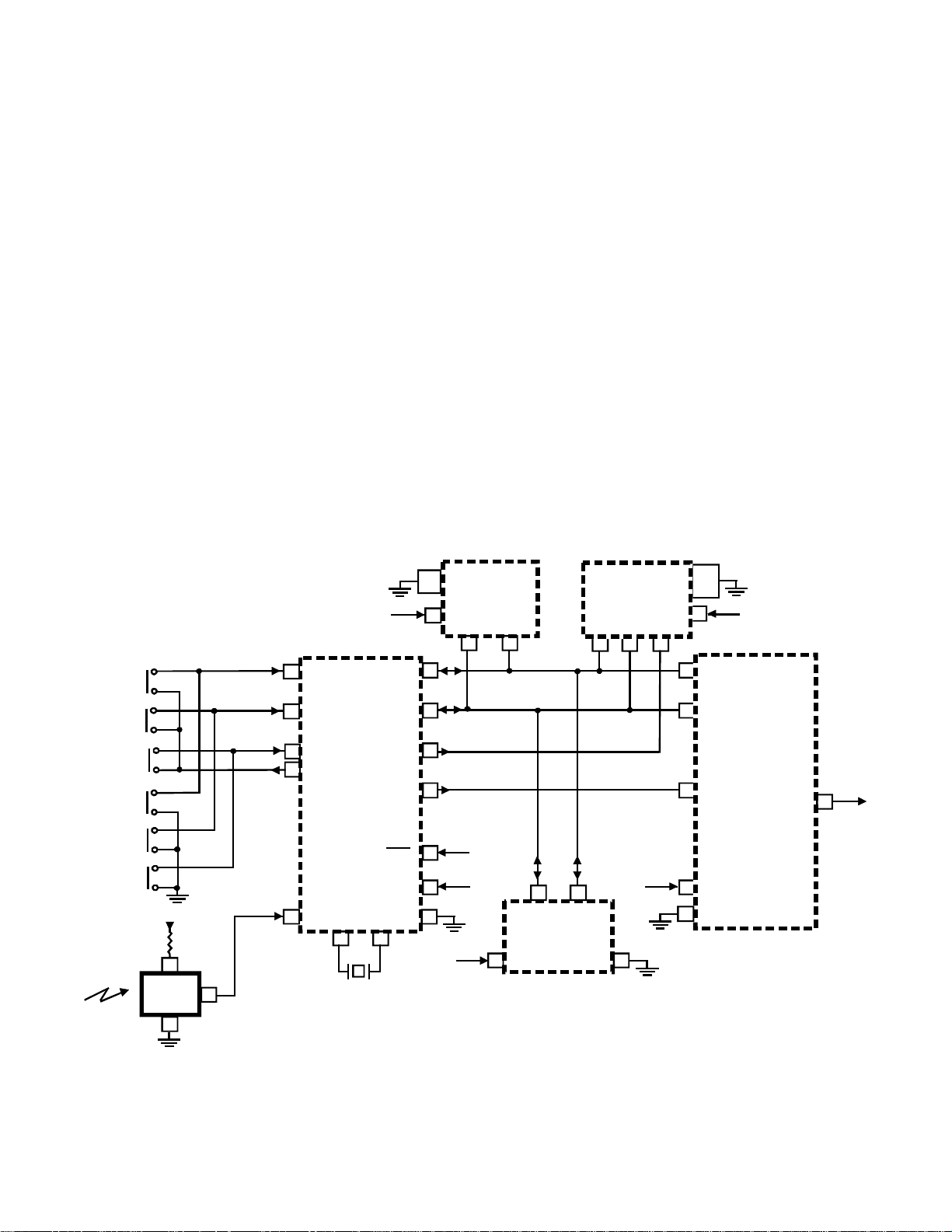
Tech Tips
The following repair information is based on information received from the field. The
symptoms along with their respective solutions are not all inclusive, but will aid in repairing commonly encountered problems.
Dead Set -
Power Supply
Dead Set -
System
Control
POWER
VOL. UP
VOL. DN.
CH. UP
1. R4101 open at U4101 pin 4 (CTC176/77/86/87).
2. Corrupted EEPROM.
3. Immediate U4101 failure caused by an open R4129 or trace open at pin 5, or a
short on the secondary of T4101.
1. Make sure the standby power supplies are working. (12, 7.6 & 5)
2. Check for horizontal drive pulses out of pin 24 of U1001 when the power button is
pressed. If the pulses are there even momentarily, system control is working and the
problem is in the deflection circuits. If the pulses do not appear, check the 7.6 volt
standby voltage on pin 22 of U1001. If the supply is not present on pin 22,
unsolder the pin and see if the supply comes up on the pad. If it does, U1001 is
defective. If it does not, trace the supply back to its source. If 7.6 volts is present
on U1001 pin 22 in circuit, go to the next step.
1,2,3
GND
U3201
4,7
5V
KS1
6
KS2
7
KS3
8
KD1
5
T-CHIP DATA
TUNER CLOCK
T-CHIP CLOCK
TUNER DATA
U3101
µ
P
PIP
ENABLE
T-CHIP
ENABLE
8
15
16
12
14
EEPROM
VDD
DATA CLOCK
5 6
U2901
D-PIP
DATA CLOCK ENABLE
20 21
GND
VDD
22
3,5
15,16
40,41
39 5V
DATA
54
CLOCK
53
ENABLE
52
U1001
T-CHIP
HORZ.
OUT
24
CH. DN.
MENU
5V
2
IR3401
3
5V
1
RESET
7.6 V
5
STBY
GND
13
56
22
BUS
GND
5V
5V
10
4
DATA CLOCK
U7401
TUNER PLL
VCC
VDD
20
OSC
OSC
GND
3
OUT
41 42
1
Y3101
21
IN
Figure 28, CTC175/76/77 System Control Block Diagram
Page 41

Note: ( ) refers to the pins on the Thomson ST-9 microprocessor used on late
production CTC175/76/77 chassis and the CTC186/87 chassis.
3. Check for standby 5 volts on pin 20 (21) of U3101. If it is missing, check the
power supply. If present, go to the next step.
4. Check the reset pin 1 (2) of U3101 for 5 volts. If it is low or missing, check the
reset circuit. If it is, go to the next step.
5. Check pins 41 (36) and 42 (37) of U3101 for a 5 Vpp oscillator. If the signal is not
5 Vpp, check Y3101 and its peripheral components. If the signal is completely
absent, suspect U3101 or Y3101. If the 8 MHz signal is present, go to the next
step.
POWER
VOL. UP
VOL. DN.
CH. UP
CH. DN.
MENU
5V
2
IR3401
3
22
GND
VDD
54
53
52
22
3,5
15,16
40,41
39
DATA
CLOC K
ENABLE
BUS
GND
5V
U1001
T-CHIP
HORZ.
OUT
24
1,2,3
GND
U3201
4,7
EEPROM
5V
KS1
6
KS2
7
KS3
8
KD1
5
1
T-CHIP DATA
TUNER CLOCK
T-C HIP CLOCK
TUN ER DATA
U3101
µ
P
OSC
OUT
PIP
ENABLE
T-CHIP
ENABLE
RESET
VDD
OSC
GND 56
IN
19
20
12
14
21
22
VDD
8
DATA
CLO CK
5
6
5V
2
5V
DATA
20 21
U2901
D-PIP
CLOC K
7.6 V
STBY
ENABLE
36 37
5V
Y3101
TUNER PLL
VCC
10
4
DATA
U7401
5
CLOCK
GND
13
9V
DATA
STEREO DEC ODER
VCC
15
1
CLOC K
U1600
2
3,4,
GND
17
1
CTC186/87 ONLY
Figure 29, System, Control Block Diagram (late production)
Page 42

TECH
TIP
6. Monitor pins 14, 15 (19) and 16 (20) of U3101. There should be no data activity
in the standby mode. When the power button is pressed, 5 Vpp data pulses should
appear. If no pulses appear when the power button is pressed, unsolder pins 20, 21
and 22 of U2901 and pins 4 and 5 of U7401. Now re-check U3101 pins 14, 15
(19) and 16 (20). If data activity returns, suspect a defect in U2901’s or U7401’s
circuit areas. If data activity does not return, go to the next step.
7. Unsolder pins 14, 15 (19) and 16 (20) on U3101 and check for constant 5 Vpp
data pulses in the standby mode on those pins.
Note: When U3101 is initialized, it checks to see if U3201 is present. Under normal
conditions, it immediately finds U3201 and ceases data activity . With the enable,
data and clock lines disconnected, U3101 continues to send out data activity looking
for U3201. This is normal and indicates U3101 is working.
If no data activity is seen on U3101 pins 14, 15 (19) and 16 (20) with the pins out of
circuit, U3101 is probably defective. If data activity is present, reconnect the pins
and go to the next step.
TECH
TIP
8. Having confirmed data activity on pins 14, 15 (19) and 16 (20) of U3101 out of
circuit, disconnect pins 5 and 6 of U3201. Check for data activity in the standby
mode on the circuit board foil side of U3201 pins 5 and 6. If data activity is present
on the foil pads for those pins with the IC out of circuit, U3201 is defective.
Do not throw away the original U3201 until the problem is absolutely confirmed. If
U3201 turns out not to be the problem, putting the old IC back in will prevent a
complete chassis alignment from having to be performed.
If no data activity is seen on the circuit board with U3201 out of circuit, connect the
IC and go to the next step.
9. Unsolder pins 52, 53 and 54 on U1001. Check to see if the data pulses are present
on the foil that leads to the pins. If data pulses are present on the circuit board foil,
U1001 is most likely defective. If no data pulses appear on circuit board foil side of
U1001 pins 52, 53 and 54, suspect an open connection or resistor, or possibly a
leaky capacitor on the data bus.
10. Once the problem is isolated and repaired, do not forget to re-connect U2901,
U7401 and any other parts that may have been unsoldered during troubleshooting.
Audio -
Low/No
Audio -
Buzz
Check the speaker mute logic HI at U3101 pin 29. Replace the EEPROM (U3202)
when HI. The EEPROM data has been corrupted.
Change C4129 from 10µF to 100µF (194366) in the CTC176/77 chassis.
Page 43

Bad connection on the system control and tuner shield tabs.
Front Panel Phantom
Operation
Check for slightly insufficient 5V STBY supply voltage. If low, suspect leaky CR4104
(5.6V zener) in the base circuits of Q4103 and Q4105.
Check for above normal DC voltage and/or noise at U1001 pin 18. Suspect defective
C4501 or C4503.
No On-screen
Display
Vertical
Deflection Non-linear
Page 44
 Loading...