

Page 1

SUPER STEREO
HEADPHONE
AMPLIFIER KIT
Ramsey Electronics Model No. SHA2
Want to listen to your audio source with headphones but the
manufacturer provided no headphone output? No problem;
simply connect the line level output to the input on the SHA2,
connect your stereo headphones, and you’re all set! This is the
next generation headphone amp with the ability to connect
multiple outputs and with more control options than our SHA1.
• Separate volume, treble, bass, balance and loudness
• Signal level clipping indicator LED
• Stereo loop-through for multiple feeds with separate controls
• CD quality audio
• Runs on a 9 volt battery or 12 to 20 VDC external power
SHA2 • 1
Page 2

PARTIAL LIST OF AVAILABLE KITS:
RAMSEY TRANSMITTER KITS
• FM10A, FM25B, FM30, FM Stereo Transmitters
• FM100B, FM35 Professional FM Stereo Transmitters
• AM1, AM25 AM Broadcast Band Transmitters
RAMSEY RECEIVER KITS
• FR1 FM Broadcast Receiver
• AR1 Aircraft Band Receiver
• SR2 Shortwave Receiver
• SC1 Shortwave Converter
RAMSEY HOBBY KITS
• LBC6K Laser Beam Communicator
• SG7 Personal Speed Radar
• SS70C Speech Scrambler/Descrambler
• TT1 Telephone Recorder
• LLS1 Laser Light Show
• MD3 Microwave Motion Detector
• LEDS1 LED Strobe Light
• BE66 Blinky Eyes Animated Display
• LTS1 Laser Trip Sensor
• ICI1C Infrared Switch Control Interface
RAMSEY AMATEUR RADIO KITS
• HR Series HF All Mode Receivers
• DDF1 Doppler Direction Finder Kit
• QRP Series HF CW Transmitters and QAMP Power Amplifiers
• CW7 CW Keyer
RAMSEY MINI-KITS
Many other kits are available for hobby, school, scouts and just plain FUN. New
kits are always under development. Write or call for our free Ramsey catalog.
SHA2 Super Stereo Headphone Amplifier
Ramsey Electronics publication No. SHA2
March 2006
COPYRIGHT ©2005 by Ramsey Electronics, Inc. 590 Fishers Station Drive, Victor, New York
14564. All rights reserved. No portion of this publication may be copied or duplicated without the
written permission of Ramsey Electronics, Inc. Printed in the United States of America.
SHA2 • 2
Page 3

Ramsey Publication No. SHA2:
Manual Price Only $5.00
INSTRUCTION MANUAL FOR
SUPER STEREO
HEADPHONE AMP
TABLE OF CONTENTS
Circuit Description................................ 4
“Learn as you Build”............................. 8
Parts List..............................................9
Parts Layout Diagram........................10
Assembly Steps .................................11
Schematic .......................................... 12
Setup and Testing..............................19
Troubleshooting .................................21
Warranty ............................................23
SHA2 • 3
RAMSEY ELECTRONICS, INC.
590 Fishers Station Drive
Victor, New York 14564
Phone (585) 924-4560
Fax (585) 924-4555
www.ramseykits.com
Page 4

CIRCUIT DESCRIPTION
Let’s take a look at the schematic diagram, we will follow through from input
to output to get a general idea how this kit works, and why. We will look
mainly at the left channel circuitry starting at J1. Items in parentheses ,
‘(xx)’, refer to the right channel signal path. Standard configuration settings
will be assumed. See the optional configurations section for additional
operation information.
The nitty-gritty of it all
A line level audio signal is connected to J1. Line level means an audio signal
of around 1V peak to peak, will give a reading of 0dB on a VU meter. The
audio passes through C9 (C10), a coupling capacitor. This capacitor prevents
DC from entering the circuit from external components and interfering with
audio quality. The capacitor lets the audio pass through to pin 19(2) of U3, an
LM1036, which is the tone/volume/balance control IC.
This IC can be thought of as the heart of the SHA2. It provides control of all
the major functions of the unit including volume, tone, balance and loudness.
Without this IC there would be a large quantity of resistors, capacitors and
amplifiers required to achieve the same functionality it provides. By the way,
remember that it is actually two sets of these controls since this is a stereo
system. R9, R10, R11 and R12 are the volume, tone and balance controls.
These functions are controlled by U3 with a DC voltage applied to the
respective control pins. This voltage is supplied by a built in reference source
on pin 17 and each control varies the voltage on the control pins which is
applied to its control pin. The loudness control, S1A, is used to provide a
slight amount of bass boost when the volume is set to lower settings.
Because your ear is less sensitive to low tones at low levels this provides a
more robust sound at these levels. Capacitors C15 and C21 determine the
way the treble control operates. Capacitors C19, and C20 are for the bass
control while C16 and C18 are used both treble and bass.
After being processed the signal is sent from U3 pin 8(13) to the input of the
output amplifier, U2(U4) pin 3 through C10(C17), another coupling capacitor
like C9. U2(U4) is a fully integrated audio amplifier, capable of driving low
impedance loads. It requires very few external components, runs very
efficiently, and has great fidelity. U2(U4) amplifies the signal to drive a low
impedance speaker like those in your headphones.
R7(R14) and C14(C27) on the output side of the LM386, U2(U4) is for
preventing oscillations due to the inductive nature of a speaker coil being
driven by the LM386. This makes the load of the speaker look more resistive
rather than inductive which prevents “motorboating” of the audio signal.
SHA2 • 4
Page 5

C12(C24) is another coupling capacitor, and it serves the same purpose as
C9 at the start of the circuit. This prevents the DC portion of the signal on the
output of U2(U4) from being sent to the headphones.
The clipping detector circuit
The clipping detector circuit watches the headphone output signal level and
flashes an LED when the output signal comes close to the maximum level
available from the LM386. This level is determined by the voltage divider
formed by R15 and R17.
U1C and U1D form comparator circuits for the left and right channels. The
output signals from U2(U4) pin 5 is fed to U1C(U1D) pin 10(12), the ’+’ or noninverting input, of the comparator. If this signal level exceeds the level on pin
9(13) the output, pin 8(14), will go to a high state about equal to the supply
voltage of 9 volts. This forward biases diode D2(D5), causing it to conduct
and apply a positive voltage through R16 and light the clipping LED D3. R16
is simply a current limiting resistor to prevent D3 from conducting too much
current and ’burning out’. Because the outputs of the two comparators are
basically at ground under non-clipping conditions D2 and D5 are needed so
that if one comparator output goes high and the other is still low the current to
light D3 is not grounded through the low output.
The looping buffer
The purpose of this circuit is to provide a signal which is identical to, but
isolated from, the input signal to feed other devices such as additional SHA2
units, your tape recorder, etc. The isolation feature prevents the additional
devices from interfering with the original input signal. For example if the other
the device were to develop a short it will not affect the unit that it is being fed
from.
U1A(U1B) are used as a unity gain amplifier or buffer. The input signal is feed
through C1(C2), a coupling capacitor, to the buffer amplifier input pin 3(5).
The output of the buffer then goes through C31(C32) to the buffered loop
output. R1(R4) and R2(R3) form a voltage divider which sets a bias level on
the ‘+’ input of the amplifier which is half of the supply voltage. This allows the
input signal to swing around this point and produce an output signal which is
between ground and the power supply voltage. This is basically the same
way the clipping detector works except the output of U1A(U1B) is made to
swing between 0 and the supply voltage as long as the input level does not
exceed a peak-to-peak level greater than the supply voltage. Capacitor C31
(C32) removes the DC level of the output and presents a signal which is
centered around 0 volts to the loop output jack. R19(R18) Provide a path for
C31(C32) to discharge and also sets the impedance of the output. This low
SHA2 • 5
Page 6

impedance makes it possible to connect multiple devices, like the SHA2, with
high impedance to the output without having any significant effect on the
quality of the signal. This is called bridging the output.
Wondering what impedance is? If you know about resistance you know, or I’ll
tell you, resistance is a measurement, in ohms, of the amount of resistance to
current flow in a DC circuit. Like a garden hose that is crimped. There is less
water (current)) flowing in the hose because of the crimp (resistance)).
Impedance is the same thing but is used to describe resistance to an AC
current flow. Why the difference? The resistance (impedance)) of an AC
circuit is affected by the frequency of the AC signal but there is no frequency
involved with a DC signal. The impedance of an amplifier input will be
different for every signal frequency applied to it but a circuit which has only DC
current will always be the same. When an impedance is specified it is usually
for a frequency at the center of the range expected.
What about H1 and H2?
Notice that the input to the looping buffers have a set of jumpers, H1(H2),
feeding them. These jumpers allow you to choose between the direct input
feed to the SHA2 or the output of the LM1036 processor. By connecting a
jumper between pins 1 and 2 of the headers the buffered output is simply
whatever the input is. If the jumper is placed between pins 2 and 3 the
buffered output becomes the processed signal provided to the headphone
amplifiers.
Let’s say that you want to use your SHA2 to listen to the record level output of
your amplifier because it does not have a headphone jack but you also want
to be able to record the program you are listening to. Yes you could simply
connect a ‘Y’ adaptor to the output and plug in the recorder. But what would
happen if the cables to the recorder became shorted to ground. Now you
loose the signal to everything connected to the recorder output. The looping
buffer in the SHA2 will prevent the recorder form affecting your headphones if
the recorder is defective.
Now let’s consider a situation where you have several power amplifiers that
are connected to speakers in different areas. You want to control all the levels
from one central location. By connecting pins 2 and 3 on the headers you can
feed all the amplifiers from the SHA2 and have your monitor headphones too.
How about feeding one signal to a string of monitors for your band. Simply
daisy chain the SHA2’s using the looping buffers. The possibilities are nearly
endless. The choice is yours.
SHA2 • 6
Page 7

The power supply
VR1, C29 and C28 supply the regulated DC voltage for the circuit. VR1
regulates the input, which should be around 12VDC input to J5, to a level of
10VDC for use in the unit. Yes the internal supply voltage indicates it is 9VDC
and here is the reason why. You will notice that diode D1 is connected
between VR1 and the power switch. This diode is to prevent voltage being
applied to the output of VR1 from battery BAT1. Diodes are neat things
because they will only conduct current in one direction such as in this case
when a positive voltage is applied to the anode of the diode with respect to the
cathode. (OK… the cathode is the side of diode to which the arrow points in
the schematic or the end with a band or ‘mark’ on it in the actual device. The
anode is the other side. The cathode likes to be negative with respect to the
anode.) Anyway, you never get something for nothing and in the case of the
diode when it is conducting there is about .6 volts lost across it so the voltage
supplied to the circuitry is around 9.4 volts but we’ll just call it 9VDC.
You will notice that the power jack, J5, has a switch contact which disconnects
the battery from the circuit when external power is being used. This prevents
the battery from attempting to charge when you are using an external power
supply. It is not a good idea to attempt to charge a battery, in fact it can cause
a battery to explode, if the battery is not designed to be charged. NEVER
attempt to charge a standard alkaline or carbon/zinc battery.
SHA2 • 7
Page 8

RAMSEY “LEARN-AS-YOU-BUILD” ASSEMBLY STRATEGY
Be sure to read through all of the steps and check the boxes as you go to be
sure you didn't miss any important steps. Although you may be in a hurry to
see results, before you switch on the power check all wiring and capacitors for
proper orientation. Also check the board for any possible solder shorts
and/or cold solder joints. All of these mistakes could have detrimental effects
on your kit - not to mention your ego!
Kit building tips:
Use a good soldering technique - let your soldering iron tip gently heat the
traces to which you are soldering, heating both wires and pads
simultaneously. Apply the solder to the iron and the pad when the pad is hot
enough to melt the solder. The finished joint should look like a drop of water
on paper - somewhat soaked in.
Mount all electrical parts on the topside of the PC board. This is the side that
has few or no traces on it, the side with the silkscreen writing. When parts are
installed the part is placed flat to the board and the leads are bent on the
backside of the board to prevent the part falling out before soldering (1). The
part is then soldered securely to the board (2-4), and the remaining lead
length is then clipped off (5). Notice how the solder joint looks close up, clean
and smooth with no holes or sharp points (6).
SHA2 • 8
Page 9

SHA2 PARTS LIST
CAPACITORS
5 10 nF ceramic disc capacitors [marked 103] (C3,13,15,21,25)
2 100nF ceramic disc capacitors [marked 104] (C14,27)
2 100pF ceramic disc capacitors (marked 100, 101, or 101K ) (C11,23)
4 220nF ceramic disc capacitors (marked ) (C6,7,8,26)
2 390nF ceramic disc capacitors(C19,20)
14 10uF electrolytic (C1,2,4,9,10,16,17,18,22,28,29,30,31,32)
2 220uF electrolytic (C12, 24)
1 470uF (C33)
RESISTORS
2 2 ohm resistors [red-black-gold] (R7,14)
3 470 ohm resistors [yellow-violet-brown] (R16,18,19)
4 47k ohm resistors [yellow-violet-orange] (R5,6,8,13)
1 100k ohm resistor [brown-black-yellow] (R15)
1 560k ohm resistor [green-blue-yellow] (R17)
4 1M ohm resistors [brown-black-green] (R1,2,3,4)
SEMICONDUCTORS
3 IN4000 series diodes (IN4000 to IN4004) [black body, white band]
(D1,2,5)
1 7810 10V voltage regulator (VR1)
1 Red LED (D3)
2 LM386N low voltage audio power amplifier (U2,4)
1 LM1036N dual DC operated tone/volume/balance IC (U3)
1 LMC660AIN quad rail to rail op amp (U1)
CONTROLS, HARDWARE, AND MISCELLANEOUS
3 100k ohm PC mount potentiometers (R10,11,12)
1 100k ohm PC mount switch potentiometer (R9)
1 9V battery clip (BAT1)
1 9V battery snap
1 DPDT pushbutton switch (S1)
2 3 pin headers (H1,2)
2 Jumper blocks for 3 pin headers
4 3.5mm stereo jacks (J1,2,3,4)
1 2.1mm power jack (J5)
REQUIRED, NOT SUPPLIED
SHA2 • 9
Page 10

SHA2 PARTS LAYOUT DIAGRAM
SHA2 • 10
Page 11

ASSEMBLY STEPS
You’ve got your parts sorted, your iron is warmed up, so let’s get started. We’ll
follow a logical order when installing the parts in your kit. Take your time and
be sure to make good, solid solder connections.
Save a couple of the longer leads that you snip off the back when trimming.
You need one of them for a later step.
Install U3, LM1036N dual DC operated tone/volume/balance IC. You’ll see
the PC board silkscreen shows a notch on one end of the part; this
corresponds to the notch on the IC and shows you which way to place the
part. Line up the notches and make sure that all pins are through the
board. Since no other parts have been installed, when you flip the board
over to solder the part you can have it sit flat on your bench and the board
will hold U3 in place. That way the part will be correctly seated on the
board. That’s why we’re putting the ICs in first! We typically solder the two
corner pins, flip the board over to check placement, then solder the rest.
Install U1, LMC660AIN quad rail to rail op amp. Follow the notched end
for placement and be sure the part is sitting flat on the board before
soldering all the pins.
In the same way, install U2 and U4, the LM386N low voltage audio power
amplifiers. Orient the notched ends and check placement before soldering
all 8 pins on each chip.
Ok, you’re warmed up now. Let’s start installing the smaller components. If
you place the board so that the jacks, J1 through J4 are on the bottom and the
silkscreen writing is facing you so that you can read it, we’ll start at the upper
right corner of the board, near R9. We’ll skip the larger switches, knobs, and
jacks for now and install those at the end.
Install R16, 470 ohm resistor (yellow-violet-brown).
Moving to your left, install R6, 47k ohms (yellow-violet-orange).
Install R5, another 47k ohm resistor (yellow-violet-orange).
Here at the shop we typically insert a number of parts through the
board, bend the leads out so that they stay put, and solder a group of
parts all at one time. Now you don’t want a forest of leads to have to
work through but 5 - 10 part groups seem to work well.
Install C22, the first of many 10uF electrolytic capacitors. These parts
have a polarity and must be installed correctly in order to function. The PC
board silkscreen shows a “+” sign next to one of the holes for the part.
This corresponds to the longer of the two leads, the positive. The negative
SHA2 • 11
Page 12

SHA2 • 12
Page 13

SHA2 • 13
Page 14

lead is not only shorter than the other, it has a band or stripe running
down the body of the part next to the short lead that shows zeros or minus
signs. Be sure to install the part so that the positive lead goes into the
hole marked with a “+” sign and the negative lead into the other. Push the
part down until it sits on the board and solder both leads.
Install C15, 10nF ceramic disc capacitor (marked 103).
Install C6, 220nF ceramic disc capacitor (marked 224).
Install C20, 390nF ceramic disc capacitor (marked 394).
Install C8, 220nF ceramic disc capacitor (marked 224).
Install C16, 10uF electrolytic capacitor. Remember to orient the part
following the “+” sign on the silkscreen and Parts Layout Diagram.
Install R8, 47k ohms (yellow-violet-orange).
Install C3, 10nF ceramic disc capacitor (marked 103).
Install C26, 220nF ceramic disc capacitor (marked 224).
Install C17, 10uF electrolytic capacitor. Remember the polarity when
installing.
Install C7, 220nF ceramic disc capacitor (marked 224).
Install C19, 390nF ceramic disc capacitor (marked 394).
Install C18, 10uF electrolytic capacitor. Watch orientation!
Ok, if you haven’t already done so you might consider a little break at this
point. Rest your eyes, stretch, then take a look at your parts placement and
solder joints to be sure they look great before moving on.
Install C21, 10nF ceramic disc capacitor (marked 103).
Install R13, 47k ohm resistor (yellow-violet-orange).
Install C25, 10nF ceramic disc capacitor (marked 103).
Install C30, 10uF electrolytic capacitor. I’d remind you to be careful how
you install the part, remembering to check the polarity before soldering,
but I don’t want to bug you about it.
Install C13, the last 10nF ceramic disc capacitor (marked 103).
Install C10, 10uF electrolytic capacitor. Polarity.
Install C11, 100pF ceramic disc capacitor (marked 100, 100K, or 101).
SHA2 • 14
Page 15

Install C14, 100nF ceramic disc capacitor (marked 104).
Install R7, a 2 ohm resistor (red-black-gold).
Install C23, 100pF ceramic disc capacitor (marked 100, 100K, or 101). It’s
tucked in between U2 and U4.
Install C27, 100nF ceramic disc capacitor (marked 104).
Install R14, 2 ohms (red-black-gold).
Install C12 and C24, both 220uF electrolytic capacitors. These are slightly
larger than the 10uF caps you’ve been installing but the same rules apply
as to polarity. Follow the stripe or band for the negative lead and place the
longer positive lead in the hole marked with a “+” sign.
Now we’ll move back up and toward the middle of the board. Hopefully you’re
not having too much trouble seeing where the parts are supposed to be
placed.
Install C4, 10uF electrolytic capacitor. Please orient it properly. Thanks!
Install D5, 1N4000 series diode, another polarity sensitive component.
The white band on the part and the white band shown on the silkscreen
need to line up with each other. Solder as usual.
Install R17, 560k ohms (green-blue-yellow).
Install R15, a 100k ohm resistor (brown-black-yellow).
Install C33, 470uF electrolytic capacitor. Remember the rules for
electrolytic caps and follow the “+” sign.
Install D1, 1N4000 series diode. The white band shows the way to place
the part.
While you’re clipping leads on the back side of the board you can also
check the solder joints and immediately touch up any that don’t look
right. You’re already looking at the connections closely and it’s a good
time to spot mistakes!
Install VR1, the 7810 10V voltage regulator. The writing on the part should
face the outside of the PC board. Bend the center lead out so that the part
fits into the holes and solder it in.
Install D2, 1N4000 series diode. Again, follow the white band on the board
and on the part for orientation.
Install R3, 1 M ohm resistor (that’s a million ohms!) (brown-black-green).
SHA2 • 15
Page 16

Install R4, another 1 M ohm resistor (brown-black-green).
Install C28, 10uF electrolytic capacitor. Remember the polarity yet again.
Install C29, 10uF electrolytic capacitor. Placement.
Install C9, 10uF electrolytic capacitor. Watch your placement..
Install C2, yup, another pesky 10uF electrolytic. The lead with the band
goes in the hole opposite the one marked with the “+” sign, as usual.
Install R1 and R2, both 1 M ohm resistors (brown-black-green).
Install H2, one of the three pin headers. The long pins stick up from the
board and the short pins go into the board to be soldered.
Install C32, yet another 10uF electrolytic capacitor.
Install R19, 470 ohm resistor (yellow-violet-brown). You’ll find it between
J1 and J2.
Install H1, the other three pin header.
We’re in the home stretch now, just a few more parts to install. Take a break
when you need to and then let’s get building again.
Install C1, 10uF electrolytic capacitor. Positive lead, “+” hole.
Install C31, 10uF electrolytic capacitor, and this is the last time you’ll have
to hear about polarity and orientation. Refreshing, isn’t it?
Install R18, 470 ohms (yellow-violet-brown), between J2 and J3.
Jacks, pots, switches and we’re just about ready to fire up your headphone
amp.
Starting at the left and working our way to the right, let’s install J4, one of
the 3.5mm stereo jacks. This part and the rest of the jacks and switches
will want to sit flatly and nicely on the PC board so that the kit fits well
when you go to case it up and so that you don’t have trouble plugging
things in, etc. Take your time and do it right, and we’re almost finished
anyway so a few extra minutes here won’t cost you much but will pay off
in the end.
In the same way, install J3, another 3.5mm stereo jack. Remember when
headphone jacks were all 1/4”? Now they’ve all gone over to 3.5mm. Of
course some of us remember those single ear, cream colored earphones
you’d get with your transistor radio. Hmmm, kind of dating myself now,
huh? Ok, let’s get back to building!
Locate the DPDT switch and install it in the S1 position. Happily, I have no
SHA2 • 16
Page 17
stories about DPDT switches to bore you with.
Back to jacks, install J2 and while you’re at it, let’s install J1 and get it over
with. Both are 3.5mm stereo jacks.
Now install J5, the 2.1mm power jack.
Time to install the 9V battery holder. This is where you’ll need that clipped
off lead from the beginning of your construction. This is bent into the
shape of a staple that will fit through the holes in the battery holder and
down through the top of the circuit board. Once the holder is on the board
with the “staple” through it, bend the leads out on the backside of the
board to hold them in place, then solder. The tighter the bend the less
slop you’ll have in the battery holder. If you want it perfectly tight then get
it where you want it and solder the “staple” wire right to the battery clip on
the topside of the board.
We still have to flip the board over a few more times so let’s install the battery
snap last; that way it won’t flop around too much.
Install R9, the 100k ohm PC mount switch potentiometer. It’s different
from the other three and easy to spot.
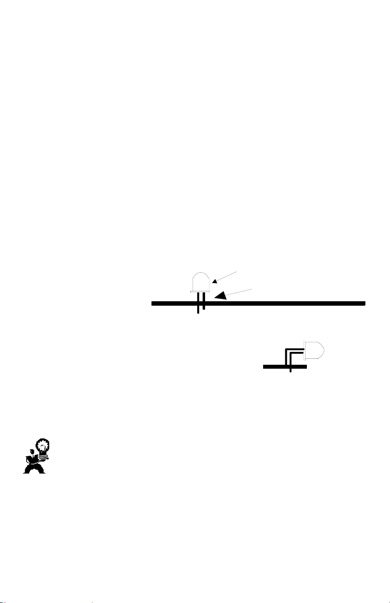
Before we
install R10
we’d better
install D3, the
mini red LED.
LED
longer lead = positive
+
-
shorter lead, flat side = negative lead
Leave these leads
as short as possible
PC Board
The part has a flat side and a flat edge is shown
on the PC board for orientation. This part will be
Side view
bent over and the LED will be sitting on the board
when you’re finished. In other words, very short
lead length above the board.
front of PC board
Install R10, R11, and R12, 100k ohm PC mount potentiometers. These
parts will want to sit flat on the board before you solder them. They like it
that way.
I like to solder the 3 center leads on the pots, then take my time and
solder all the ground connections on each one. The ground connections
will take a bit more time because the surface area of the ground plane
is larger than the small pads you’re used to. But don’t worry, you won’t
hurt anything leaving the iron on a bit longer with these connections. In fact,
you'll have to do it that way to get a solid solder joint. And soldering all the
grounds together will actually make it easier since the plane will stay hotter as
you keep working from one connection to another.
SHA2 • 17
Page 18

The battery snap is the last part to be installed. The red lead goes into the
hole marked with a “+” sign and the black goes into the “-” hole. You can
tin the leads by twisting them together and melting some solder on them
or you can simply twist them, put them through the board, and solder
them. It’s up to you. Just don’t tin them so much that they don’t fit through
the holes in the board.
That’s it! But wait, before you grab a battery and fire up your kit let’s check a
few things. Mainly check the orientation of the ICs, diodes, and all those
electrolytics. We don’t want anything to go “pop” when we apply power, right?
Also check your solder joints for any that are less than perfect and make sure
that all the solder connections you see on the back are supposed to be there.
Bridges can be dangerous to your circuit. Be sure none of your clipped off
wires have lodged between the connections on the back. When you’re
satisfied we’ll move on and give your headphone amp a try.
SHA2 • 18
Page 19

SETUP AND TESTING
It’s time to apply power to your SHA2 and start listening to your line level
sources.
You need:
• An AC adapter or a fresh 9 volt battery
• A line level audio source (CD player line out, etc.)
• A cable to connect the audio source to the SHA2. Either dual RCA to
3.5mm stereo or 3.5mm stereo to 3.5mm stereo, depending on what
connector(s) are on your line level source.
• Headphones
1. Connect your audio source to J1, the line level audio input jack.
2. Connect your headphones to either J3 or J4, the headphone outputs.
3. Connect your DC supply or 9 volt battery.
4. Turn on your line level source.
5. Turn on your SHA2. The LED, D3, should light and then go out after a few
seconds. Turn the volume up to a comfortable level.
6. You should be hearing your line level audio source at this point. Now try
the balance control, R12, and get the balance between left and right set
where you want it.
7. Try out the treble control, R10, and the bass control, R11, and set them
for the sound you want.
8. Next try pressing in S1, the loudness control. You should hear the
difference immediately. It almost sounds like a bass boost but you’ll notice
that the overall loudness increases too.
9. Plug another set of headphones into the other headphone jack and try
that out too.
When you first see your LED light you may think that it’s a power on indicator,
and it is temporarily when you first turn on the kit. After that it’s a clipping
indicator, showing you when the audio level is close to the maximum output of
the IC. During typical operation this LED will be off.
The buffered loop output, J2, allows you to connect the line level audio output
of your SHA2 to another device. You can set the SHA2 up so that the output
is directly coupled, just as if you had your line level source connected right to
the other device, or you can send the line level audio to another source with
the tone controls added. This is done using jumper headers H1 and H2.
SHA2 • 19
Page 20

You can set the left and right channels independently of each other. H1
controls the right channel of the stereo output and H2 controls the left channel.
Pin 1 on both H1 and H2 is marked by a triangle. By placing a jumper block
between pins 1 and 2 of H1 and H2, the buffered output follows the input
exactly. Whatever you have coming in on the audio input is what will be sent
out on J2. Placing the jumper block between pins 2 and 3 of H1 and H2
causes the buffered output to have the same tone controls applied to it as the
headphone output. You can put the jumper block on H1 and not H2, on H2
and not H1, etc. so that one channel would have tone control applied to it and
the other would exactly follow the input. It’s all up to you.
Once you have the jumpers set, try plugging the buffered output into the line
level input on a piece of equipment and make sure it’s working correctly. If you
have the tone controls set and have H1 and H2 jumpered for it you should be
able to hear that the original line level source has been changed and now
matches what you’re hearing through the headphones.
That’s about it. You’re ready to start using your SHA2.
One last thought about the buffered output. You can use it to daisy chain more
than one SHA2 so that all headphone outputs on the chain are hearing the
same source. Simply plug the buffered output of the first SHA2 into the line
level input of the second SHA2. Now you have 4 headphone jacks all on the
same “channel”, all hearing the same audio. Think of the possibilities for long
car trips. A portable DVD player with a line level audio output, 2 to 4 children
in the back of a minivan all happily listening to a movie on their own
headphones, peace and quiet for the driver. Sounds lovely, doesn’t it?
We’re sure you’ll come up with other uses for your SHA2, such as plugging
the line level output of your Bose radio into it so that you can listen on
headphones. Or plugging a line level audio source into your Ramsey FM
transmitter through an SHA2 so that you can monitor the broadcast without
having to tune in an FM radio. And there are probably many other applications
that we haven’t even thought of yet. Let us know if you come up with
something interesting, ok?
SHA2 • 20
Page 21

TROUBLESHOOTING
While we hoped it wouldn’t come to this, it’s possible that your SHA2 didn’t
work as soon as you applied power. The main thing to remember in a situation
like this is . . . don’t panic! It’s usually something simple and since you built
the kit, you know the kit and you’ll find it if you look carefully. Just follow a
logical approach when troubleshooting.
The first thing to check is always your component placement, especially ICs,
diodes, and electrolytic capacitors. Make sure that the resistors with similar
color bands haven’t been switched. Then flip the board over and make sure
that all the solder connections look good, that none have been missed, and
that there are no bridged connections that don’t belong. 90% of the problems
we see on kits that have been sent in for repair are construction errors of one
kind or another so this really is the place to start.
Check your headphones on a different source to be sure they aren’t the
problem. This is also a good thing to do if the SHA2 seems noisy because it’s
probably not the kit but may well be a poor connection inside the headphones.
The next step may seem obvious but we’ll state it anyway. Be sure you have a
good 9 volt battery or a good power source if you’re using a wall transformer.
A multimeter is helpful here. Also be sure that the tip of the adapter is positive,
especially if you didn’t get it from Ramsey. A meter isn’t the best way to test a
battery but it will tell you if a 9 volt is beyond hope. A battery tester will put the
battery or cell under a load and give you a better indication of its condition. If
the input power from your regulated supply or wall transformer is good you
can check your regulator to see what’s coming in and if you have a good 10
volts going out. (This does not apply if you’re using a 9 volt battery; the kit
runs directly from the battery and bypasses the regulator.) If the output of the
regulator is good then you can take a look at the schematic and note the
power input pins on the ICs, then check them to be sure they’re being
supplied with the correct voltages.
Beyond these checks you’ll need some test equipment such as an
oscilloscope to follow your line level source through until you see the signal
stop. You can read the warranty instructions on the inside back cover of this
manual and send the kit in for repair If you get in over your head. All the
information for returning a kit to Ramsey for repair is on that page.
If you need help you can call Tech Support at 585-924-4560 and speak with a
technician. You can expect to be taken back over the ground covered above
when you call, so be prepared. We can tell the people who read through the
troubleshooting and checked their kit over from the ones who panicked and
called before checking. But rest assured that one way or another you’ll have a
working SHA2 when all is said and done.
SHA2 • 21
Page 22

If you enjoyed this Ramsey product, there are plenty more to choose from in
our catalog - write or call today!
CONCLUSION
We sincerely hope that you will enjoy the use of this Ramsey product. As always, we have tried to compose our manual in the easiest, most “user
friendly” format possible. As our customers, we value your opinions, comments, and additions that you would like to see in future publications. Please
submit comments or ideas to:
Ramsey Electronics Inc.
Attn. Hobby Kit Department
590 Fishers Station Drive
Victor, NY 14564
or email us at: techsupport@ramseymail.com
And once again, thanks from the folks at Ramsey!
SHA2 • 22
Page 23

The Ramsey Kit Warranty
Please read carefully BEFORE calling or writing in about your kit. Most
problems can be solved without contacting the factory.
Notice that this is not a "fine print" warranty. We want you to understand your rights and ours too! All
Ramsey kits will work if assembled properly. The very fact that your kit includes this new manual is your
assurance that a team of knowledgeable people have field-tested several "copies" of this kit straight
from the Ramsey Inventory. If you need help, please read through your manual carefully, all information
required to properly build and test your kit is contained within the pages! However, customer
satisfaction is our goal, so in the event that you do have a problem, take note of the following.
1. DEFECTIVE PARTS: It's always easy to blame a part for a problem in your kit, Before you conclude
that a part may be bad, thoroughly check your work. Today's semiconductors and passive components
have reached incredibly high reliability levels, and its sad to say that our human construction skills have
not! But on rare occasions a sour component can slip through. All our kit parts carry the Ramsey
Electronics Warranty that they are free from defects for a full ninety (90) days from the date of
purchase. Defective parts will be replaced promptly at our expense. If you suspect any part to be
defective, please mail it to our factory for testing and replacement. Please send only the defective part
(s), not the entire kit. The part(s) MUST be returned to us in suitable condition for testing. Please be
aware that testing can usually determine if the part was truly defective or damaged by assembly or
usage. Don't be afraid of telling us that you 'blew-it', we're all human and in most cases, replacement
parts are very reasonably priced.
2. MISSING PARTS: Before assuming a part value is incorrect, check the parts listing carefully to see if
it is a critical value such as a specific coil or IC, or whether a RANGE of values is suitable (such as
"100 to 500 uF"). Often times, common sense will solve a mysterious missing part problem. If you're
missing five 10K ohm resistors and received five extra 1K resistors, you can pretty much be assured
that the '1K ohm' resistors are actually the 'missing' 10 K parts ("Hum-m-m, I guess the 'red' band really
does look orange!") Ramsey Electronics project kits are packed with pride in the USA. If you believe
we packed an incorrect part or omitted a part clearly indicated in your assembly manual as supplied
with the basic kit by Ramsey, please write or call us with information on the part you need and proof of
kit purchase.
3. FACTORY REPAIR OF ASSEMBLED KITS:
To qualify for Ramsey Electronics factory repair, kits MUST:
1. NOT be assembled with acid core solder or flux.
2. NOT be modified in any manner.
3. BE returned in fully-assembled form, not partially assembled.
4. BE accompanied by the proper repair fee. No repair will be undertaken until we have received the
MINIMUM repair fee (1/2 hour labor) of $25.00, or authorization to charge it to your credit card account.
5. INCLUDE a description of the problem and legible return address. DO NOT send a separate letter;
include all correspondence with the unit. Please do not include your own hardware such as nonRamsey cabinets, knobs, cables, external battery packs and the like. Ramsey Electronics, Inc.,
reserves the right to refuse repair on ANY item in which we find excessive problems or damage due to
construction methods. To assist customers in such situations, Ramsey Electronics, Inc., reserves the
right to solve their needs on a case-by-case basis.
The repair is $50.00 per hour, regardless of the cost of the kit. Please understand that our technicians
are not volunteers and that set-up, testing, diagnosis, repair and repacking and paperwork can take
nearly an hour of paid employee time on even a simple kit. Of course, if we find that a part was
defective in manufacture, there will be no charge to repair your kit (But please realize that our
technicians know the difference between a defective part and parts burned out or damaged through
improper use or assembly).
4. REFUNDS: You are given ten (10) days to examine our products. If you are not satisfied, you may
return your unassembled kit with all the parts and instructions and proof of purchase to the factory for a
full refund. The return package should be packed securely. Insurance is recommended. Please do not
cause needless delays, read all information carefully.
SHA2 • 23
Page 24

TABLE OF CONTENTS
Circuit Description................................4
“Learn as you Build”............................. 8
Parts List ..............................................9
Parts Layout Diagram ........................10
Assembly Steps .................................11
Schematic .......................................... 12
Setup and Testing..............................19
Troubleshooting .................................21
Warranty ............................................23
REQUIRED TOOLS
• Soldering Iron (WLC100)
• Thin Rosin Core Solder (RTS12)
• Needle Nose Pliers (MPP4 or RTS05)
• Small Diagonal Cutters (RTS04)
ADDITIONAL SUGGESTED ITEMS
• Helping Hands Holder for PC Board/Parts
(HH3)
• Technician’s Tool Kit (TK405)
• Desoldering Braid (RTS08)
• Digital Multimeter Ramsey M133
RAMSEY ELECTRONICS, INC.
590 Fishers Station Drive
Victor, New York 14564
Phone (585) 924-4560
Fax (585) 924-4555
www.ramseykits.com
SHA2 • 24
Assembly and Instruction manual for:
Super Stereo Headphone Amplifier
TOTAL SOLDER POINTS
214
ESTIMATED ASSEMBLY
TIME
Beginner............... 3 hrs
Intermediate......... 1.5 hrs
Advanced............. 1 hr
Manual Price Only: $5.00
Ramsey Publication No. SHA2
RAMSEY MODEL NO. SHA2
 Loading...