

RAM 1500, 2000, 3000, 6000, 3004 Service Manual
...
SERVICE MANUAL
P-5343-006
QXPSDoc
1/07
© 2007 by C.E. Studio-2 s.l. - Spain (EEC)
http://www.ramaudio.com
e-mail: support@ramaudio.com
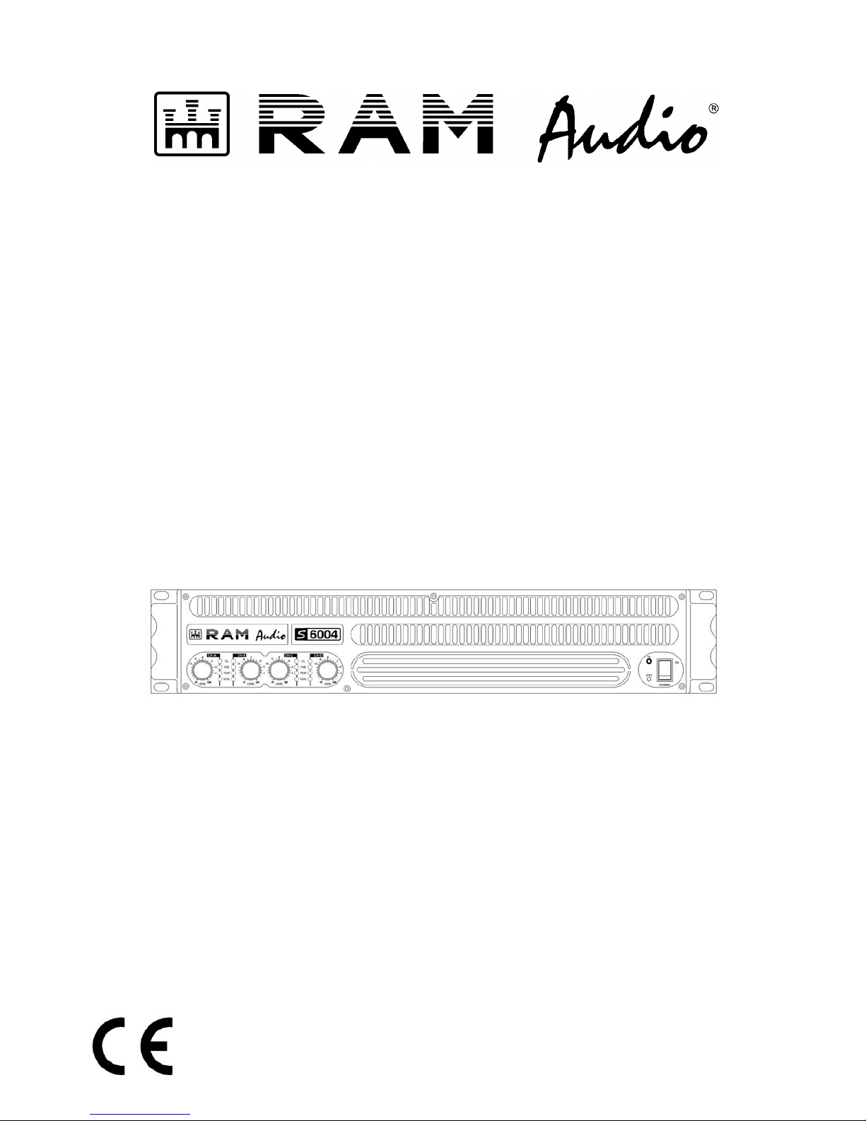
Professional Power Amplifiers
S Series
1500-2000-3000-4000-6000
3004-4004-4044-6004-6044
WARNING:
The exclamation point inside an equilateral triangle indicates
the existence of internal components whose substitution may
affect safety.
The lightning and arrowhead symbol warns about the presence of uninsulated dangerous voltage.
To avoid fire or electrocution risk do not expose the unit to rain or moisture.
To avoid electric shock, do not open the unit. No user serviciable parts inside.
In the case of disfunction, have the unit checked by qualified agents.
SAFETY PRECAUTIONS
CAUTION
RISK OF ELECTRIC SHOCK
DO NOT OPEN
©2010 by C.E. Studio-2 s.l.
Pol.Ind. La Figuera
C/ Rosa de Luxemburgo, 34
46970 Alaquas - Valencia - SPAIN
Phone: +34 96 127 30 54
Fax: +34 96 127 30 56
http://www.ramaudio.com
e-mail: support@ramaudio.com
RAM Audio
®
, PMS™, SSP™, ICL™and QuantaPulse™is registered trademarks of C.E. Studio-2 s.l.. All
other names are trademarks of their respective companies.

The S series is a hi power amplifier composed by 2 or 4 channel class H technology fed by a switching power
supply. It has twin male-female XLR back pannel input connectors per channel with the posibility to work in stereo, parallel or bridge modes. Has too a gain selection switch which permits work at 26, 32 or 38 dB, and a
selectable subsonic filter. It has four front pannel indicators per channel to inform the amplifier operative status
and a potentiometer attenuator per channel to adjust the output level.
At the back pannel there are the output Speakon audio connectors. It has too a three wire power mains cord
to connect the amplifier to a properly voltage and current rated mains network with earth connection.
Audio circuit description
The circuit input has a balanced (differential) amplifier to reject the common mode noise added to the audio
signal. Then the signal passes through the gain amplifier, subsonic filter and the clip limiter gain control that is
innactive unless the amplifier will be in clipping situation due to excesive input signal.
Following this, the signal arrives to the properly named power amplifier. This circuit is comprised by an opamp
that provides the error signal to a class A voltage amplifier that feeds the common emitter power amplifier. The
feedback signal from the output is returned to the opamp that performs the corrections necessary to replicate at
the output the amplified input signal.
Inside the class A voltage amplifier is inserted a bias control circuit that provides a operating point to the following power stage and compensates the thermal derating of silicon PN junctions avoiding the thermal runaway
problem.
Inside the power stage is implemented a current limiting circuit that avoid to excessive power transistors disipation in case of shortcircuit or very low impedance loads. The actuation of this circuit limits the output to secure
levels.
Following the power amplifier circuit there are a zoobel network and a coil in series that provides correct
amplifier performing and inconditional stability in case of excesive inductive or capacitive loads.
The power supply simetrical rails come from the class H conmutation matrix. This matrix is composed by
mosfet transistors and diodes and selects the most suitable voltage level to feed the amplifier depending of the
output signal level. This operating method leads to a very low power disipation in the power transistors. The mosfets in the conmutation matrix are commanded by a voltage comparator which output depends of the output signal and the supply rails voltage.
There is an on board fan control to regulate the fan speed depending of temperature that is sensed via a ntc
thermistor attached to the heatsink.
Regarding to the protection systems there are several blocks which comprise:
- DC protection, via a low pass filter that detects DC or very low frequency signal at the output.
- Shortcircuit protection.
- High temperature protection, via the ntc thermistor and a comparator with a fixed absolute reference.
- Power on delay, via a timer that sets the time between power on and full operative status.
- Clip limiter
Regarding the front pannel indicators, all of them are commanded from the audio power section, providing
visual information for fault, ok status, high temperature, clipping and input signal existence.
GENERAL DESCRIPTION

GENERAL DESCRIPTION
Power supply description
The amplifier has a switching power supply fully independent and self commanded and protected, to feed the
DC voltage to the audio power section.
The mains voltage passes through an interference filter to filter out both the switching noise to go out and the
mains interference to come in. Then is located the main fuse and power on switch that when closed permits the
charging of primary capacitors via the soft start circuit and the diode bridge. After a few seconds the soft start circuit is bypassed and full mains voltage is applied to the primary side. From the capacitors DC voltage an inverter
implemented by two power transistors creates a high frequency square wave that feeds the high frequency transformer primary winding. From the multiple secondary windings several dc voltages are built via the corresponding rectifiers, inductances and capacitors too feed the audio power section.
The control of the entire power supply is done from a separate board with contains all the necessary circuitry.
This circuitry is fed via its own power supply, fully independent, located in the same board. Inside the board are
located the power transistor drivers and clock generator for the high frequency signal. Beside, are located too the
soft start control and the power supply protections, that are:
- Power off or mains voltage absence detector
- Low/high mains voltage detector
- Excessive peak or average primary current detector via a current sensor.
- DC output shutdown
All these protections act stopping the high frequency oscillation and restarting the system configuring a very
fast acting way to protect the power supply. The current detector circuit try first to lower the amplifier gain to
reduce the current consumption, stopping the oscillation as a seconday action. Also, the audio section can send
information to the power supply to stop the oscillation, if you have DC output.

TECHNICAL SPECIFICATIONS
Technical Specifications
S-1500 S-2000 S-3000 S-4000 S-6000 S-3004 S-4004 S-4044 S-6004 S-6044
Output Power
1kHz, 1.0% THD+N
@ 2Ω 2x 880 W 2x 1190 W 2x 1570 W 2x 1950 W 2x 2950 W 4x 700 W 4x 980 W - 4x 1440 W -
@ 4Ω 2x 575 W 2x 790 W 2x 1100 W 2x 1380 W 2x 2025 W 4x 500 W 4x 670 W 4x 975 W 4x 1000 W 4x 1480 W
@ 8Ω 2x 325 W 2x 460 W 2x630 W 2x 810 W 2x 1250 W 4x 300 W 4x 430 W 4x 690 W 4x 620 W 4x 10¹⁵ W
Bridge @ 4Ω 1760 W 2380 W 3140 W 3900 W 5900 W 2x 1400 W 2x 1960 W - 2x 2880 W -
Bridge @ 8Ω 1150 W 1580 W 2200 W 2760 W 4050 W 2x 1000 W 2x 1340 W 2x 1950 W 2x 2000 W 2x 2960 W
Pink Noise 12dB C.F.
@ 2Ω 2x 975 W 2x 1360 W 2x 2060 W 2x 2460 W 2x 4225 W 4x 890 W 4x 1170 W - 4x 2080 W -
@ 4Ω 2x 610 W 2x 880 W 2x 1240 W 2x 1600 W 2x 2600 W 4x 580 W 4x 820 W 4x 1230 W 4x 1280 W 4x 2110 W
Frequency Response
Power Bandwidth ±0.25dB 20Hz-20kHz
Phase Response
@ 1 watt 20Hz-20kHz ±15 deg
Total Harmonic Distortion
20Hz-20kHz <0.05%
Intermodulation Distortion
SMPTE <0.05%
Damping Factor
20-500Hz @8Ω >500
Crosstalk
20Hz-20kHz >75 dB
Voltage Gain 26/32/38 dB
Sensitivity
Rated Power @ 8Ω (V) 2.6/1.3/0.6 3.0/1.5/0.8 3.6/1.8/0.9 4.0/2.0/1.0 5.0/2.5/1.3 2.6/1.3/0.6 3.0/1.5/0.8 3.7/1.9/0.9 3.5/1.8/0.9 5.0/2.5/1.3
Signal-to-Noise Ratio
20Hz-20kHz 112 dB 113 dB 115 dB 116 dB 118dB 112dB 113dB 116dB 116dB 118dB
Required AC Mains
230 V - 50 Hz (idle) 0.5 A 0.5 A 0.5 A 0.5 A 0.5 A 0.5 A 0.5 A 0.5 A 0.5 A 0.5 A
@ 4Ω (1/8 rated power) 4 A 4.8 A 6.2 A 7.5 A 10.5A 6 A 7.5 A 11A 10.5A 15A
Dimensions
W x H x D (mm) 483x89x310
W x H x D (inches) 19x3.5x12.2
Weight
Net (Kg- Lbs) 8-17.6 8-17.6 8.5-18.7 8.5-18.7 8.6-18.9 8.5-18.7 8.5-18.7 8.5-18.7 8.6-18.9 8.6-18.9
Protections
Soft-start, Turn-on Turn-off transients, Muting at turn-on, Over-heating, DC, RF, Short-circuit, Open or mismatched loads, Overloaded
power supply, ICL
™
, PMS™, SSP
™

QUICK REPAIR PROCEDURE
MAINS CURRENT LIMITER:
To test the power amplifier it is advisable to implement a mains current limiter to avoid any shortcircuit, in
case the unit has damaged parts that have not been fixed. The most effective and easy solution is to use a pair
of 100W light bulbs arranged in parallel, and placed in series with the mains supply. If everything is OK, when
you switch on the power supply the bulbs will light until the primary capacitors are fully charged and then they
will bright softly enabling enough current to pass through to reach a normal start up of the supply.
POWER SUPPLY:
When the switching power supply breaks, the usual consequences are that both IGBT transistors (Q2 & Q3)
explode and that the IR2110S ic (U12) from the control board (the IGBT driver) gets damaged. It may be possible that more ic's from the control board get damaged too (U15 SG3525 or U9 NE555), but this is not usual.
Once an IGBT breaks, it is absolutely necessary to change the IR2110S ic too, even if it seems to be OK. If the
IR2110S ic is not replaced, the IGBTs will damage again. If you have not the requiered SMT tools to change any
SMD component, the best option is to change the complete control board.
To change the IGBTs follow the next steps: take out the power supply unit from the amplifier by removing the
screws at the PCB. Put the power supply PCB upside down and unscrew the 4 screws that are on the IGBT
heatsink, remove both switching transistors by cutting their legs and clean the pad holes of solder. Screw another
pair of transistors to the heatsink with their corresponding mica insulators, and place the heatsink again into its
location by fastening the other two screws and soldering the transistors legs to the PCB. Above manipulations
must be done with utmost care in order to have a successful repair. Check that the transistor collector is insulated from the heatsink and that this heatsink is located parallel to the other one. Change the control PCB and do a
visual test of the rest of the components.
Test too the integrity of secondary rectifiers using a multimeter in "diode mode". Test also they are insulated
from the heatsink. (D9, D10, D11, D12, D13, D14, D15 and D16).
To test the power supply it is advisable to implement a little bench to avoid any risk because of lack of insulation from direct ac mains voltage in most of the circuit. We recommend to use a transformer with turns ratio 1:1
to isolate the mains from the power supply (remember that the 230 V ac is still present) but now you are isolated
from earth. Connect the power supply through the current limiter (bulbs in series with the mains) and you must
look at the control board green led to check that the 15Vdc control board supply is operating and that there is not
any shorted ic. You can measure then the voltages at the output connector, they will be lower than expected
because the voltage drops at the bulbs. The voltages are the following:
S 1500: ±49V / ±81V
S 2000: ±49V / ±98V
S 3000: ±65V / ±114V
S 4000: ±65V / ±130V
S 6000: ±54V / ±108V / ±162V
S 3004: ±49V / ±81V
S 4004: ±49V / ±98V
S 4044: ±65V / ±130V
S 6004: ±38V / ±76V / ±115V
S 6044: ±54V / ±108V / ±162V
When you are sure that the unit is OK, you can short the light bulbs with the aid of a switch and measure the
correct voltages.
Bear in mind that it is possible that one of the audio power section may be damaged. Test there is no short at
the power transistors. Verify also there is not any ground track opened. When switching the amplifier on, measure that the voltage at the power audio section emitter resistors correspond to the first class H level. Check with
an oscilloscope, with the probe attached to the emitter resistors, that when applying signal the power supply will
change in steps as expected. Test both polarities.
It is highly recommended to test the entire amplifier with the light bulbs in series with the mains supply to
avoid further power supply breakings. If the amplifier start up correctly then you may short the light bulbs and
apply signal to obtain power from the amp.

QUICK REPAIR PROCEDURE
POWER AUDIO SECTION:
When the audio section breaks, the usual consequences are that some final transistor or/and driver transistor
gets shortcircuited. It is possible to get also some class h conmutation mosfet transistor or diode shortcircuited.
To check it you have to use a multimeter in diode mode or resistance measure. If the final transistors are OK you
can measure around 10ohms between the base and the emitter and very high resistance between collector and
emitter. In the driver transistor you have to measure around 230ohms between base and emitter.
If you have a final transistor shortcircuited, you can measure a very low resistance between collector and
emitter of all final transistors, but the lower resistance indicates what is exactly the transistor shortcircuited,
because this has a direct shortcircuit and the other paralleled transistors have arround 0.66ohms (two serie
emittter resistor). Cut the leads of this shortcircuited transistors and continue testing if you have some more transistor broken.
Also, you may have only the driver transistor shorcircuited, then you can measure this direct shorcircuit between collector and emitter of this transistor, and arround 10ohms betweem the collector and emiter of the all final
transistors. Also it is possible to have the driver and some final transistor broken. Cut the leads of any device
broken and continue testing until you are sure you have not any more device shorcircuited.
You have to check also the mosfet transistor and diode from the class H switch. They are placed on the same
heatsink nearest to the fan. Check you have not a shortcircuit between the drain and the source of the mosfet
and check the diode works correctly.
To change any device broken you have remove the heat sinks needed to reach it. Now remove his screw and
place the new one with thermal silicone. Clean the surface if needed. Tight the screew using a screewdriver with
a torque arroud 1.3N/m.
Its is possible you have to change some burn resistor. Check visually specially the 0.33ohms emitter resistor
and the 10ohms/1W driver emitter resistor, and if you have some dark resistor measure it and change if needed.
After change all broken devices, check you have not any shorcircuit between the outputs (heat sink), rails and
ground. It is highly recommended to test the entire amplifier with the light bulbs in series with the mains supply to
avoid further power module breakings. If the amplifier start up correctly then you may short the light bulbs and
apply signal to obtain power from the amp. Use 1kHz sinusoidal signal and 4 ohms dummy load to test all works
perfectly. Check specially the switch rail works correctly, and you have not any instability when you clip the output.
If the signal input clips before as expected, perhaps you can have some problem with the SOA limit circuit.
Some small SMD transistor can be broken. Check if you have problems with the positive or negative semicycle
and test the SOA limit components, placed in front of the heat sink. This circuit controls the maximun transistor
current and you can test it working with a very low impedance load (1ohm for example) and a small input signal.
you can see this system limits the output to a secure value.
Bias adjusting: you may adjust the Bias point only if requiered. To do it, connect the output to a 4ohms
dummy load. Place a 10kHz sinusoidal signal in the input, and setting the oscilloscope at 1V/div scale, adjust the
level to have 4Vp output. You have to adjust the PT1 trimer to remove the cross distortion. Take in account you
have to adjust to have the minimun current needed to remove the crossover distortion, because if you adjust it
with excesive bias current the power amplifier will work very hot or also can become hot without signal.
1 2 3 4 5 6 78
A
B
C
D
8
7654321
D
C
B
A
FBKB OUTBM+M-
RMSLIM
NTC SenseBRIDGEA
VOUT_B
IOUT_B
TEMPA_B
CLIP_B
TEMP_B
SIGNAL_B
INB+
INB-
Channel B Channel B.Sch
FBKA
FBKB
FBKC
FBKD
OUTA
OUTB
OUTC
OUTD
M+
M-
RMSLIM
NTC Sense
TEMPA_A
CLIP_A
SIGNAL_A
VOUT_B
IOUT_B
TEMPA_B
CLIP_B
IOUT_A
TEMP_B
VOUT_A
SIGNAL_B
TEMP_A
TEMPA_D
CLIP_D
SIGNAL_C
VOUT_C
IOUT_C
TEMPA_C
CLIP_C
IOUT_D
TEMP_C
VOUT_D
SIGNAL_D
TEMP_D
INA+
INA-
INB+
INB-
INC+
INC-
IND+
IND-
VRAIL_A
Comun Comun.Sch
FBKA OUTAM+M-
RMSLIM
NTC SenseBRIDGEA
VOUT_A
IOUT_A
TEMPA_A
CLIP_A
TEMP_A
SIGNAL_A
INA+
INA-
VRAIL_A
Channel A Channel A.Sch
FBKC OUTCM+M-
RMSLIM
NTC SenseBRIDGEC
VOUT_C
IOUT_C
TEMPA_C
CLIP_C
TEMP_C
SIGNAL_C
INC+
INC-
Channel C Channel C.Sch
FBKD OUTDM+M-
RMSLIM
NTC SenseBRIDGEC
VOUT_D
IOUT_D
TEMPA_D
CLIP_D
TEMP_D
SIGNAL_D
IND+
IND-
Channel D Channel D.Sch
Control_S Control_S.Sch
RAM Audio - S Series
S3004 - S4004 - S4044
Signals Block Diagram
Sheet 1 of 8DWG No.
DRAWN
DESIGN
REPLACE
REPL. BY
1 2 3 4 5 6 78
A
B
C
D
8
7654321
D
C
B
A
R95
10k
R83
10k
R96
10k
R73
10k
C61
100p/50V
C40
100p/50V
GsA
C24
10u/50V
C19
10u/50V
R1
10k
GsA
R47
47k
GsA
+15
Q143
PZT2222A
Q132
PZT2907A
R437
75R
R450
75R
R439
4R7/1W
R442
22R/1W
C196
470p/50V
C201
470p/50V
G1A
C202
33n/100V
R452
150k
R432
330R
R428
1k8
R427
100k
R426
15k
R448
220R
R449
10R/1W
R8
0R33/4W
R9
0R33/4W
C203
10u/35V
D101
BAS85
D103
1N4148
D116
1N4148
D107
MURS160T3
D113
MURS160T3
Q146
5551
Q145
5401
Q14
MJE15033
Q9
MJW21195
Q10
MJW21195
G1A
R420
39k
R422
2k
R404
330R
R402
1k8
R417
220R
R423
10R/1W
R5
0R33/4W
R7
0R33/4W
R401
100k
R397
15k
C191
10u/35V
D92
MURS160T3
D90
1N4148
D94
1N4148
D98 MURS160T3
Q133
5401
Q2
MJE15032
Q3
MJW21196
Q5
MJW21196
Q134
5551
D83
BAS85
3
2
1
8 4
U7A
5532
C177
47u/16V
G1A
D115
1N4148
R382
3k01
R399
12k
RV2
500R
R383
20k
+15
R398
620R
D82
1N4148
D77
1N4148
R381
20k
-15
C188
100p/50V
Q150
MMBTA42
Q140
MMBTA92
R421
12k
M+
Q8
MJF15030
R446
100R
C206
100n/100V
G1A
+15
R447
2k
R441
39k
C204
2n2/100V
Q147
5401
R10
0R33/4W
Q11
MJW21195
R409100R
C192
100n/100V
G1A
-15
R407
150k
G1A
C194
2n2/100V
Q135
5551
R6
0R33/4W
Q4
MJW21196
1
2
J24
IN.A
C38
100n/100V
C35
220n/50V
C39
100n/100V
5
6
7
U7B
5532
R56
47k
GsA
R109 NC
R94 1k5
GsA
R82
1k5
C43
470p/50V
R64
15k
NTC Sense
1 2
3 4
5 6
7 8
9 10
11 12
13 14
15 16
J19
Adapt Ou t
+15
-15
G15
Gadap
CLIP_INA
TEMP_INA
TEMP_AINA
IOUT+A
IOUT-A
OUTA
123
J14
Adapt In 4
123
J13
Adapt In 1
123
J7
Adapt In 3
1
2
J10
Adapt In 2
OUTA
OUTA
IOUT+A
IOUT-A
TEMP_AINA
S4B
GAB
R93 475R
26dB
32dB
38dB
R42
20k
C44
100p/50V
GsA
3
2
1
84
U5A
5532
R84
4k7
GsA
R97
1k5
C47
100u/16V
R85
1k
C57
470p/50V
R118
12k
R101100R
GA
R100
100R
GA
R99
39k
+15
R66
15k
C36
10p/100V
5
6
7
U5B
5532
R48
15k
GsA
C52
22p/50V
R126
3k3
+15
Q64
5551
Q60
5401
R67
7k5
R59
1k
GA
C54
470p/50V
Q58
5551
Q57
5551
R49
1k5
R58
1k5
-15
Q65
5401
D1D
LEDA
R117
20k
R98
390k
C46
10u/35V
-15
8 9
S6H
SWAB
7 10
S6G
SWAB
611
S6F
SWAB
FBKA
LIMA
ERRORA
3
2
1
84
U6A
LM393
R74
10k
+15
R68
4k7
R87
1k5
D1B
LEDA
GA
R102
10k
D9 1N4148
C30
100n/100V
GA
5
6
7
U6B
LM393
R61
2k
R70
4k7
R128
47k
R127
15k
Gadap
ERRORA
R57
300k
OUTA
TEMP_INA
R116
3k3
C55
10u/16V
R55
470k
R108
75k
GA
-15
Q63
5401
R72
1k5
C42
10u/16V
GA
D1A
LEDA
GA
R32
3k3
+15U1
-15U1
+15U2
-15U2
+15
R123
100R
C64
47u/16V
-15
R65
100R
C51
47u/16V
GA
+15U1
-15U1
+15
R110
100R
C45
47u/16V
-15
R31
100R
C27
47u/16V
GA
+15U2
-15U2
C48
10u/35V
C29
10u/35V
GA
GA
+15
-15
R178
10k
Q80
5551
-15
R196
10k
+15
SIGNAL_INA
SIGNAL_INA
Q67
5551
R75
47k
-15
+15
R43
3k3
GA
R60 82k5
+15
BRIDGEA
+V2AC
Gadap
Gadap
VRAIL_A
VOUT_A
IOUT_A
TEMPA_A
CLIP_A
SIGNAL_A TEMP_A
INA- INA+
t
RT1 NTC 10k
G1A
M-
MA
R69
1M
RMSLim
LIMA
D1C
LEDC
M+
D7 1N4148
R44
20k
GA
Q61
5551
GA
R50
47k
R89
10k
Q69
5401
R71
100k
+15
R113
3k92
-15
R137
39k
D24
1N4148
R88
1M
-15
D13 1N4148
Q72
MPSA13
+15
D23 1N4148
R112
100k
-15
D15
1N4148
Q66
MPSA13
+15
R121
2k7
D16 1N4148
D20
1N4148
LIMA
MSA
MA
GsA
MSA
+15
LIMA
CLIP_INA
R111
100R
R86
475R
R119
47k
Q71
5401
Q74
MPSA13
R125
100k
GA
R124
680R
GA
+15
D17
1N4148
C28
100p/50V
C31
100u/16V
324
8
5
1
7
116
U8A
LM13700M
-15OTA1+15OTA1
+15
R135
100R
C56
47u/16V
-15
R120
100R
C72
47u/16V
GB
+15OTA1
-15OTA1
T1A
T2A
T3A
T4A
T5A
T6A
T7A
T8A
T9A
T10A
T11A
T12A
T14A
T15A
T16A
T18A
T19A
T20A
T21A
T22A
T24A
R46
4k7
GA
B
C E
Q59
SST111
+15
R103
3k3
C25
nc
C26
nc
C53
nc
R104
47k
LIMA2
LIMA2
-15
GA
C62
470n/50V
RAM Audio - S
S3004 - S4004- S4044
Channel A Schematic
Sheet 2 of 8DWG No: Channel A.Sch
DRAWN
DESIGN
REPLACE
REPL. BY
Q7
IRFI1310N
Q139
5551
Q138
5551
Q137
5551
Q136
5401
R419
15k
R405
47R
R411
7k5
R418
3k92
R412
10k
R416
10k
R414
47k
R415
47k
R413
47k
R410
10k
D93
12V
D100
15V
D99
12V
D91
1N4148
D88
1N4148
D87
1N4148
D97
1N4148
D96
1N4148
C193
22u/16V
C186
27p/100V
C187
1n/100V
Q141
5401
R424
NC
R406
1R/1W
D89
FFPF30U60S
C189
100n/100V
OUTA
C190
100p/100V
-V2AC
-V1AC
Q13
IRFI1310N
R431
15k
R445
47R
R444
10k
R443
3k92
R440
2k
R438
10k
R434
47k
R435
47k
R429 100k
R433
47k
R430 10k
Q144
5551
Q149
5551
Q142
5551
Q151
5401
Q148
5401
D112
15V
D105
12V
D106
1N4148
D1171N4148 D111
1N4148
D109
1N4148
D108
1N4148
D104
1N4148
D110
1N4148
C205
22u/16V
C197 27p/100V
C199
1n/100V
+V2AC
+V1AC
R436
1R/1W
D102 FFPF30U60S
C200
100n/100V
C198
100p/100V
OUTA
+V2AC
Q1
MJF15031
R388 475R
1 2 3 4 5 6 78
A
B
C
D
8
7654321
D
C
B
A
R201
10k
R189
10k
R202
10k
R184
10k
C108
100p/50V
C87
100p/50V
GsB
C70
10u/50V
C67
10u/50V
R2
10k
GsB
R190
47k
GsB
+15
G1B
R568
150k
R603
330R
R604
1k8
R605
100k
R608
15k
R20
0R33/4W
R21
0R33/4W
C264
10u/35V
D221
BAS85
D219
MURS160T3
Q217
5551
Q215
5401
Q36
MJE15033
Q37
MJW21195
Q38
MJW21195
G1B
R542
39k
R543
2k
R564
330R
R566
1k8
R17
0R33/4W
R19
0R33/4W
R567
100k
R569
15k
C245
10u/35V
D186
MURS160T3
Q200
5401
Q29
MJE15032
Q30
MJW21196
Q32
MJW21196
Q199
5551
D195
BAS85
3
2
1
8 4
U17A
5532
C300
47u/16V
G1B
D203
1N4148
R689
3k01
R684
12k
RV4
500R
R688
20k
+15
R683
620R
D273
1N4148
D274
1N4148
R691
20k
-15
Q203
MMBTA42
Q185
MMBTA92
R552
12k
M+
Q42
MJF15030
G1B
+15
R576
2k
R584
39k
C263
2n2/100V
Q212
5401
R22
0R33/4W
Q39
MJW21195
R535
150k
G1B
C246
2n2/100V
Q193
5551
R18
0R33/4W
Q31
MJW21196
1
2
J28
IN.B
C85
100n/100V
C81
220n/50V
C86
100n/100V
5
6
7
U17B
5532
R155
47k
GsB
R208475R
R2001k5
GsB
R188
1k5
C90
470p/50V
R168
15k
NTC Sense
1 2
3 4
5 6
7 8
9 10
11 12
13 14
15 16
J20
Adapt Ou t
+15
-15
G15
OUTB
OUTB
IOUT+B
IOUT-B
TEMP_AINB
S4A
GAB
R199NC
26dB
32dB
38dB
C109
100p/50V
GsB
3
2
1
84
U15A
5532
R221
4k7
GsB
R222
1k5
C110
100u/16V
R216
1k
C112
470p/50V
R143
12k
R160100R
GB
R159
100R
GB
R157
39k
+15
R191
15k
C104
10p/100V
5
6
7
U15B
5532
R192
15k
GsB
C99
22p/50V
R224
3k3
+15
Q84
5551
Q82
5401
R172
7k5
R173
1k
GB
C95
470p/50V
Q76
5551
Q75
5551
R158
1k5
R171
1k5
-15
Q85
5401
D2D
LEDB
R142
20k
R156
390k
C77
10u/35V
-15
3 14
S6C
SWAB
2 15
S6B
SWAB
116
S6A
SWAB
M-
FBKB
LIMB
ERRORB
3
2
1
84
U12A
LM393
R185
12k
+15
R174
4k7
R193
1k5
D2B
LEDB
GB
R204
10k
D29 1N4148
C74
100n/100V
GB
5
6
7
U12B
LM393
R162
10k
R176
4k7
R146
47k
R129
15k
Gadap
ERRORB
R209
300k
OUTB
TEMP_INB
R215
3k3
C98
10u/16V
R154
470k
R207
75k
GB
-15
Q81
5401
R183
1k5
C89
10u/16V
GB
D2A
LEDB
GB
R136 15k
GB
+15U3
-15U3
+15U4
-15U4
+15
R220
100R
C111
47u/16V
-15
R169
100R
C94
47u/16V
GB
+15U3
-15U3
+15
R226
100R
C103
47u/16V
-15
R170
100R
C91
47u/16V
GB
+15U4
-15U4
C93
10u/35V
C73
10u/35V
GB
GB
+15
-15
R179
10k
Q77
5551
-15
R163
10k
+15
SIGNAL_INB
Q86
5551
R186
47k
-15
+15
R144
2k7
GB
R161 82k5
5 12
S6E
SWAB
413
S6D
SWAB
GsB
R225
1k5
BRIDGEA
VOUT_B
IOUT_B
TEMPA_B
CLIP_B
SIGNAL_B TEMP_B
INB- INB+
Gadap
CLIP_INB
TEMP_INB
TEMP_AINB
IOUT+B
IOUT-B
OUTB
123
J16
Adapt In 4
123
J15
Adapt In 1
123
J8
Adapt In 3
1
2
J11
Adapt In 2
SIGNAL_INB
Gadap
Gadap
Gadap
t
RT3 NTC 10k
G1B
R175
1M
MB
RMSLim
LIMB
D2C
LEDC
M+
D26 1N4148
R145
20k
GB
Q79
5551
GB
R151
47k
R195
10k
Q88
5401
R177
100k
+15
R212
3k92
-15
R229
39k
D46
1N4148
R194
1M
-15
D37 1N4148
Q89
MPSA13
+15
D45 1N4148
R211
100k
-15
D38
1N4148
Q83
MPSA13
+15
R218
2k7
D39 1N4148
D44
1N4148
LIMB
MSB
MB
GsB
MSB
+15
LIMB
CLIP_INB
R210
100R
R203
475R
R223
47k
Q90
5401
Q91
MPSA13
R228
100k
GB
R227
680R
GB
+15
D43
1N4148
C92
100p/50V
C78
100u/16V
141513
9
12
16
10
U8B
LM13700M
T1B
T2B
T3B
T4B
T5B
T6B
T7B
T8B
T9B
T10B
T11B
T12B
T14B
T16B
T18B
T19B
T20B
T21B
T22B
T24B
T27B
T28B
T29B
R149
4k7
GB
Q87
SST111
R150
20k
R217
3k3
+15
C66
nc
C71
nc
C113
nc
R205
47k
LIMB2
LIMB2
-15
+15
C107
470n/50V
RAM Audio - S
S3004 - S4004- S4044
Channel B Schematic
Sheet 3 of 8DWG No: Channel B.Sch
DRAWN
DESIGN
REPLACE
REPL. BY
Q34
IRFI1310N
Q192
5551
Q189
5551
Q190
5551
Q188
5401
R553
15k
R546
47R
R533
7k5
R547
3k92
R532
10k
R540
10k
R539
47k
R541 47k
R534
47k
R531
10k
D191
12V
D182
15V
D181
12V
D171
1N4148
D168
1N4148
D163
1N4148
D175
1N4148
D174
1N4148
C243
22u/16V
C238
27p/100V
C240
1n/100V
Q194
5401
R538
NC
R565
1R/1W
D194
FFPF30U60S
C250
100n/100V
OUTB
C237
100p/100V
-V2BD
-V1BD
Q41
IRFI1310N
R590
15k
R583
47R
R582
10k
R573
3k92
R575
2k
R589
10k
R599
47k
R591
47k
R601
100k
R598 47k
R597
10k
Q210
5551
Q206
5551
Q214
5551
Q207
5401
Q208
5401
D199
15V
D218
12V
D209
1N4148
D1971N4148 D208
1N4148
D198
1N4148
D215
1N4148
D206
1N4148
D214
1N4148
C25222u/16V
C262
27p/100V
C259
1n/100V
+V2BD
+V1BD
R602
1R/1W
D216 FFPF30U60S
C265
100n/100V
+V2BD
OUTB
C257
100p/100V
Q213
PZT2222A
Q195
PZT2907A
R594
75R
R570
75R
R600
4R7/1W
R592
22R/1W
C266
470p/50V
C258
470p/50V
C261
33n/100V
R585
220R
R577
10R/1W
D220
1N4148
D213
1N4148
D217
MURS160T3
R548
220R
R544
10R/1W
D192
MURS160T3
D193
1N4148
D187
1N4148
C260
100p/50V
R578
100R
C251
100n/100V
R554100R
C241
100n/100V
G1B
-15
Q35
MJF15031
R387475R
1 2 3 4 5 6 78
A
B
C
D
8
7654321
D
C
B
A
R267
10k
R268
10k
R281
10k
R256
10k
C142
100p/50V
C127
100p/50V
GsC
C116
10u/50V
C115
10u/50V
R3
10k
GsC
R234
47k
GsC
+15
G1C
R479
150k
R459
330R
R456
1k8
R455
100k
R454
15k
R12
0R33/4W
R11
0R33/4W
C219
10u/35V
D118
BAS85
D120
MURS160T3
Q156
5551
Q155
5401
Q19
MJE15033
Q15
MJW21195
Q16
MJW21195
G1C
R520
39k
R516
2k
R494
330R
R495
1k8
R14
0R33/4W
R15
0R33/4W
R493
100k
R492
15k
C231
10u/35V
D151
MURS160T3
Q170
5401
Q23
MJE15032
Q24
MJW21196
Q26
MJW21196
Q169
5551
D145
BAS85
3
2
1
8 4
U21A
5532
C174
47u/16V
G1C
D135
1N4148
R378
3k01
R396
12k
RV1
500R
R379
20k
+15
R403
620R
D84
1N4148
D78
1N4148
R384
20k
-15
Q162
MMBTA42
Q182
MMBTA92
R503
12k
M+
Q18
MJF15030
G1C
+15
R480
2k
R470
39k
C221
2n2/100V
Q158
5401
R13
0R33/4W
Q17
MJW21195
R519
150k
G1C
C236
2n2/100V
Q172
5551
R16
0R33/4W
Q25
MJW21196
1
2
J30
IN.C
C125
100n/100V
C123
220n/50V
C126
100n/100V
5
6
7
U21B
5532
R241
47k
GsC
R2801k5
R279475R
GsC
R261
1k5
C129470p/50V
R247
15k
NTC Sense
1 2
3 4
5 6
7 8
9 10
11 12
13 14
15 16
J21
Adapt Ou t
+15
-15
G15
OUTC
OUTC
IOUT+C
IOUT-C
TEMP_AINC
S5B
GCD
R278NC
26dB
32dB
38dB
R230
20k
C130
100p/50V
GsC
3
2
1
84
U18A
5532
R262
4k7
GsC
R269
1k5
C136
100u/16V
R263
1k
C140
470p/50V
R288
12k
R273100R
GC
324
8
5
1
7
116
U20A
LM13700M
R272
100R
GC
R271
39k
+15
R249
15k
C124
10p/100V
5
6
7
U18B
5532
R235
15k
GsC
C135
22p/50V
R299
3k3
+15
Q100
5551
Q95
5401
R250
7k5
R244
1k
GC
C137
470p/50V
Q93
5551
Q92
5551
R236
1k5
R243
1k5
-15
Q98
5401
+15
D3D
LEDC
R287
20k
R270
390k
C132
10u/35V
-15
8 9
S7H
SWCD
7 10
S7G
SWCD
611
S7F
SWCD
M-
FBKC
LIMC
LIMC
ERRORC
3
2
1
84
U19A
LM393
R257
10k
+15
R251
4k7
R275
1k5
D3B
LEDC
GC
R274
10k
D48 1N4148
C122
100n/100V
GC
5
6
7
U19B
LM393
R246
2k
R253
4k7
RMSLim
LIMC
D3C
LEDC
R131
47k
R130
15k
Gadap
ERRORC
R242
300k
OUTC
TEMP_INC
R286
3k3
C138
10u/16V
R240
470k
R277
75k
GC
-15
Q99
5401
R255
1k5
C128
10u/16V
GC
D3A
LEDC
GC
R232 3k3
GC
+15U5
-15U5
+15U6
-15U6
+15
R294
100R
C143
47u/16V
-15
R248
100R
C134
47u/16V
GC
+15U5
-15U5
+15
R282
100R
C131
47u/16V
-15
R231
100R
C117
47u/16V
GC
+15U6
-15U6
C133
10u/35V
C120
10u/35V
GC
GC
+15
-15
R180
10k
Q78
5551
-15
R164
10k
+15
SIGNAL_INC
Q102
5551
R258
47k
-15
+15
R237
3k3
GC
R245 82k5
+15
BRIDGEC
CLIP_INC
VOUT_C
IOUT_C
TEMPA_C
CLIP_C
SIGNAL_C TEMP_C
INC- INC+
+15
R298
100R
C139
47u/16V
-15
R297
100R
C148
47u/16V
GD
+15OTA2
-15OTA2
+15OTA2
-15OTA2
Gadap
CLIP_INC
TEMP_INC
TEMP_AINC
IOUT+C
IOUT-C
OUTC
123
J18
Adapt In 4
123
J17
Adapt In 1
123
J9
Adapt In 3
1
2
J12
Adapt In 2
SIGNAL_INC
Gadap
Gadap
Gadap
t
RT2 NTC 10k
G1C
M+
D47 1N4148
R238
20k
GC
Q96
5551
GC
R239
47k
R266
10k
Q103
5401
R259
100k
+15
R293
3k92
-15
R302
39k
D55
1N4148
R252
1M
R265
1M
-15
D49 1N4148
Q106
MPSA13
+15
D54 1N4148
R292
100k
-15
D50
1N4148
Q101
MPSA13
+15
R291
2k7
D51 1N4148
GsC
D53
1N4148
R290
100R
R264
475R
R289
47k
Q104
5401
Q105
MPSA13
R296
100k
GC
R295
680R
GC
+15
LIMC
MSC
MC
MC
MSC
D52
1N4148
C119
100p/50V
C121
100u/16V
T1C
T2C
T3C
T4C
T5C
T6C
T7C
T8C
T9C
T10C
T11C
T12C
T14C
T16C
T18C
T19C
T20C
T21C
T22C
T24C
T27C
T28C
R233
4k7
GC
B
C E
Q94
SST111
+15
R283
3k3
C114
nc
C118
nc
C141
nc
R284
47k
LIMC2
-15
LIMC2
C144
470n/50V
RAM Audio - S
S3004 - S4004- S4044
Channel C Schematic
Sheet 4 of 8DWG No: Channel C.Sch
DRAWN
DESIGN
REPLACE
REPL. BY
Q21
IRFI1310N
R483
15k
R472
47R
R477
10k
R465
3k92
R478
2k
R482
10k
R490 47k
R484
47k
R487
100k
R489 47k
R488
10k
Q166
5551
Q160
5551
Q165
5551
Q157
5401
Q161
5401
D131
15V
D141
12V
D140
1N4148
D1381N4148 D139
1N4148
D130
1N4148
D142
1N4148
D137
1N4148
D143
1N4148
C21422u/16V
C222
27p/100V
C220
1n/100V
+V2AC
+V1AC
R453
1R/1W
D119 FFPF30U60S
C208
100n/100V
+V2AC
OUTC
C217
100p/100V
Q28
IRFI1310N
Q183
5551
Q176
5551
Q179
5551
Q178
5401
R527
15k
R510
47R
R515
7k5
R525
3k92
R514
10k
R523
10k
R522
47k
R524
47k
R517
47k
R513
10k
D162
12V
D167
15V
D166
12V
D161
1N4148
D154
1N4148
D153
1N4148
D165
1N4148
D164
1N4148
C239
22u/16V
C230
27p/100V
C232
1n/100V
Q184
5401
R518
NC
-V1AC
R491
1R/1W
D144
FFPF30U60S
C223
100n/100V
OUTC
C235
100p/100V
-V2AC
Q153
PZT2222A
Q168
PZT2907A
R461
75R
R486
75R
R467
4R7/1W
R473
22R/1W
C210
470p/50V
C215
470p/50V
C216
33n/100V
R481
220R
R485
10R/1W
D122
1N4148
D136
1N4148
D127
MURS160T3
R512
220R
R521
10R/1W
D152
MURS160T3
D150
1N4148
D155
1N4148
C209
100p/50V
R474
100R
C224
100n/100V
R498100R
C233
100n/100V
G1C
-15
Q22
MJF15031
R389475R
1 2 3 4 5 6 78
A
B
C
D
8
7654321
D
C
B
A
R338
10k
R339
10k
R348
10k
R327
10k
C173
100p/50V
C157
100p/50V
GsD
C146
10u/50V
C147
10u/50V
R4
10k
GsD
R333
47k
GsD
G1D
R607
150k
R641
330R
R643
1k8
R642
100k
R644
15k
R25
0R33/4W
R23
0R33/4W
C280
10u/35V
D247
BAS85
D242
MURS160T3
Q232
5551
Q231
5401
Q46
MJE15033
Q43
MJW21195
Q44
MJW21195
G1D
R647
39k
R653
2k
R678
330R
R677
1k8
R26
0R33/4W
R28
0R33/4W
R679
100k
R680
15k
C292
10u/35V
D258
MURS160T3
Q248
5401
Q50
MJE15032
Q51
MJW21196
Q53
MJW21196
Q245
5551
D270
BAS85
3
2
1
8 4
U23A
5532
C299
47u/16V
G1D
D229
1N4148
R687
3k01
R682
12k
RV3
500R
R686
20k
R681
620R
D272
1N4148
D271
1N4148
R685
20k
-15
Q219
MMBTA42
Q233
MMBTA92
R645
12k
M+
Q49
MJF15030
G1D
R617
2k
R628
39k
C278
2n2/100V
Q229
5401
R24
0R33/4W
Q45
MJW21195
R670
150k
G1D
C293
2n2/100V
Q243
5551
R27
0R33/4W
Q52
MJW21196
1
2
J32
IN.D
C155
100n/100V
C153
220n/50V
C156
100n/100V
5
6
7
U23B
5532
R310
47k
GsD
R353NC
R3471k5
GsD
R332
1k5
C159
470p/50V
R318
15k
NTC Sense
1 2
3 4
5 6
7 8
9 10
11 12
13 14
15 16
J22
Adapt Ou t
-15
G15
OUTD
OUTD
IOUT-D
TEMP_AIND
S5A
GCD
R346475R
26dB
32dB
38dB
C168
100p/50V
GsD
3
2
1
84
U24A
5532
R360
4k7
GsD
R367
1k5
C171
100u/16V
R361
1k
C179
470p/50V
R300
12k
R315100R
GD
141513
9
12
16
10
U20B
LM13700M
R314
100R
GD
R312
39k
R340
15k
C170
10p/100V
5
6
7
U24B
5532
R334
15k
GsD
C165
22p/50V
R370
3k3
Q112
5551
Q110
5401
R328
7k5
R322
1k
GD
C166
470p/50V
Q108
5551
Q107
5551
R313
1k5
R321
1k5
-15
Q113
5401
D4D
LEDD
R305
20k
R311
390k
C150
10u/35V
-15
3 14
S7C
SWCD
2 15
S7B
SWCD
116
S7A
SWCD
M-
FBKD
LIMD
ERRORD
3
2
1
84
U22A
LM393
R329
12k
R323
4k7
R343
1k5
D4B
LEDD
GD
R342
10k
D57 1N4148
C152
100n/100V
GD
5
6
7
U22B
LM393
R317
10k
R325
4k7
R276
47k
R285
15k
Gadap
ERRORD
R354
300k
OUTD
TEMP_IND
R352
3k3
C164
10u/16V
R309
470k
R345
75k
GD
-15
Q111
5401
R326
1k5
C158
10u/16V
GD
D4A
LEDD
GD
R301
15k
GD
+15U7
-15U7
+15U8
-15U8
R359
100R
C172
47u/16V
-15
R319
100R
C163
47u/16V
GD
+15U7
-15U7
R377
100R
C169
47u/16V
-15
R320
100R
C160
47u/16V
GD
+15U8
-15U8
C162
10u/35V
C151
10u/35V
GD
GD
-15
R260
10k
Q97
5551
-15
R254
10k
SIGNAL_IND
Q116
5551
R330
47k
-15
R306
2k7
GD
R316 82k5
5 12
S7E
SWCD
413
S7D
SWCD
GsD
R366
1k5
BRIDGEC
VOUT_D
IOUT_D
TEMPA_D
CLIP_D
SIGNAL_D TEMP_D
IND- IND+
+15
+15
+15
+15
+15
+15 +15
+15 +15
+15
+15
+15
+15
Gadap
CLIP_IND
TEMP_IND
TEMP_AIND
IOUT-D
OUTD
123
J26
Adapt In 4
123
J27
Adapt In 1
123
J33
Adapt In 3
1
2
J31
Adapt In 2
SIGNAL_IND
Gadap
Gadap
Gadap
t
RT4 NTC 10k
G1D
R324
1M
MD
RMSLim
LIMD
D4C
LEDC
M+
D56 1N4148
R307
20k
GD
Q109
5551
GD
R308
47k
R344
10k
Q117
5401
R331
100k
+15
R357
3k92
-15
R371
39k
D69
1N4148
R335
1M
-15
D60 1N4148
Q120
MPSA13
+15
D68 1N4148
R356
100k
-15
D61
1N4148
Q114
MPSA13
+15
R355
2k7
D62 1N4148
D66
1N4148
LIMD
MSD
MD
GsD
MSD
+15
LIMD
CLIP_IND
R363
100R
R341
475R
R362
47k
Q119
5401
Q121
MPSA13
R369
100k
GD
R368
1k5
GD
+15
D65
1N4148
C161
100p/50V
C154
100u/16V
T1D
T2D
T3D
T4D
T5D
T6D
T7D
T8D
T9D
T10D
T11D
T12D
T14D
T16D
T18D
T20D
T21D
T22D
T24D
T27D
T28D
T29D
T27D
R303
4k7
GD
Q118
SST111
R304
20k
R349
3k3
+15
C145
nc
C149
nc
C175
nc
R350
47k
LIMD2
-15
LIMD2
C178
470n/50V
RAM Audio - S
S3004 - S4004- S4044
Channel D Schematic
Sheet 5 of 8DWG No: Channel D.Sch
DRAWN
DESIGN
REPLACE
REPL. BY
Q48
IRFI1310N
R640
1R/1W
D243 FFPF30U60S
C283
100n/100V
Q55
IRFI1310N
R673
1R/1W
C291
100n/100V
D259
FFPF30U60S
R626
15k
R614
47R
R616
10k
R609
3k92
R613
2k
R625
10k
R637 47k
R627
47k
R639
100k
R636 47k
R635
10k
Q225
5551
Q223
5551
Q228
5551
Q221
5401
Q220
5401
D223
15V
D244
12V
D236
1N4148
D2271N4148 D235
1N4148
D228
1N4148
D241
1N4148
D234
1N4148
D240
1N4148
C27022u/16V
C277
27p/100V
C274
1n/100V
+V2BD
+V1BD
+V2BD
OUTD
C273
100p/100V
Q238
5551
Q236
5551
Q235
5551
Q234
5401
R668
15k
R646
47R
R651
7k5
R667
3k92
R658
10k
R661
10k
R657
47k
R660
47k
R655
47k
R650
10k
D254
12V
D266
15V
D265
12V
D251
1N4148
D250
1N4148
D249
1N4148
D252
1N4148
D253
1N4148
C296
22u/16V
C284 27p/100V
C285
1n/100V
Q242
5401
-V1BD
C286
100p/100V
OUTD
-V2BD
Q227
PZT2222A
Q239
PZT2907A
R632
75R
R610
75R
R638
4R7/1W
R631
22R/1W
C281
470p/50V
C275
470p/50V
C276
33n/100V
R618
220R
R615
10R/1W
D246
1N4148
D238
1N4148
D245
MURS160T3
R659
220R
R648
10R/1W
D268
MURS160T3
D269
1N4148
D267
1N4148
C297
100p/50V
R619
100R
C268
100n/100V
R671100R
C287
100n/100V
G1D
-15
Q56
MJF15031
R390475R
1 2 3 4 5 6 78
A
B
C
D
8
7654321
D
C
B
A
1 2
3 4
5 6
7 8
9 10
11 12
13 14
15 16
17 18
19 20
J23
EtheRAM IN
GsA
GsB
GsC
GsD
G15 +15
-15
1 2
3 4
5 6
7 8
9 10
11 12
13 14
15 16
17 18
19 20
21 22
23 24
25 26
J29
EtheRAM Signals
LSTBY
123456789
J34
Cinta
FBKA
FBKB
FBKC
FBKD
+15
-15
+5
G5
123
4
J37
Cinta
DCS
R529
10k
Q181
5551
Q187
5401
G
R528
47k
Q180
5551
R536
1k
+RM
M+M-
Q186
5401
R530
1k
R526
47k
-RM
R713
47k
Q251
5401
G
C305
33u/16V
G
R709
1M
R712
47k
R704
300k
D284
5V1
Q253
5401
G
+15
RMSLim
R375 33k
R66933k
R376 33k
R674 33k
OUTA
OUTB
OUTC
OUTD
R695
100k
G
C298
100u/10V
G
D279 1N4148
D277
1N4148
R705
10k
R710
20k
R697
150k
5
6
7
U25B
LM393
G
C309
1n/100V
R711
10k
G +15
R696
1k5
DCS
1
2
3
4
J1
D XLR F
1
2
3
4
J2
C XLR F
1
2
3
4
J3
B XLR F
1
2
3
4
J4
A XLR F
S1
PARAL
1
2
3
4
5
6
7
8
J5
CON8
S2
PARAL
S3
PARAL
D5A
STBY+ON
VOUT_A
IOUT_A
TEMPA_A
CLIP_A
SIGNAL_A
TEMP_A
VOUT_B
IOUT_B
TEMPA_B
VOUT_C
IOUT_C
TEMPA_C
VOUT_D
IOUT_D TEMPA_D
CLIP_B
SIGNAL_B
TEMP_B
CLIP_C
SIGNAL_C
TEMP_C CLIP_D
SIGNAL_D
TEMP_D
R701
330R
G
R700
3k92
D5D
STBY+ON
G
INA+INA-
INB+
INB-
INC+
IND-
INC-
IND+
1
2
J6
FASTON
+15
C301
100u/10V
R694
100k
D176
1N4148
D282
1N4148
G5
+5
15AC
15AC
D275
1N4148
G
D172
1N4148
G
C4
10u/100V
+V2AC +V1AC
-V2AC-V1AC
R715
1k
C311
470n/50V
-15
VRAIL_A
1
2
J25
FASTON
G G1A G1B G1C G1D GsA GsB GsC GsD GA GB GC GD GADAP G15
T32
T33
T34
T36
T37
+V1BD
-V1BD
+V1AC
-V1AC
D169
1N4148
D173
1N4148
D170
1N4148
D178
1N4148
+RM
-RM
T38
R703
47k
T13
D283
1N4148
C302
470n/50V
RAM Audio - S Series
S3004 - S4004- S4044
Inputs, protections & fans
Sheet 6 of 8DWG No: Comun.Sch
DRAWN
DESIGN
REPLACE
REPL. BY
C5
10u/100V
C7
10u/100V
C6
10u/100V
+5
G5
C9
10u/100V
+V2BD +V1BD -V2BD-V1BD
C11
10u/100V
C12
10u/100V
C13
10u/100V
R537
100k
R692
100k
G
C304
100u/10V
G
C307
100u/10V
R693
100k
D280 1N4148
D276
1N4148
C312
-
T15
R716
10k
G
G5
12345
6
J35
JST
+V2AC
-V2AC
-V1AC
+V1AC
OUTC
OUTA
12345
6
J36
JST
+V2BD
+V1BD
-V1BD
-V2BD
OUTD
OUTB
R336
7k5
R358
14k
-15
R351
100k
D59
5V1
D58
12V
3
2
1
8 4
U25A
LM393
R365
100R
G
C3 100n/100V
R364
1k
R372
2k
Q6
5401
R380
10R
C14
47u/16V
R337
4k7
R374
100k
R373
7k5
R385
4R7
+15
Q12
MJD350
L3
100uH
C15
10u/35V
L5
100uH
1
2
J38
24V DC FAN1
L2
100uH
C16
10u/35V
L4
100uH
-15
1
2
J39
24V DC FAN2
C306
47u/16V
C308
47u/16V
G
G
-15
+15
Q20
MJD350
R386
4R7
T31
NTC Sense
Q249
5401
R698
1k
+15
G
T30
R690 100k
C303 1n/100V
C8
10u/100V
C182
10u/100V
C10
10u/100V
C183
10u/100V
 Loading...