

Page 1

W78C438C
8-BIT MICROCONTROLLER
GENERAL DESCRIPTION
The W78C438C is a high-performance single-chip CMOS 8-bit microcontroller that is a derivative of
the W78C58 microcontroller family. The W78C438C is functionally compatible with the W78C32,
except that it provides either a 64 KB program/1 MB data memory address or memory-mapped chip
select logic, five general I/O ports, and four external interrupts.
In the W78C32, two I/O ports, Port 1 and Port 3, are available for general-purpose use (Port 3 also
supports alternative functions), and Port 2 and Port 0 are used as the address bus and data bus,
respectively. To enable Port 0 and Port 2 to also be used as general purpose I/O ports, the
W78C438C provides two dedicated address ports (AP5 and AP6) that serve as address output for 64
KB of memory and one address/data port (DP4) that serves as ROM code input and external RAM
data input/output. Unlike the W78C32, this product does not require an external latch device for
multiplexing low byte addresses. The W78C438C also provides four pins (AP7.0−AP7.3) to support
either 64 KB program/1 MB data memory space or memory-mapped chip select logic, one parallel I/O
port (Port 8) without bit addressing mode, and two additional external interrupts (
The W78C438C is programmed in a manner fully compatible with that used to program the W78C32,
except that the external data RAM is accessed by the "MOVX @Ri" instruction. Address paging is
performed by loading page addresses into the HB (high byte) register, which is not a standard register
in the W78C32, before execution of the "MOVX @Ri" instruction.
INT2 , INT3 ) .
FEATURES
• 8-bit CMOS microcontroller
• Fully static design
• DC to 40 MHz operation
• ROM-less operation
• 256-byte on-chip scratchpad RAM
• Either 64 KB program/1 MB data memory address space or 4 memory-mapped chip select pins
• One 8-bit data/address port
• Two 8-bit and one 4-bit (optional) address ports
• Five 8-bit bidirectional I/O ports
− Four 8-bit bit-addressable I/O ports and one 8-bit parallel I/O port
• Eight-source, two-level interrupt capability
• Three 16-bit timer/counters
• Four external interrupts
• One full-duplex serial channel
• Built-in power management
− Idle mode
− Power-down mode
• Packages:
− 84-pin PLCC: W78C438CP-24/40
− 100-pin PQFP: W78C438CF-24/40
Publication Release Date: July 1998
- 1 - Revision A1
Page 2
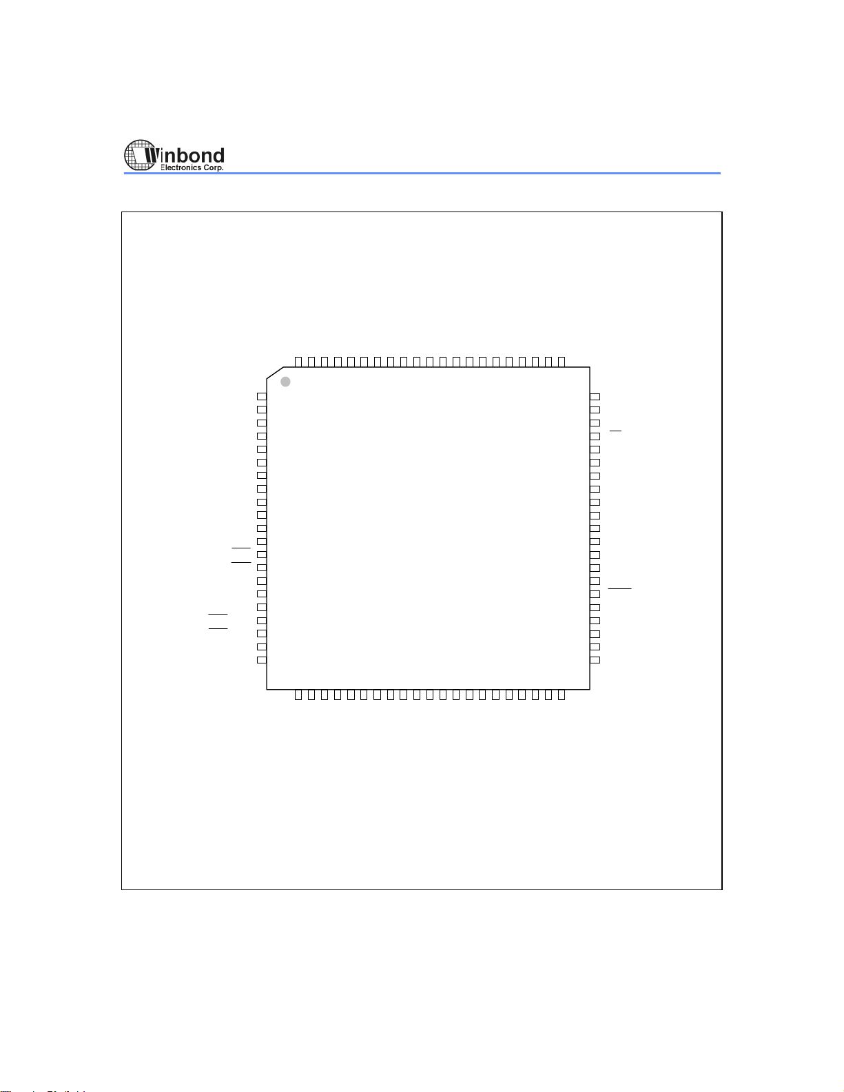
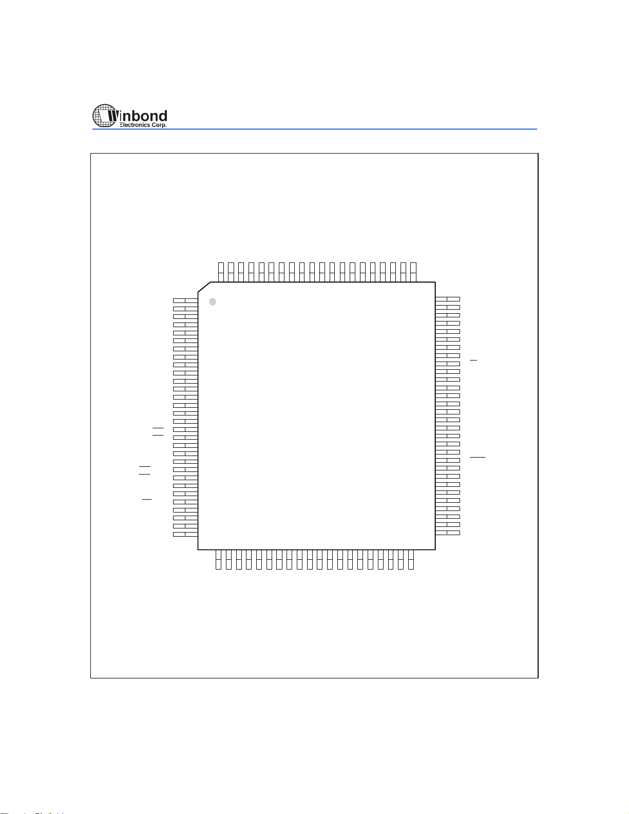
PIN CONFIGURATIONS
12
P1.5
13
P1.6
14
P1.7
P8.0
P8.1
P8.2
P8.3
P8.4
P8.5
P8.6
P8.7
INT3
INT2
VDD
15
16
17
18
19
20
21
22
23
24
25
26
27
28
29
30
31
32
RESET
RXD, P3.0
TXD, P3.1
INT0, P3.2
INT1, P3.3
T0, P3.4
T1, P3.5
P
1
.
4
1
333435363738394
1
4
1
1
1
.
N
.
.
.
.
3
0
C
7
0
1
2
8911
567
D
P
P
P
P
P
D
P
P
4
4
.
.
5
6
4
3
P
P
P
P
P
4
4
4
4
4
.
.
3
4
12
N
.
.
.
1
0
C
2
8
4
3
D
D
D
D
D
D
W78C438CP
84-pin PLCC
4142434445464748495
0
W78C438C
P
P
P
P
0
V
.
D
0
D
8081828
9
P
0
0
0
0
.
.
.
.
1
2
3
4
7677787
7
5
74
P0.5
73
P0.6
72
P0.7
71
EA
70
AP5.0
69
AP5.1
68
AP5.2
67
AP5.3
66
AP5.4
65
AP5.5
64
AP5.6
63
AP5.7
62
61
60
59
58
57
56
55
525
54
3
5
1
0
DD
V
SS
V
ALE
PSEN
P2.7
P2.6
P2.5
P2.4
P2.3
P
X
P
3
T
3
.
A
.
7
L
6
,
2
,
/
/
R
W
D
R
A
A
A
A
A
A
A
A
A
A
X
V
N
T
S
P
P
C
A
S
L
1
P
P
P
P
7
7
7
.
.
.
3
2
1
,
,
,
/
/
/
C
C
C
S
S
S
3
2
1
P
7
6
6
6
.
.
.
.
0
7
6
5
,
/
C
S
0
A
P
P
P
P
6
6
6
6
.
.
.
.
4
3
2
1
P
A
P
P
2
P
2
2
.
6
.
.
2
.
0
1
0
- 2 -
Page 3
Pin Configurations, continued
W78C438C
T
2
T
E
2
X
,
,
P
P
P
P
1
1
1
1
N
C
.
.
.
.
3
2
1
4
D
D
D
D
P
P
P
P
P
1
4
4
4
4
.
.
.
.
.
0
6
7
4
5
D
D
D
D
P
P
P
P
P
4
4
4
4
V
.
.
.
.
D
0
2
3
1
D
P
P
P
0
0
0
0
.
0
N
.
.
.
C
3
1
2
NC
NC
NC
NC
P1.5
P1.6
P1.7
RESET
P8.0
P8.1
P8.2
P8.3
P8.4
P8.5
P8.6
P8.7
INT3
INT2
RXD, P3.0
VDD
TXD, P3.1
INT0, P3.2
INT1, P3.3
T0, P3.4
T1, P3.5
WR, P3.6
1
0
9
0
1
2
3
4
5
6
7
8
9
10
11
12
13
14
15
16
17
18
19
20
21
22
23
24
25
26
NC
NC
NC
NC
27
28
29
30
333
P
X
X
3 .
T
T
7 ,
A
A
/
L
L
R
2
1
D
333637833904
345
V
S
S
456786512
W78C438CF
100-pin PQFP
A
N
A
A
P
C
P
P
7
7
7
.
.
.
3
1
2
,
,
,
/
/
/
C
C
C
S
S
S
3
1
2
9
3
4
444444 445
123 45 6 78
A
A
A
A
P
P
P
P
6
6
6
7
.
.
.
.
5
6
7
0
,
/
C
S
0
89012
7
A
A
A
A
A
P
P
P
P
P
6
6
6
6 .
6
.
.
.
0
.
3
4
2
1
888888888999999999
4
3
P
2
.
0
80
79
78
77
76
75
74
73
72
71
70
69
68
67
66
65
64
63
62
61
60
59
58
57
56
55
54
53
52
51
9
012
P
P
2
2
.
.
1
2
NC
NC
NC
NC
P0.4
P0.5
P0.6
P0.7
EA
AP5.0
AP5.1
AP5.2
AP5.3
AP5.4
AP5.5
AP5.6
AP5.7
DD
V
SS
V
ALE
PSEN
P2.7
P2.6
P2.5
P2.4
NC
NC
NC
NC
P2.3
Publication Release Date: July 1998
- 3 - Revision A1
Page 4
W78C438C
PIN DESCRIPTION
P0.0−P0.7 I/O Port 0
These pins function the same as those in the W78C32, except that a multiplexed address/data bus is
not provided during accesses to external memory.
P1.0−P1.7 I/O Port 1
Functions are the same as in the W78C32.
P2.0−P2.7 I/O Port 2
Functions are the same as in the W78C32, except that an upper address bus is not provided during
accesses to external memory.
−
P3.7 I/O Port 3
P3.0
Functions are the same as in the W78C32.
DP4.0−DP4.7 Data/Address Bus
DP4 provides multiplexed low-byte address/data during access to external memory.
AP5.0−AP5.7 Address Bus
AP5 outputs the <7:0> address of the external ROM multiplexed with the <7:0> address of the
external data RAM.
AP6.0−AP6.7 Address Bus
AP6 outputs the <15:8> address of the external ROM multiplexed with the <15:8> address of the
external data RAM. During the execution of "MOVX @Ri," the output of AP6 comes from the HB
register, which is the page register for the high byte address, and its address is 0A1H.
AP7.0−AP7.3 Address Bus/Chip Select Pins
Set bit 7 of the EPMA (Extended Program Memory Address) register to determine the functions of
port 7. When this bit is "0" (default value), AP7 allows the external memory data to be accessed by
outputting the <19:16> address of the external memory from bits<3:0> of the EPMA register during
the execution of "MOVC A, @A+DPTR" or "MOVX dest, src." At all other times, AP7<3:0> will output
0H.
When this bit is "1," AP7<3:0> (CS3−0) are the chip select pins, which support memory-mapped
peripheral device select, and only one pin is active low at any one time. These pins are decoded by
AP6<7:6>. For details, see the table below.
AP6.7 AP6.6 DESCRIPTION
0 0 AP70: low; others: high
0 1 AP71: low; others: high
1 0 AP72: low; others: high
1 1 AP73: low; others: high
- 4 -
Page 5
W78C438C
INT2
INT3
EA
PSEN
P8.0−P8.7 I/O Port
Functions are the same as those of Port 1 in the W78C31, except that they are mapped by the P8
register and not bit-addressable. The P8 register is not a standard register in the W78C32. Its address
is at 0A6H.
,
External Interrupt, Input
Functions are similar to those of external INT0 , INT1 in the W78C32, except that the functions/status
of these interrupts are determined/shown by the bits in the XICON (External Interrupt Control)
register. The XICON register is bit-addressable but is not a standard register in the W78C32. Its
address is at 0C0H. For details, see the Functional Description below.
External Address, Input
Functions same as W78C32.
RST, XTAL1, XTAL2,
Functions same as W78C32.
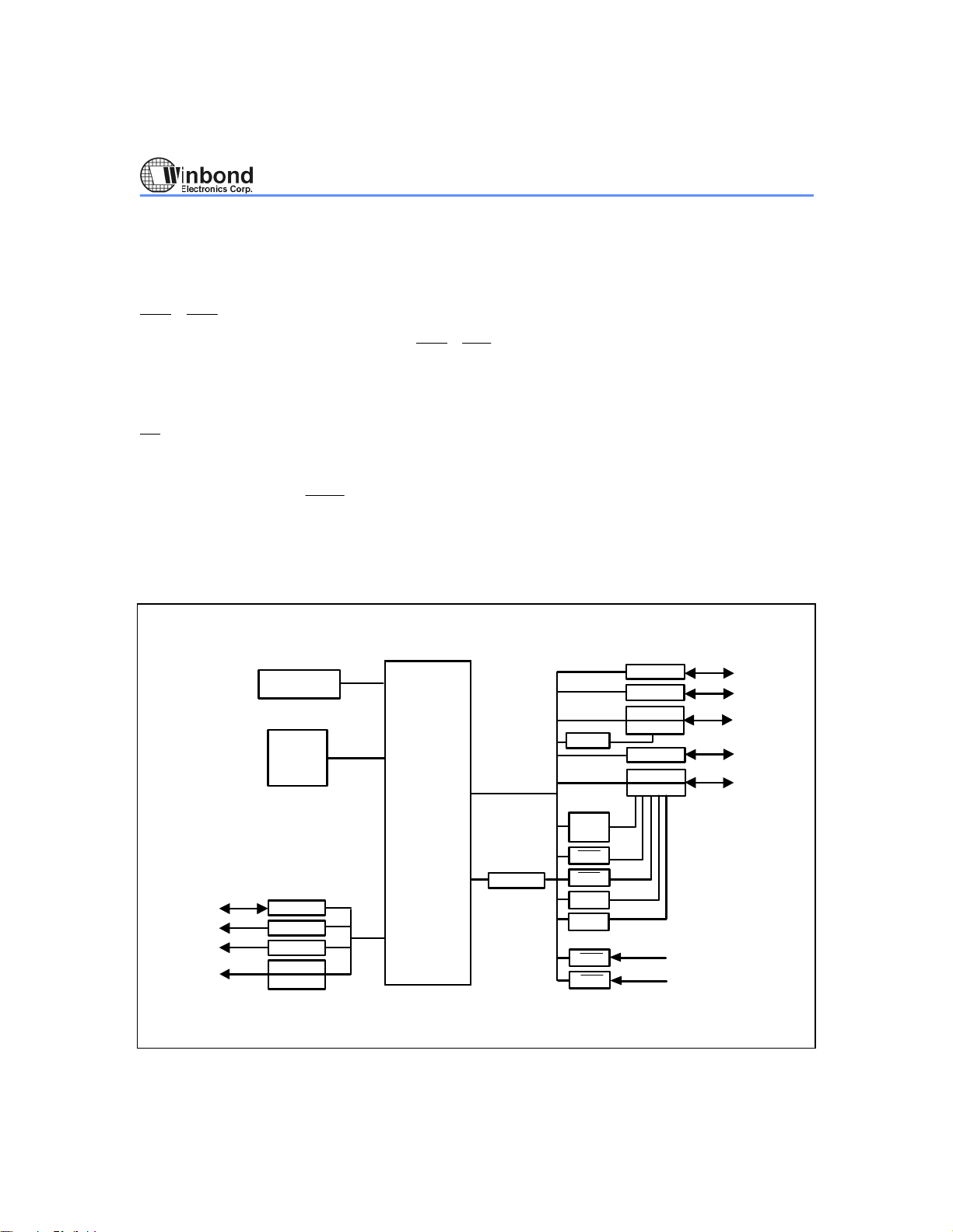
BLOCK DIAGRAM
SFR
RAM
256
Bytes
DP4
AP5
AP6
AP7
Alternate
, ALE
CPU
CORE
Data Bus
Interrupt
Timer2
Serial
Port
INT0
INT1
Timer0
Timer1
INT2
INT3
Port 8
Port 0
Port 1
Alternate
Port 2
Port 3
Alternate
Publication Release Date: July 1998
- 5 - Revision A1
Page 6

W78C438C
FUNCTIONAL DESCRIPTION
The W78C438C is a functional extension of the W78C58 microcontroller. It contains a 256 × 8 RAM,
64 KB program/1 MB data memory address or memory-mapped chip select logic, two 8-bit address
ports, one 8-bit data port, five general I/O ports, four external interrupts, three timers/counters, and
one serial port.
Dedicated Data and Address Port
The W78C438C provides four general-purpose I/O ports for W78C32 applications; the address and
data bus are separated from Port 0 and Port 2 so that these ports can be used as general-purpose I/O
ports. In this product, DP4 is the data bus for external ROM and RAM, AP5<7:0> are the low byte
address, AP6<7:0> are the high byte address,
WR ) and P3.7 (RD ) are the write/read control signals for the external RAM. The external latch for
(
multiplexing the low byte address is no longer needed in this product. The W78C438C uses AP5 and
AP6 to support 64 KB external program memory and 64 KB external data memory, just as a standard
W78C32 does.
The W78C438C provides four pins, AP7.3−AP7.0 (CS3−CS0), to support either 64 KB program/1 MB
data memory space or memory-mapped chip select logic. Bit 7 of the EPMA (Extended Program
Memory Address) register, which is described in Table 1 below, determines the functions of these
pins.
When this bit is "0" (the default value), AP7<3:0> support external program/data memory addresses
up to 64 KB/1 MB for applications which need additional external memory to store large amounts of
data.
Although there is 1M bytes memory space, instructions stored here can not be run at full range of this
area except the first 64 Kbytes. It is owing to the fact that during the instruction fetch cycle, AP7<3:0>
always output 0s to address lines A19−A16. This limits the program code to store at address 0−
0FFFFH (64K). The rest of the area (10000H−FFFFFH) can be treated as ROM data storage which
can be read by "MOVC A, @A+DPTR" instruction.
When "MOVC A, @A+DPTR" is executed to read the external ROM data or "MOVX dest, src" is
executed to access the external RAM data, AP7<3:0> output address <19:16> from bits <3:0> of the
EPMA (Extended Program Memory Address) register. At other times, AP7<3:0> always output 0H to
ensure the instruction fetch is within the 64K program memory address. Different banks can be
selected by modifying the content of the EPMA register before the execution of "MOVC A,
@A+DPTR" or "MOVX dest, src."
[Example]. Access the external ROM/RAM data from external memory space.
CLR A ; Clear Accumulator.
MOV DPTR, #0H ; Clear DPTR.
MOV 0A2H, #02 ; Initialize EPMA(0A2H). EPMA.7 = 0: extended memory space
; EPMA.<3:0> = 0010B, the address range: 20000−2FFFFH.
MOVC A, @A+DPTR ; Read the external ROM data from location 20000H.
MOVX A, @DPTR ; Read the external RAM data from location 20000H.
CLR A
MOV 0A2H, #03H ; EPMA.<3:0> = 0011B, the address range: 30000H−3FFFFH.
MOVC A, @A+DPTR ; Read the external ROM data from location 30000H.
MOVX @DPTR, A ; Write the contents of Accumulator to external RAM data.
; location 30000H.
PSEN enables the external ROM to DP4, and P3.6
- 6 -
Page 7

(A) EPMA.7 = 0
W78C438C
EPROM
W78C438
P0
P1
P2
P8
INT0
INT1
INT2
INT3
RD
WR
AP5
AP6
AP7
DP4
PSEN
P3
\ 8
\ 8
\ 4
\ 8
ADDR (20-bit)
64K PROGRAM
DATA AREA
OE
RAM
ADDR 1MB
(20-bit)
DATA
WE
OE
When bit 7 of the EPMA is "1," AP7<3:0> are the output pins that support memory-mapped peripheral
chip select logic, which eliminates the need for glue logic. These pins are decoded by AP6<7:6>.
Only one pin is active low at any time. That is, they are active individually with 16K address
resolution. For example, CS0 is active low in the address range from 0000H to 3FFFH, CS1 is active
low in the address range from 4000H to 7FFFH, and so forth.
(B) EPMA.7 = 1
W78C438
P0
P1
P2
P8
INT0
INT1
INT2
INT3
RD
WR
ADDR (16-bit)
AP5
AP6
DP4
PSEN
\ 8
\ 8
\ 8
\ 8
\ 6
P3
AP7.0
AP7.1
AP7.2
AP7.3
EPROM
64K PROGRAM
DATA AREA
OE
RAM
ADDR (14-bit)
0000h
DATA
3FFFh
(16k)
WE
OE
Device
4000h
7FFFh
(16k)
Device
8000h
BFFFh
(16k)
Device
C000h
FFFFh
(16k)
Publication Release Date: July 1998
- 7 - Revision A1
Page 8

W78C438C
The EPMA register is a nonstandard 8-bit SFR at address 0A2H in the standard W78C32. To
read/write the EPMA register, one can use the "MOV direct" instruction or "read-modify-write"
instructions. Bits <6:4> of the EPMA register are reserved bits, and their output values are 111B if
they are read. The content of EPMA is 70H after a reset. The EPMA register does not support bitaddressable instructions.
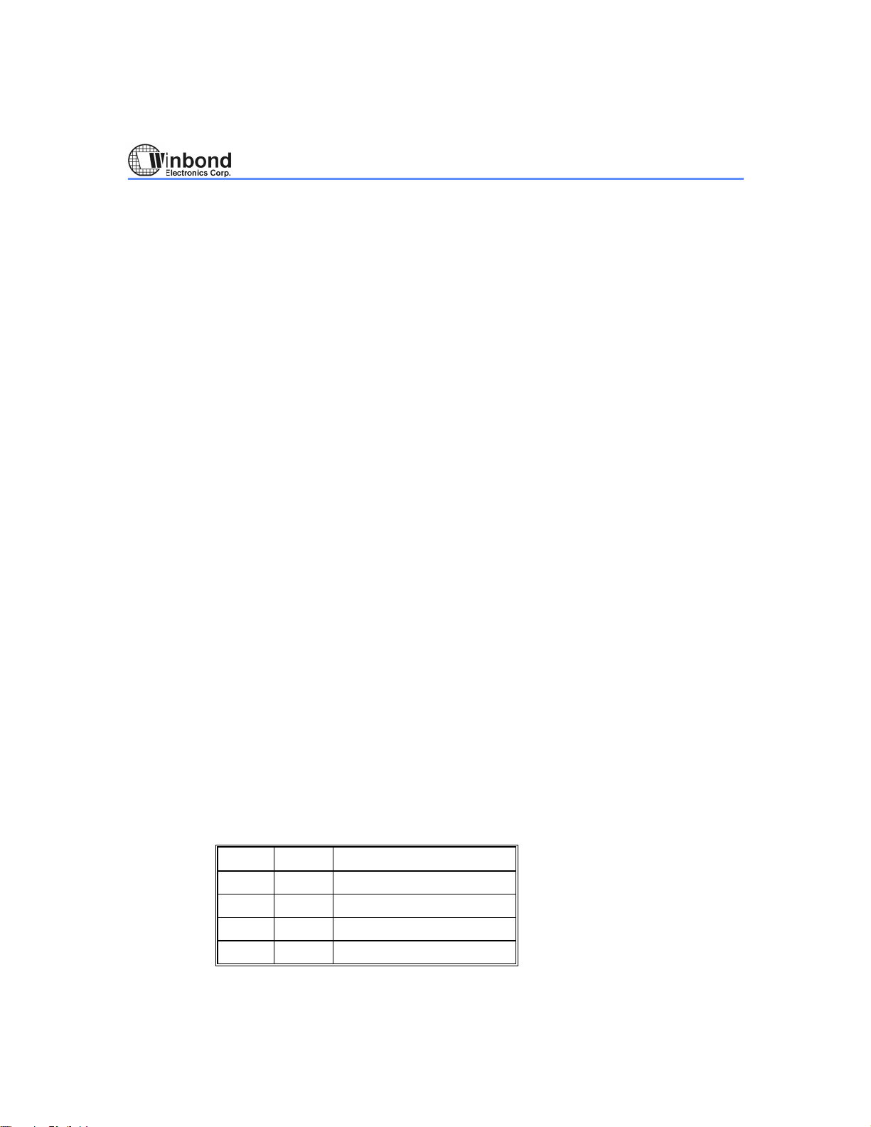
BIT NAME FUNCTION
7 EPMA7 EPMA7 = 0: 64 KB program/1 MB data memory space mode
EPMA7 = 1: memory-mapped chip select mode
6 EPMA6 Reserved
5 EPMA5 Reserved
4 EPMA4 Reserved
3 EPMA3 Value of AP7.3
2 EPMA2 Value of AP7.2
1 EPMA1 Value of AP7.1
0 EPMA0 Value of AP7.0
Table 1. Functional Description of EPMA Register
Additional I/O Port
The W78C438C provides one parallel I/O port, Port 8. Its function is the same as that of Port 1 in the
W78C31, except that it is mapped by the P8 register and is not bit-addressable. The P8 register is not
a standard register in the standard W78C32. Its address is at 0A6H. To read/write the P8 register, one
can use the "MOV direct" instruction or "read-modify-write" instructions.
[Example]: MOV 0A6H, A ; Output data via Port 8.
MOV A, 0A6H ; Input data via Port 8.
Additional External Interrupt
The W78C438C provides two additional external interrupts,
similar to those of external interrupts 0 and 1 in the W78C32. The functions (or the status) of these
interrupts are determined by (or shown by) the bits in the XICON (External Interrupt Control) register.
For details, see Table 2. The XICON register is bit-addressable but is not a standard register in the
standard 80C32. Its address is at 0C0H. To set/clear the bit of the XICON register, one can use the
"SETB(
vector addresses and the priority polling sequence within the same level are shown in Table 3.
[Example].
CLR) bit" instruction. For example, "SETB 0C2H" sets the EX2 bit of XICON. The interrupt
SETB 0C0H ;
SETB 0C3H ;
SETB 0C2H ; Enable
CLR 0C4H ;
INT2 is falling-edge triggered.
INT2 is high-priority.
INT2 .
INT3 is low-level triggered.
INT2 and INT3 , whose functions are
- 8 -
Page 9

W78C438C
BIT ADDR. NAME FUNCTION
7 0C7H PX3
6 0C6H EX3
High/low priority level for
Enable/disable interrupt from
5 0C5H IE3 If IT3 is "1," IE3 is set/cleared automatically by hardware when interrupt is
detected/serviced.
4 0C4H IT3
3 0C3H PX2
2 0C2H EX2
INT3 is falling-edge/low-level triggered when this bit is set/cleared by software.
High/low priority level for
Enable/disable interrupt from
1 0C1H IE2 If IT2 is "1," IE2 is set/cleared automatically by hardware when interrupt is
detected/serviced.
0 0C0H IT2
INT2 is falling-edge/low-level triggered when this bit is set/cleared by software.
Table 2. Functions of XICON Register
INTERRUPT SOURCE VECTOR ADDRESS PRIORITY SEQUENCE
External Interrupt 0 03H 0 (Highest)
Timer/Counter 0 0BH 1
External Interrupt 1 13H 2
Timer/Counter 1 1BH 3
Serial Port 23H 4
Timer/Counter 2 2BH 5
External Interrupt 2 33H 6
External Interrupt 3 3BH 7 (Lowest)
Table 3. Priority of Interrupts
INT3 is specified when this bit is set/cleared by software.
INT3 when this bit is set/cleared by software.
INT2 is specified when this bit is set/cleared by software.
INT2 when this bit is set/cleared by software.
Newly Added Special Function Registers
The W78C438C uses four newly defined special function registers, which are described in Table 4. To
read/write these registers, use the "MOV direct" or "read-modify-write" instructions.
REGISTER ADDR. FUNCTION LENGTH R/W
1 HB A1H During the execution of "MOVX @Ri," the content of HB is output to
2 EPMA A2H EPMA.7 determines functions of AP7.
3 P8 A6H The content of P8 is output to port 8. 8 R/W 0FFH
4 XICON C0H
AP6.
EPMA.3−EPMA.0 determine values of AP7<3:0> when EPMA.7 is
"0."
The bits of XICON determine/show the functions/status of
. Bit-addressable.
INT3
Table 4. Newly Added Special Function Registers of the W78C438C
INT2 −
8 R/W 00H
8 R/W 70H
8 R/W 00H
Publication Release Date: July 1998
- 9 - Revision A1
TYPE
VALUE
AFTER
RESET
Page 10
W78C438C
Notes:
1. The instructions used to access these nonstandard registers may cause assembling errors with respect to the 2500 A. D.
assembler, but these errors can be ignored by adding directive ".RAMCHK OFF" ahead these instructions.
2. In the newly added SFR of W78C438C, only XICON register is bit-addressable.
Power Reduction Function
The W78C438C supports power reduction just as the W78C32 does. The following table shows the
status of the external pins during the idle and power-down modes.
FUNCTION
ALE,
PSEN
P0
−
P3, P8
DP4 AP5, AP6 AP7
Idle 1 1 Port Data Floating Address Note
Power Down 0 0 Port Data Floating Address Note
Note: AP7 is either 0 or a value decoded by AP6<7:6>, depending on the value of EPMA.7.
Programming Difference
The W78C438C is programmed in the same way as the W78C32, except that the external data RAM
is accessed by a "MOVX @Ri" instruction. To support address paging, there is an additional 8-bit SFR
"HB" (high byte), which is a nonstandard register, at address 0A1H. During execution of the "MOVX
@Ri" instruction, the contents of HB are output to AP6. The page address is modified by loading the
HB register with a new value before execution of the "MOVX @Ri" instruction. To read/write the HB
register, one can use the "MOV direct" instruction or "read-modify-write" instructions. The HB register
does not support bit-addressable instructions.
[Example]. MOV R1, #0H ; R1 = 0.
MOV 0A1H, #0FFH ; HB contents FFH.
MOVX A, @R1 ; Read the contents of external RAM location FF00H into
; Accumulator.
MOV 0A1H, #12H ; HB contents 12H.
MOVX @R1, A ; Copies the contents of Accumulator into external RAM
; location 1200H.
ABSOLUTE MAXIMUM RATINGS
PARAMETER SYMBOL MIN. MAX. UNIT
DC Power Supply
V
DD−VSS
Input Voltage VIN VSS -0.3 VDD +0.3 V
Operating Temperature TOPR 070
Storage Temperature TSTG -55 +150
Note: Exposure to conditions beyond those listed under Absolute Maximum Ratings may adversely affect the life and reliability of the
device.
- 10 -
-0.3 +7.0 V
°C
°C
Page 11

W78C438C
DC CHARACTERISTICS
VDD−VSS = 5V ±10%, TA = 25° C, FOSC = 20 MHz, unless otherwise specified.
PARAMETER SYM. TEST CONDITIONS MIN. TYP. MAX. UNIT
Oper. Voltage VDD 4.5 5 5.5 V
Oper. Current IDD * No load - - 20 mA
Idle Current IIDLE Program idle mode - - 7 mA
Pwdn Current IPWDN Program power-down mode - - 50
Input Leakage
Current
Input Leakage
Current
Input Leakage
Current
Input Leakage
Current
Output Low Voltage VOL1 IOL1 = 2 mA (Port 1, 2, 3, 8) - - 0.45 V
Output High Voltage VOH1
Output Low Voltage VOL2 IOL2 = 4mA Note 3
Output High Voltage VOH2
Output Low Voltage VOL3 IOL2 = 2 mA (AP5, AP6, AP7) - - 0.45 V
Output High Voltage VOH3
Input Voltage VILT
Input Voltage VIHT
Input Voltage VILC
Input Voltage VIHC
Input Voltage VILR
Input Voltage VIHR
ILK1
INT2 , INT3
-300 - +10
Internal pull-high Notes 1, 2
ILK2 RESET
Internal pull-low
ILK3
EA , Port 0, DP4 Note 1
Notes 1, 2
-10 - +300
-10 - +10
ILK4 P1, P2, P3, P8 Note 1 -50 - +10
IOH1 = -100 µA (Port 1, 2, 3, 8)
2.4 - - V
- - 0.45 V
(ALE, PSEN, P0, DP4)
IOH2 = -400 µA Note 3
2.4 - - V
(ALE, PSEN, P0, DP4)
IOH2 = -100 µA (AP5, AP6, AP7)
VDD = 5V ±10%
VDD = 5V ±10%
VDD = 5V ±10%, XTAL1 Note 5
VDD = 5V ±10%, XTAL1 Note 5
VDD = 5V ±10%, RESET Note 5
VDD = 5V ±10%, RESET Note 5
2.4 - - V
0 - 0.8 V
2.4 -
Note 4
0 - 0.8 V
3.5 -
Note 4
0 - 0.8 V
2.4 -
Note 4
µA
µA
µA
µA
µA
V
V
V
Notes:
IN < VDD, for INT2 , INT3 , RESET, EA , Port 0, DP4, P1, P2, P3 and P8 inputs in leakage.
1. 0 < V
2. Using an internal pull low/high resistor (approx. 30K).
3. ALE,
PSEN , P0 and DP4 in external program or data access mode.
4. The maximum input voltage is V
5. XTAL1 is a CMOS input and RESET is a Schmitt trigger input.
DD +0.2V.
- 11 - Revision A1
Publication Release Date: July 1998
Page 12
W78C438C
AC CHARACTERISTICS
AC specifications are a function of the particular process used to manufacture the product, the ratings
of the I/O buffers, the capacitive load, and the internal routing capacitance. Most of the specifications
can be expressed in terms of multiple input clock periods (T
experience less than a ±20 nS variation.
Clock Input Waveform
PARAMETER SYMBOL MIN. TYP. MAX. UNIT NOTES
Operating Speed FOP 0 - 40 MHz 1
Clock Period TCP 25 - - nS 2
Clock High TCH 10 - - nS 3
Clock Low TCL 10 - - nS 3
Notes:
1. The clock may be stopped indefinitely in either state.
2. The T
CP specification is used as a reference in other specifications.
3. There are no duty cycle requirements on the XTAL1 input.
CP), and actual parts will usually
Program Fetch Cycle
PARAMETER SYMBOL MIN. TYP. MAX. UNIT
T
Address Valid to PSEN Low
PSEN Low to Data Valid
APL 2 TCP --nS
T
PDV --2 TCP nS
Data Memory Read/Write Cycle
PARAMETER SYMBOL MIN. TYP. MAX. UNIT
T
Address Valid to RD Low
RD Low to Data Valid
Data Hold After RD High
RD Pulse Width
Address Valid to WR Low
Data Valid to WR Low
Data Hold After WR High
WR Pulse Width
Note: "∆" (due to buffer driving delay and wire loading) is 20 nS.
ARL 4 TCP -
T
RDV --4 TCP nS
T
RDQ 0-2 TCP nS
T
RS
T
AWL 4 TCP -
T
DWL 1 TCP --nS
T
WDQ 1 TCP --nS
T
WS
6 TCP -∆
6 TCP -∆
4 T
CP +∆
CP -nS
6 T
4 T
CP +∆
CP -nS
6 T
nS
nS
- 12 -
Page 13
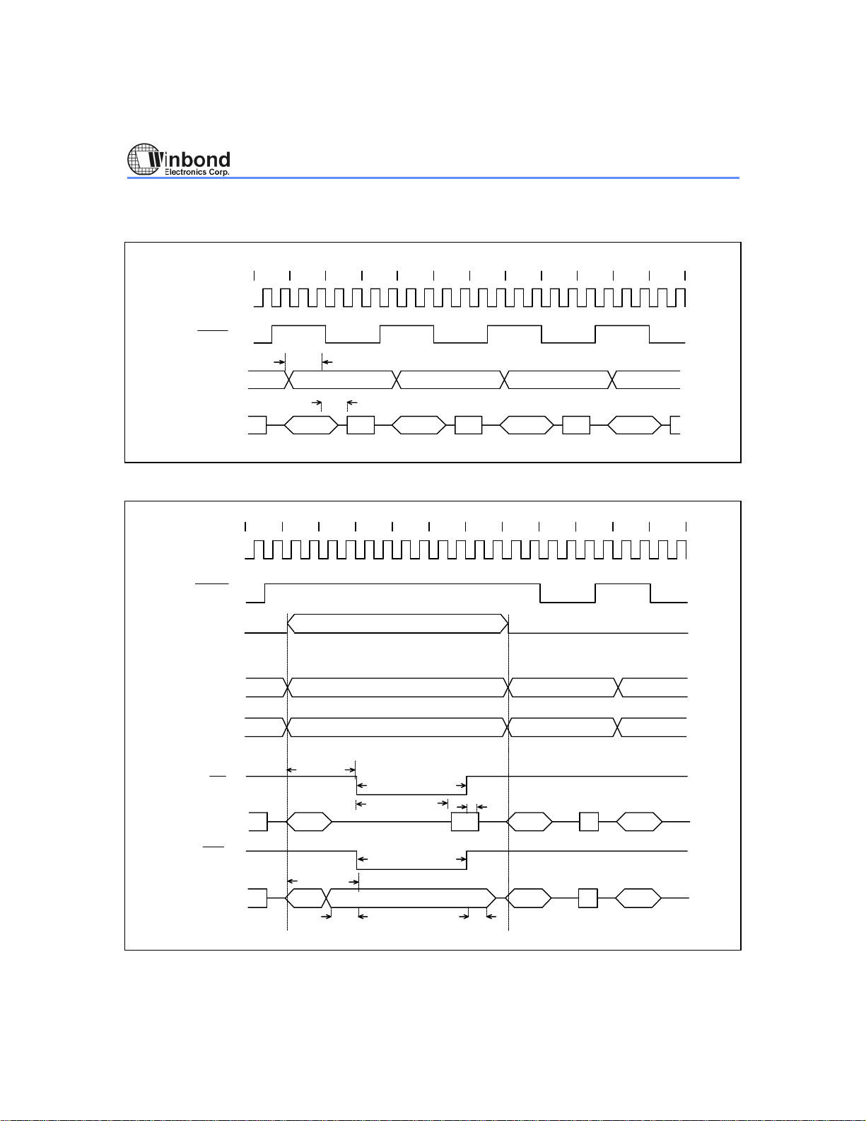
TIMING WAVEFORMS
Program Fetch Cycle
W78C438C
S1 S2
XTAL1
PSEN
T
APL
AP6<7:0>
AP5<7:0>
DP4<7:0>
T
PDV
address
address
Data Memory Read/Write Cycle
XTAL1
PSEN
AP7<3:0>
(When bit7 of EPMA is 0.)
AP6<7:0>
addr <19:16> out
DPH or HB SFR out
S3 S4 S5 S6 S1 S2 S3 S4 S5 S6
code
S1 S2 S3S8 S9 S10 S11 S12S4 S5 S6 S7
PGM address
AP5<7:0>
RD
DP4<7:0>
WR
DP4<7:0>
T
T
addr.
T
addr.
DWL
DPL or Ri out
ARL
AWL
T
RS
T
RDV
T
WS
DATA OUT
PGM address
T
RDQ
T
WDQ
addr.
data
Publication Release Date: July 1998
- 13 - Revision A1
Page 14

TYPICAL APPLICATION CIRCUITS
Using 128K × 8 bit External EPROM (W27E010)
888888889999999991
0
0
P
P
N
P
C
1
1
.
.
3
4
1
NC
2
NC
3
NC
NC
4
5
P1.5
6
P1.6
7
10 U
5 V
8.2 K
P1.7
8
RESET
9
P8.0
P8.1
10
11
P8.2
12
P8.3
13
P8.4
14
P8.5
15
P8.6
16
P8.7
17
INT3
18
INT2
19
P3.0, RXD
20
VDD
21
P3.1, TXD
22
P3.2, INT0
23
P3.3, INT1
24
P3.4, T0
25
P3.5, T1
26
P3.6, WR
NC
27
28
NC
NC
29
NC
30
P
3
.
7
X
,
T
/
A
R
L
D
2
333
X
T
A
V
SSN
L
1
3336378339044
345
D
P
P
P
1
1
1
.
4
.
.
0
1
.
2
7
W78C438C
A
A
A
P
P
P
7
7
7
.
.
.
1
2
3
,
,
,
/
/
/
C
C
C
S
S
S
1
2
3
C
D
P
4
.
6
A
P
7
.
0
,
/
C
S
0
890123456789
7
D
D
D
D
D
D
P
4
.
5
A
P
6
.
7
P
P
P
P
P
4
4
4
4
4
.
.
.
.
.
0
1
2
3
4
A
A
A
A
P
P
P
P
6
6
6
6
.
.
.
.
5
4
3
6
444444445
12345 6 78
A
P
6
.
2
65
V
D
D
A
P
6
.
1
89
1234
P
P
P
P
N
0
0
0
0
C
.
.
.
.
0
1
2
3
80
NC
79
NC
78
NC
77
NC
76
P0.4
75
P0.5
74
P0.6
P0.7
73
72
EA
71
AP5.0
70
AP5.1
69
AP5.2
68
AP5.3
67
AP5.4
66
AP5.5
65
AP5.6
64
AP5.7
63
VDD
62
VSS
61
ALE
60
PSEN
59
P2.7
P2.6
58
P2.5
57
56
P2.4
55
NC
54
NC
53
NC
NC
52
P2.3
51
A
P
P
P
P
6
2
2
2
.
.
.
.
0
2
1
0
9
012
GND
W78C438C
12
A0
11
A1
10
A2
9
A3
8
A4
7
A5
6
A6
5
A7
27
A8
26
A9
23
25
4
28
29
3
2
22
24
W27E010
A10
A11
A12
A13
A14
A15
A16
CE
OE
O0
O1
O2
O3
O4
O5
O6
O7
PGM
Vpp
Vcc
Vss
13
14
15
17
18
19
20
21
1
32
31
16
R
C1
C2
Figure A
- 14 -
Page 15

CRYSTAL C1 C2 R
16 MHz 30P 30P
24 MHz 15P 15P
33 MHz 10P 10P 6.8K
40 MHz 5P 5P 6.8K
Notes:
1. For C1, C2, R components refer to Figure A.
2. It is recommended that the crystals be replaced with oscillators for applications above 35 MHz.
Above table shows the reference values for crystal applications.
PACKAGE DIMENSIONS
84-pin PLCC
H
D
11 84
12
32
33 53
Seating Plane
D
e
b
G
D
751
74
E
H
E
54
Symbol
A
1
A
2
A
b
1
b
E
c
D
E
e
D
G
E
G
D
H
E
H
L
y
θ
Notes:
1. Dimension D & E do not include interlead
flash.
2. Dimension b1 does not include dambar
protrusion/intrusion.
A
2A
A
y
3. Controlling dimension: Inches
4. General appearance spec. should be based
on final visual inspection spec.
−
−
Dimension in inches
Nom.
Min.
0.020
0.143
0.148
0.026
0.028
0.016
0.018
0.006
0.008
1.148
1.153
0.050
0.044 0.056
1.095
1.115
1.095
1.180
1.190
1.180
1.190
0.090
0.100
0
W78C438C
Dimension in mm
Nom.
Max. Max.
Min.
0.185
0.153
0.032
0.022
0.012
1.158
1.1581.1531.148
1.135
1.1351.115
1.200
0.110
0.004
10
29.17
27.81
29.98
29.981.200
4.70
0.51
3.63
3.76
3.89
0.66
0.81
0.71
0.56
0.41
0.46
0.15
0.20
0.30
29.29
29.41
29.4129.2929.17
1.27
1.12 1.42
28.32
28.83
28.8328.3227.81
30.23
30.48
30.48
30.23
2.54
2.79
2.29
0.10
0
10
Publication Release Date: July 1998
- 15 - Revision A1
Page 16

Package Dimensions, continued
100-pin QFP
H
D
D
1
30
e b
Seating Plane
See Detail F
W78C438C
81100
Dimension in inches Dimension in mm
80
E
H
E
51
5031
c
AA
2
A
1
y
θ
L
L
1
Detail F
Symbol
Min. Nom. Max. Max.Nom.Min.
A
0.004
1
A
0.107
A
2
0.010
b
0.004
c
0.546
D
0.782
E
0.020
e
0.728
D
H
0.964
E
H
0.039
L
0.087
1
L
y
θ
Notes:
1. Dimension D & E do not include interlead
flash.
2. Dimension b does not include dambar
protrusion/intrusion.
3. Controlling dimension: Millimeters
4. General appearance spec. should be based
on final visual inspection spec.
0.130
0.10
2.718
0.117
0.112
0.012
0.006 0.152
0.551
0.787
0.026
0.740
0.976
0.047
0.095
0.254
0.016
0.101
0.010
13.87
0.556
19.87
0.792
0.498 0.802
0.032
0.752
18.49
24.49 24.80 25.10
0.988
0.055
0.991
0.103
2.21
0.004
120
0
2.845
0.305
14.00
20.00
0.65
18.80
1.194
2.413
3.30
2.972
0.407
0.254
14.13
20.13
19.10
1.397
2.616
0.102
12
Headquarters
No. 4, Creation Rd. III,
Science-Based Industrial Park,
Hsinchu, Taiwan
TEL: 886-3-5770066
FAX: 886-3-5792766
http://www.winbond.com.tw/
Voice & Fax-on-demand: 886-2-27197006
Winbond Electronics (H.K.) Ltd.
Rm. 803, World Trade Square, Tower II,
123 Hoi Bun Rd., Kwun Tong,
Kowloon, Hong Kong
TEL: 852-27513100
FAX: 852-27552064
Taipei Office
11F, No. 115, Sec. 3, Min-Sheng East Rd.,
Taipei, Taiwan
TEL: 886-2-27190505
FAX: 886-2-27197502
Note: All data and specifications are subject to change without notice.
- 16 -
Winbond Electronics North America Corp.
Winbond Memory Lab.
Winbond Microelectronics Corp.
Winbond Systems Lab.
2727 N. First Street, San Jose,
CA 95134, U.S.A.
TEL: 408-9436666
FAX: 408-5441798
 Loading...