

Page 1

Features
• High-density, High-performance, Electrically-erasable Complex
Programmable Logic Device
– 256 Macrocells
– 5 Product Terms per Macrocell, Expandable up to 40 per Macrocell
– 160, 192, 208 pins
– 10 ns Maximum Pin-to-pin Delay
– Registered Operation Up To 100 MHz
– Enhanced Routing Resources
• Flexible Logic Macrocell
– D/T/Latch Configurable Flip-flops
– Global and Individual Register Control Signals
– Global and Individual Output Enable
– Programmable Output Slew Rate
– Programmable Output Open Collector Option
– Maximum Logic Utilization by Burying a Register within a COM Output
• Advanced Power Management Features
– Automatic 3 mA Standby for “L” Version (Maximum)
– Pin-controlled 4 mA Standby Mode (Typical)
– Programmable Pin-keeper Inputs and I/Os
– Reduced-power Feature per Macrocell
• Available in Commercial and Industrial Temperature Ranges
• Available in 160-lead PQFP, 192-pin PGA, and 208-lead RQFP Packages
• Advanced EE Technology
– 100% Tested
– Completely Reprogrammable
– 10,000 Program/Erase Cycles
– 20 Year Data Retention
– 2000V ESD Protection
– 200 mA Latch-up Immunity
• JTAG Boundary-scan Testing to IEEE Std. 1149.1-1990 and 1149.1a-1993 Supported
• Fast In-System Programmability (ISP) via JTAG
• PCI-compliant
• 3.3 or 5.0V I/O Pins
• Security Fuse Feature
Highperformance
EE-based CPLD
ATF1516AS
ATF1516ASL
Preliminary
Enhanced Features
• Improved Connectivity (Additional Feedback Routing, Alternate Input Routing)
• Output Enable Product Terms
• D-latch Mode
• Combinatorial Output with Registered Feedback within Any Macrocell
• Three Global Clock Pins
• ITD (Input Transition Detection) Circuits on Global Clocks, Inputs and I/O
• Fast Registered Input from Product Term
• Programmable “Pin-keeper” Option
• V
Power-up Reset Option
CC
• Pull-up Option on JTAG Pins TMS and TDI
• Advanced Power Management Features
– Edge Controlled Power-down “L”
– Individual Macrocell Power Option
– Disable ITD on Global Clocks, Inputs and I/O
Rev. 0994D–09/99
1
Page 2
Block Diagram
6 to 12
P
O
N
M
256
E
F
G
H
L
K
J
I
2
ATF1516AS(L)
Page 3
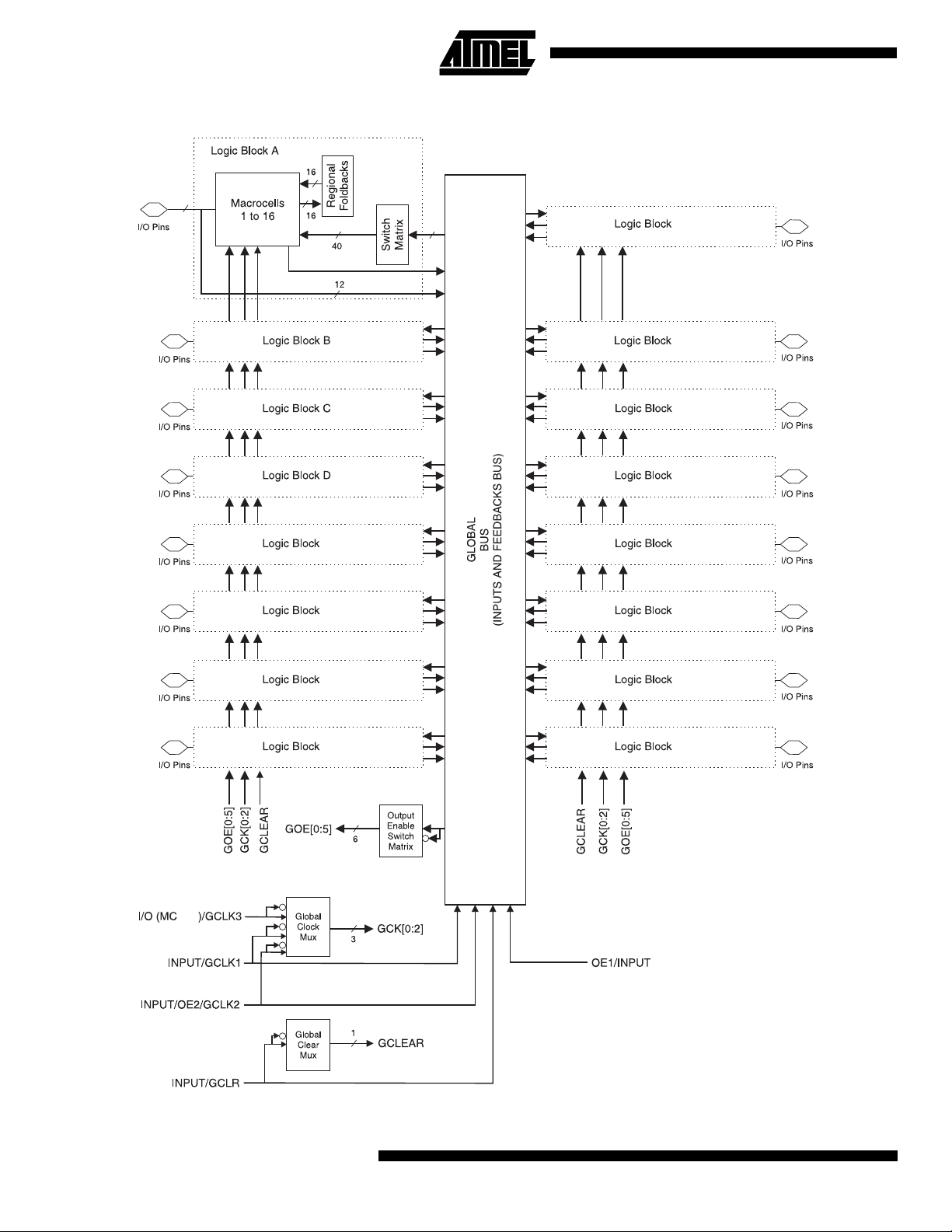
Description
ATF1516AS(L)
The ATF1516AS is a high-performance, high-density complex programmable logic device (CPLD) that utilizes
Atmel’s proven electrically-erasable technology. With 256
logic macrocells and up to 164 inputs, it easily integrates
logic from several TTL, SSI, MSI, LSI and classic PLDs.
The ATF1516AS’s enhanced routing switch matrices
increase usable gate count and increase odds of successful pin-locked design modifications.
The ATF1516AS has up to 160 bi-directional I/O pins and
four dedicated input pins, depending on the type of device
package selected. Each dedicated pin can also serve as a
global control signal, register clock, register reset or output
enable. Each of these control signals can be selected for
use individually within each macrocell.
Each of the 256 macrocells generates a buried feedback
that goes to the global bus. Each input and I/O pin also
feeds into the global bus. The switch matrix in each logic
block then selects 40 individual signals from the global bus.
Each macrocell also generates a foldback logic term that
goes to a regional bus. Cascade logic between macrocells
in the ATF1516AS allows fast, efficient generation of complex logic functions. The ATF1516AS contains eight such
logic chains, each capable of creating sum term logic with a
fan-in of up to 40 product terms
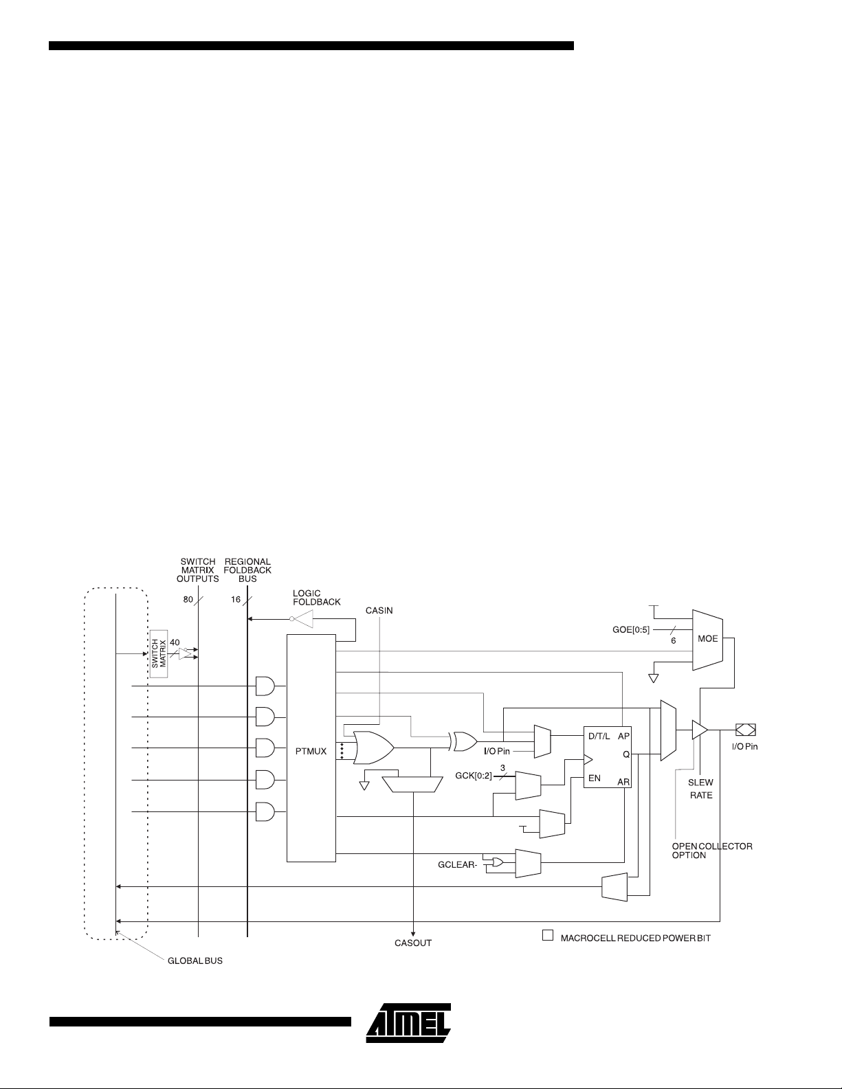
The ATF1516AS macrocell, shown in Figure 1, is flexible
enough to support highly complex logic functions operating
at high speed. The macrocell consists of five sections,
product terms and product term select multiplexer,
OR/XOR/CASCADE logic, a flip-flop, output select and
enable and logic array inputs.
Unused macrocells are automatically disabled by the compiler to decrease power consumption. A security fuse,
when programmed, protects the contents of the
ATF1516AS. Two bytes (16 bits) of User Signature are
accessible to the user for purposes such as storing project
name, part number, revision or date. The User Signature is
accessible regardless of the state of the security fuse.
The ATF1516AS device is an in-system programmable
(ISP) device. It uses the industry standard 4-pin JTAG
interface (IEEE Std. 1149.1), and is fully compliant with
JTAG’s Boundary-scan Description Language (BSDL). ISP
allows the device to be programmed without removing it
from the printed circuit board. In addition to simplifying the
manufacturing flow, ISP also allows design modifications to
be made in the field via software.
Figure 1. ATF1516AS Macrocell
3
Page 4

Product Terms and Select MUX
Each ATF1516AS macrocell has five product terms. Each
product term receives as its inputs all signals from both the
global bus and regional bus.
The product term select multiplexer (PTMUX) allocates the
five product terms as needed to the macrocell logic gates
and control signals. The PTMUX programming is determined by the design compiler, which selects the optimum
macrocell configuration.
OR/XOR/CASCADE Logic
The ATF1516AS’s logic structure is designed to efficiently
support all types of logic. Within a single macrocell, all the
product terms can be routed to the OR gate, creating a 5input AND/OR sum term. With the addition of the CASIN
from neighboring macrocells, this can be expanded to as
many as 40 product terms with little additional delay.
The macrocell’s XOR gate allows efficient implementation
of compare and arithmetic functions. One input to the XOR
comes from the OR sum term. The other XOR input can be
a product term or a fixed high or low level. For combinatorial outputs, the fixed level input allows polarity selection.
For registered functions, the fixed levels allow DeMorgan
minimization of product terms. The XOR gate is also used
to emulate T- and JK-type flip-flops.
Flip-flop
The ATF1516AS’s flip-flop has very flexible data and control functions. The data input can come from either the
XOR gate, from a separate product term or directly from
the I/O pin. Selecting the separate product term allows creation of a buried registered feedback within a combinatorial
output macrocell. (This feature is automatically implemented by the fitter software). In addition to D, T, JK and
SR operation, the flip-flop can also be configured as a flowthrough latch. In this mode, data passes through when the
clock is high and is latched when the clock is low.
The clock itself can be either the Global CLK signal (GCK)
or an individual product term. The flip-flop changes state on
the clock’s rising edge. When the GCK signal is used as
the clock, one of the macrocell product terms can be
selected as a clock enable. When the clock enable function
is active and the enable signal (product term) is low, all
clock edges are ignored. The flip-flop’s asynchronous reset
signal (AR) can be either the Global Clear (GCLEAR), a
product term, or always off. AR can also be a logic OR of
GCLEAR with a product term. The asynchronous preset
(AP) can be a product term or always off.
Output Select and Enable
The ATF1516AS macrocell output can be selected as registered or combinatorial. The buried feedback signal can be
either combinatorial or registered signal regardless of
whether the output is combinatorial or registered.
The output enable multiplexer (MOE) controls the output
enable signals. Any buffer can be permanently enabled for
simple output operation. Buffers can also be permanently
disabled to allow use of the pin as an input. In this configuration all the macrocell resources are still available,
including the buried feedback, expander and CASCADE
logic. The output enable for each macrocell can be
selected as either of the two dedicated OE input pins as an
I/O pin configured as an input, or as an individual product
term.
Global Bus/Switch Matrix
The global bus contains all input and I/O pin signals as well
as the buried feedback signal from all 256 macrocells.
The switch matrix in each logic block receives as its inputs
all signals from the global bus. Under software control, up
to 40 of these signals can be selected as inputs to the logic
block.
Foldback Bus
Each macrocell also generates a foldback product term.
This signal goes to the regional bus and is available to 16
macrocells. The foldback is an inverse polarity of one of the
macrocell’s product terms. The 16 foldback terms in each
region allow generation of high fan-in sum terms (up to 21
product terms) with little additional delay.
4
ATF1516AS(L)
Page 5

ATF1516AS(L)
Programmable Pin-keeper Option for Inputs and I/Os
The ATF1516AS offers the option of programming all input
and I/O pins so that “pin keeper” circuits can be utilized.
When any pin is driven high or low and then subsequently
left floating, it will stay at that previous high or low level.
This circuitry prevents unused input and I/O lines from
floating to intermediate voltage levels, which causes
unnecessary power consumption and system noise. The
keeper circuits eliminate the need for external pull-up resistors and eliminate their DC power consumption.
Input Diagram
I/O Diagram
To further reduce power, each ATF1516AS macrocell has
a reduced-power bit feature. This feature allows individual
macrocells to be configured for maximum power savings.
This feature may be selected as a design option.
All ATF1516AS also have an optional power-down mode.
In this mode, current drops to below 10 mA. When the
power-down option is selected, either PD1 or PD2 pins (or
both) can be used to power down the part. The powerdown option is selected in the design source file. When
enabled, the device goes into power-down when either
PD1 or PD2 is high. In the power-down mode, all internal
logic signals are latched and held, as are any enabled
outputs.
All pin transitions are ignored until the PD pin is brought
low. When the power-down feature is enabled, the PD1 or
PD2 pin cannot be used as a logic input or output. However, the pin’s macrocell may still be used to generate
buried foldback and cascade logic signals.
All power-down AC characteristic parameters are computed from external input or I/O pins, with reduced-power
bit turned on. For macrocells in reduced-power mode
(reduced-power bit turned on), the reduced-power adder,
, must be added to the AC parameters, which include
t
RPA
the data paths t
LAD
, t
LAC
, tIC, t
ACL
, t
ACH
and t
SEXP
.
Each output also has individual slew rate control. This may
be used to reduce system noise by slowing down outputs
that do not need to operate at maximum speed. Outputs
default to slow switching, and may be specified as fast
switching in the design file.
Speed/Power Management
The ATF1516AS has several built-in speed and power
management features. The ATF1516AS contains circuitry
that automatically puts the device into a low-power standby
mode when no logic transitions are occurring. This not only
reduces power consumption during inactive periods, but
also provides proportional power savings for most applications running at system speeds below 50 MHz.
Design Software Support
ATF1516AS designs are supported by several third-party
tools. Automated fitters allow logic synthesis using a variety
of high-level description languages and formats.
Power-up Reset
The ATF1516AS is designed with a power-up reset, a feature critical for state machine initialization. At a point
delayed slightly from V
crossing V
CC
initialized, and the state of each output will depend on the
polarity of its buffer. However, due to the asynchronous
nature of reset and uncertainty of how V
the system, the following conditions are required:
1. The V
rise must be monotonic,
CC
2. After reset occurs, all input and feedback setup
times must be met before driving the clock pin
high, and,
3. The clock must remain stable during T
The ATF1516AS has two options for the hysteresis about
the reset level, V
, Small and Large. During the fitting
RST
, all registers will be
RST
actually rises in
CC
.
D
5
Page 6

process users may configure the device with the Power-up
Reset hysteresis set to Large or Small. Atmel POF2JED
users may select the Large option by including the flag
“-power_reset” on the command line after “filename.POF”.
To allow the registers to be properly reinitialized with the
Large hysteresis option selected, the following condition is
added:
4. If V
When the Large hysteresis option is active, I
by several hundred microamps as well.
falls below 2.0V, it must shut off com-
CC
pletely before the device is turned on again.
is reduced
CC
Security Fuse Usage
Atmel provides ISP hardware and software to allow programming of the ATF1516AS via the PC. ISP is perfomed
by using either a download cable or a comparable board
tester or a simple microprocessor interface.
To facilitate ISP programming by the Automated Test
Equipment (ATE) vendors. Serial Vector Format (SVF)
files can be created by Atmel provided software utilities.
ATF1516AS devices can also be programmed using standard third-party programmers. With third-party
programmer, the JTAG ISP port can be disabled thereby
allowing four additional I/O pins to be used for logic.
Contact your local Atmel representatives or Atmel PLD
applications for details.
A single fuse is provided to prevent unauthorized copying
of the ATF1516AS fuse patterns. Once programmed, fuse
verify is inhibited. However, User Signature and device ID
remains accessible.
Programming
ATF1516AS devices are in-system programmable (ISP)
devices utilizing the 4-pin JTAG protocol. This capability
eliminates package handling normally required for programming and facilitates rapid design iterations and field
changes.
Timing Model
ISP Programming Protection
The ATF1516AS has a special feature that locks the device
and prevents the inputs and I/O from driving if the programming process is interrupted for any reason. The inputs and
I/O default to high-Z state during such a condition. In addition the pin-keeper option preserves the former state during
device programming.
All ATF1516AS devices are initially shipped in the erased
state thereby making them ready to use for ISP.
Note: For more information refer to the “Desigining for
In-System Programmability with Atmel CPLDs”
application note.
U
6
ATF1516AS(L)
Page 7

ATF1516AS(L)
Input Test Waveforms and Measurement Levels
rR, tF = 1.5 ns typical
Power-down Mode
The ATF1516AS includes two pins for optional pin-controlled power-down feature. When this mode is enabled,
the PD pin acts as the power-down pin. When the PD1 and
PD2 pin is high, the device supply current is reduced to
less than 3 mA. During power-down, all output data and
internal logic states are latched and held. Therefore, all
registered and combinatorial output data remain valid. Any
outputs that were in a high-Z state at the onset will remain
at high-Z. During power-down, all input signals except the
Output AC Test Loads:
(3.0V)*
(703 )*
(8060 )*
Note: *Numbers in parenthesis refer to 3.0V operating condi-
tions (preliminary).
power-down pin are blocked. Input and I/O hold latches
remain active to ensure that pins do not float to indeterminate levels, further reducing system power. The powerdown pin feature is enabled in the logic design file. Designs
using either power-down pin may not use the PD pin logic
array input. However, all other PD pin as macrocell
resources may still be used, including the buried feedback
and foldback product term array inputs.
7
Page 8

JTAG-BST Overview
The JTAG boundary-scan testing is controlled by the Test
Access Port (TAP) controller in the ATF1516AS. The
boundary-scan technique involves the inclusion of a shiftregister stage (contained in a boundary-scan cell) adjacent
to each component so that signals at component boundaries can be controlled and observed using scan testing
principles. Each input pin and I/O pin has its own boundaryscan cell (BSC) in order to support boundary-scan testing.
The ATF1516AS does not currently include a Test Reset
(TRST) input pin because the TAP controller is automatically reset at power up. The six JTAG BST modes
supported include: SAMPLE/PRELOAD, EXTEST,
BYPASS, IDCODE. BST on the ATF1516AS is implemented using the Boundary-scan Definition Language
(BSDL) described in the JTAG specification (IEEE Standard 1149.1). Any third-party tool that supports the BSDL
format can be used to perform BST on the ATF1516AS.
The ATF1516AS also has the option of using four JTAGstandard I/O pins for in-system programming (ISP). The
ATF1516AS is programmable through the four JTAG pins
using programming compatible with the IEEE JTAG Standard 1149.1. Programming is performed by using 5V TTLlevel programming signals from the JTAG ISP interface.
The JTAG feature is a programmable option. If JTAG (BST
or ISP) is not needed, then the four JTAG control pins are
available as I/O pins.
BSC consists of three capture registers or scan registers
and up to two update registers. There are two types of
BSCs, one for input or I/O pin, and one for the macrocells.
The BSCs in the device are chained together through the
capture registers. Input to the capture register chain is fed
in from the TDI pin while the output is directed to the TDO
pin. Capture registers are used to capture active device
data signals, to shift data in and out of the device and to
load data into the update registers. Control signals are generated internally by the JTAG TAP controller. The BSC
configuration for the input and I/O pins and macrocells are
shown below.
BSC Configuration Pins and Macrocells (Except JTAG TAP Pins)
JTAG Boundary-scan Cell (BSC) Testing
The ATF1516AS contains up to 160 I/O pins and four input
pins, depending on the device type and package type
selected. Each input pin and I/O pin has its own boundaryscan cell (BSC) in order to support boundary-scan testing
as described in detail by IEEE Standard 1149.1. A typical
Note: The ATF1516AS has pull-up option on TMS and TDI
pins. This feature is selected as a design option.
8
ATF1516AS(L)
Page 9

BSC Configuration for Macrocell
ATF1516AS(L)
Pin BSC
TDO
OEJ
Pin
0
1
DQ
Capture
DR
TDI
Clock
Shift
TDO
0
0
1
DQ
DQ
1
OUTJ
TDI
Shift
0
0
1
DQ
Capture
DR
DQ
Update
DR
1
Pin
Mode
Clock
Macrocell BSC
9
Page 10

PCI Compliance
The ATF1516AS also supports the growing need in the
industry to support the new peripheral component intercon-
specifications. The PCI interface calls for high current drivers, which are much larger than the traditional TTL drivers.
nect (PCI) interface standard in PCI-based designs and
PCI Voltage-to-current Curves for +5V Signaling in Pull-up Mode
point
Pull Up
-44
Current (mA)
Test Point
-178
VCC
2.4
1.4
Voltage
DC
drive point
AC drive
-2
PCI Voltage-to-current Curves for +5V Signaling in Pull-down Mode
VCC
2.2
0.55
AC drive
Voltage
DC
drive point
3.6
point
Pull Down
95
Test Point
Current (mA)
380
10
ATF1516AS(L)
Page 11

Ordering Information
ATF1516AS(L)
t
PD
(ns)
10 5 125 ATF1516AS-10QC160
15 8 100 ATF1516AS-15QC160
15 8 100 ATF1516AS-15Q160
20 12 83.3 ATF1516ASL-20QC160
20 12 83.3 ATF1516ASL-20QI160
25 15 70 ATF1516ASL-25QC160
25 15 70 ATF1516ASL-25QI60
t
CO1
(ns)
f
MAX
(MHz) Ordering Code Package Operation Range
ATF1516AS-10UC192
ATF1516AS-10QHC208
ATF1516AS-15UC192
ATF1516AS-15QHC208
ATF1516AS-15UI192
ATF1516AS-15QHI208
ATF1516ASL-20UC192
ATF1516ASL-20QHC208
ATF1516ASL-20UI192
ATF1516ASL-20QHI208
ATF1516ASL-25UC192
ATF1516ASL-25QHC208
ATF1516ASL-25UI192
ATF1516ASL-25QHI208
160Q
192U
208QH
160Q
192U
208QH
160Q
192U
208QH
160Q
192U
208QH
160Q
192U
208QH
160Q
192U
208QH
160Q
192U
208QH
Commercial
(0°C to 70°C)
Commercial
(0°C to 70°C)
Industrial
(-40°C to +85°C)
Commercial
(0°C to 70°C)
Industrial
(-40°C to +85°C)
Commercial
(0°C to 70°C)
Industrial
(-40°C to +85°C)
Using “C” Product for Industrial
To use commercial product for Industrial temperature ranges, down-grade one speed grade from the “I” to the “C” device
(7 ns “C” = 10 ns “I”) and de-rate power by 30%.
Package Type
160Q 160-lead, Plastic Quad FlatPack (PQFP)
192U 192-pin, Plastic Grid Array (PGA)
208QH 208-lead, Plastic Quad Flatpack with Heat Spreader (RQFP)
11
Page 12

Packaging Information
160Q, 160-lead, Plastic Quad FlatPack (PQFP)
PIN 1 ID
.0256(0.65) BSC
.009(0.23)
.004(0.10)
1.238(31.45)
1.218(30.95)
1.106(28.10)
7
0
1.098(27.90)
.037(0.95)
.025(0.65)
SQ
SQ
.016(0.40)
.008(0.20)
.157(3.97)
.127(3.22)
.020(0.50)
.002(0.05)
12
ATF1516AS(L)
Page 13

Atmel Headquarters Atmel Operations
Corporate Headquarters
2325 Orchard Parkway
San Jose, CA 95131
TEL (408) 441-0311
FAX (408) 487-2600
Europe
Atmel SarL
Route des Arsenaux 41
Casa Postale 80
CH-1705 Fribourg
Switzerland
TEL (41) 26-426-5555
FAX (41) 26-426-5500
Asia
Atmel Asia, Ltd.
Room 1219
Chinachem Golden Plaza
77 Mody Road Tsimhatsui
East Kowloon
Hong Kong
TEL (852) 2721-9778
FAX (852) 2722-1369
Japan
Atmel Japan K.K.
9F, Tonetsu Shinkawa Bldg.
1-24-8 Shinkawa
Chuo-ku, Tokyo 104-0033
Japan
TEL (81) 3-3523-3551
FAX (81) 3-3523-7581
Atmel Colorado Springs
1150 E. Cheyenne Mtn. Blvd.
Colorado Springs, CO 80906
TEL (719) 576-3300
FAX (719) 540-1759
Atmel Rousset
Zone Industrielle
13106 Rousset Cedex
France
TEL (33) 4-4253-6000
FAX (33) 4-4253-6001
Atmel Smart Card ICs
Scottish Enterprise Technology Park
East Kilbride, Scotland G75 0QR
TEL (44) 1355-803-000
FAX (44) 1355-242-743
Atmel Grenoble
Avenue de Rochepleine
BP 123
38521 Saint-Egreve Cedex
France
TEL (33) 4-7658-3000
FAX (33) 4-7658-3480
Fax-on-Demand
North America:
1-(800) 292-8635
International:
1-(408) 441-0732
e-mail
literature@atmel.com
Web Site
http://www.atmel.com
BBS
1-(408) 436-4309
© Atmel Corporation 2000.
Atmel Corporation makes no warranty for the use of its products, other than those expressly contained in the Company’s standard warranty which is detailed in Atmel’s Terms and Conditions located on the Company’s web site. The Company assumes no responsibility for
any errors which may appear in this document, reserves the right to change devices or specifications detailed herein at any time without
notice, and does not make any commitment to update the information contained herein. No licenses to patents or other intellectual property of Atmel are granted by the Company in connection with the sale of Atmel products, expressly or by implication. Atmel’s products are
not authorized for use as critical components in life support devices or systems.
Marks bearing ® and/or ™ are registered trademarks and trademarks of Atmel Corporation.
Terms and product names in this document may be trademarks of others.
Printed on recycled paper.
0994D–09/99/xM
 Loading...