

Page 1

Features
• High-density, High-performance, Electrically-erasable Complex
Programmable Logic Device
– 128 Macrocells
– 5 Product Terms per Macrocell, Expandable up to 40 per Macrocell
– 84, 100, 160 Pins
– 7.5 ns Maximum Pin-to-pin Delay
– Registered Operation up to 125 MHz
– Enhanced Routing Resources
• Flexible Logic Macrocell
– D/T/Latch Configured Flip-flops
– Global and Individual Register Control Signals
– Global and Individual Output Enable
– Programmable Output Slew Rate
– Programmable Output Open Collector Option
– Maximum Logic Utilization by Burying a Register within a COM Output
• Advanced Power Management Features
– Automatic 10 µA Standby for “L” Version
– Pin-controlled 1 mA Standby Mode
– Programmable Pin-keeper Inputs and I/Os
– Reduced-power Feature per Macrocell
• Available in Commercial and Industrial Temperature Ranges
• Available in 84-lead PLCC, 100-lead PQFP, 100-lead TQFP and 160-lead PQFP Packages
• Advanced EE Technology
– 100% Tested
– Completely Reprogrammable
– 10,000 Program/Erase Cycles
– 20-year Data Retention
– 2000V ESD Protection
– 200 mA Latch-up Immunity
• JTAG Boundary-scan Testing to IEEE Std. 1149.1-1990 and 1149.1a-1993 Supported
• Fast In-System Programmability (ISP) via JTAG
• PCI-compliant
• 3.3 or 5.0V I/O Pins
• Security Fuse Feature
Highperformance
EE PLD
ATF1508AS
ATF1508ASL
Enhanced Features
• Improved Connectivity (Additional Feedback Routing, Alternate Input Routing)
• Output Enable Product Terms
• Transparent-latch Mode
• Combinatorial Output with Registered Feedback within Any Macrocell
• Three Global Clock Pins
• ITD (Input Transition Detection) Circuits on Global Clocks, Inputs and I/O
• Fast Registered Input from Product Term
• Programmable “Pin-keeper” Option
• V
Power-up Reset Option
CC
• Pull-up Option on JTAG Pins TMS and TDI
• Advanced Power Management Features
– Edge-controlled Power-down “L”
– Individual Macrocell Power Option
– Disable ITD on Global Clocks, Inputs and I/O for “Z” Parts
Rev. 0784O–PLD–09/02
1
Page 2
I/O/PD1
VCCIO
I/O/TDI
GND
I/O/TMS
VCCIO
GND
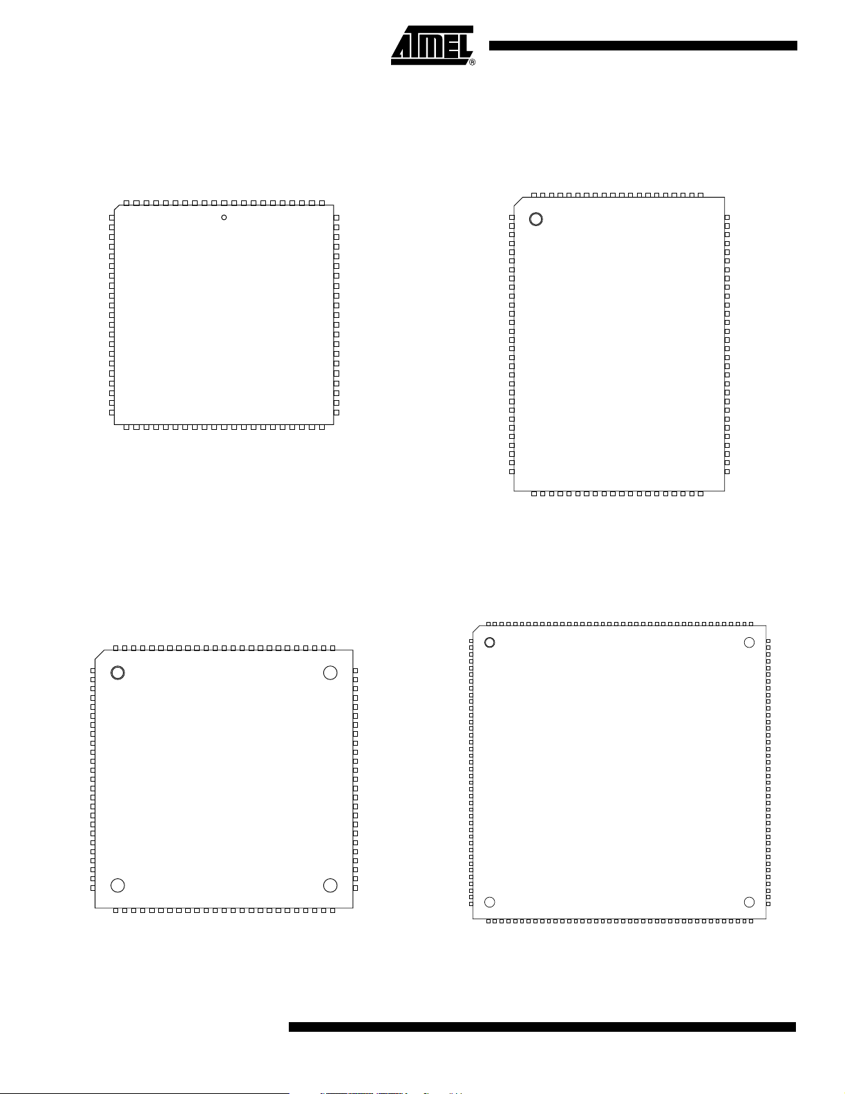
84-lead PLCC
Top View
I/O
I/O
I/O
I/O
GND
I/O
I/O
I/O
VCCINT
INPUT/OE2/GCLK2
INPUT/GCLR
INPUT/OE1
INPUT/GCLK1
987654321
11
10
12
13
14
15
I/O
16
I/O
17
I/O
18
I/O
19
20
I/O
21
I/O
22
I/O
23
24
I/O
25
I/O
26
27
I/O
28
I/O
29
I/O
30
I/O
31
I/O
32
333435363738394041424344454647484950515253
I/O
I/O
I/O
I/O
I/O
I/O
I/O
I/O
VCCIO
GND
848382818079787776
I/O
I/O
GND
I/O/PD2
VCCINT
I/O/GCLK3
I/O
I/O
I/O
I/O
GND
VCCIO
I/O
I/O
I/O
I/O
I/O
I/O
75
74
73
72
71
70
69
68
67
66
65
64
63
62
61
60
59
58
57
56
55
54
VCCIO
I/O
I/O
GND
I/O/TDO
I/O
I/O
I/O
I/O
VCCIO
I/O
I/O
I/O
I/O/TCK
I/O
I/O
GND
I/O
I/O
I/O
I/O
I/O
I/O/PD1
VCCIO
I/O/TDI
GND
I/O/TMS
VCCIO
GND
100-lead PQFP
Top View
I/O
I/O
I/O
GND
I/O
I/O
I/O
VCCINT
INPUT/OE2/GCLK2
INPUT/GCLR
99989796959493929190898887868584838281
100
1
I/O
2
I/O
3
4
I/O
5
6
7
I/O
8
I/O
9
I/O
10
I/O
11
I/O
12
I/O
13
14
I/O
15
I/O
16
I/O
17
18
I/O
19
I/O
20
21
I/O
22
I/O
23
I/O
24
I/O
25
I/O
26
I/O
27
I/O
28
29
I/O
30
I/O
31323334353637383940414243444546474849
I/O
I/O
I/O
I/O
I/O
I/O
I/O
I/O
GND
VCCIO
INPUT/OE1
INPUT/GCLK1
GND
I/O
I/O/PD2
VCCINT
I/O/GCLK3
I/O
I/O
I/O
I/O
GND
VCCIO
I/O
I/O
I/O
I/O
80
I/O
79
I/O
78
I/O
77
I/O
76
GND
75
I/O/TDO
74
I/O
73
I/O
72
I/O
71
I/O
70
I/O
69
I/O
68
VCCIO
67
I/O
66
I/O
65
I/O
64
I/O/TCK
63
I/O
62
I/O
61
GND
60
I/O
59
I/O
58
I/O
57
I/O
56
I/O
55
I/O
54
I/O
53
VCCIO
52
I/O
51
I/O
50
I/O
I/O
I/O
I/O/PD1
VCCIO
I/O/TDI
GND
I/O/TMS
VCCIO
100-lead TQFP
Top View
I/O
I/O
I/O
I/O
I/O
GND
I/O
I/O
I/O
VCCINT
INPUT/OE2/GCLK2
INPUT/GCLR
INPUT/OE1
INPUT/GCLK1
GND
I/O/GCLK3
9998979695949392919089888786858483828180797877
100
1
2
I/O
3
4
5
I/O
6
I/O
7
I/O
8
I/O
9
I/O
10
I/O
11
12
I/O
13
I/O
14
I/O
15
16
I/O
17
I/O
18
19
I/O
20
I/O
21
I/O
22
I/O
23
I/O
24
I/O
25
I/O
26272829303132333435363738394041424344454647484950
I/O
I/O
I/O
I/O
I/O
I/O
I/O
I/O
I/O
I/O
GND
VCCIO
GND
I/O
VCCINT
I/O/PD2
160-lead PQFP
Top View
I/O
I/O/PD2
I/O
N/C
N/C
N/C
N/C
I/O
I/O
I/O
I/O
I/O
GND
I/O
I/O
I/O
I/O
VCCINT
INPUT/OE2/GCLK2
INPUT/GCLR
INPUT/OE1
INPUT/GCLK1
GND
I/O/GCLK3
I/O
I/O
I/O
VCCIO
I/O
I/O
I/O
I/O
I/O
N/C
N/C
N/C
N/C
I/O
I/O
I/O
160
159
158
157
156
155
154
153
152
151
150
149
148
147
146
145
144
143
142
141
140
139
138
137
136
135
134
133
132
131
130
129
128
127
126
125
124
123
122
121
120
1
I/O
I/O
VCCIO
I/O
I/O
I/O
I/O
I/O
I/O
76
75
I/O
74
GND
73
I/O/TDO
72
I/O
71
I/O
70
I/O
69
I/O
68
I/O
67
I/O
66
VCCIO
65
I/O
64
I/O
63
I/O
62
I/O/TCK
61
I/O
60
I/O
59
GND
58
I/O
57
I/O
56
I/O
55
I/O
54
I/O
53
I/O
52
I/O
51
VCCIO
I/O
I/O
I/O
I/O
I/O
I/O
I/O
GND
I/O
N/C
2
N/C
3
N/C
4
N/C
5
N/C
6
N/C
7
N/C
8
VCCIO
9
I/O/TDI
10
I/O
11
I/O
12
I/O
13
I/O
14
I/O
15
I/O
16
I/O
17
GND
18
I/O
19
I/O
20
I/O
21
I/O
22
I/O/TMS
23
I/O
24
I/O
25
I/O
26
VCCIO
27
I/O
28
I/O
29
I/O
30
I/O
31
I/O
32
I/O
33
I/O
34
N/C
35
N/C
36
N/C
37
N/C
38
N/C
39
N/C
40
N/C
414243444546474849505152535455565758596061626364656667686970717273747576777879
I/O
I/O
I/O
I/O
I/O
I/O
I/O
I/O
I/O
I/O
I/O
I/O
I/O
I/O
I/O
N/C
N/C
N/C
N/C
GND
VCCIO
GND
VCCINT
I/O/PD1
I/O
GND
I/O
I/O
I/O
I/O
I/O
I/O
I/O
N/C
N/C
N/C
N/C
119
N/C
118
N/C
117
N/C
116
N/C
115
N/C
114
N/C
113
GND
112
I/O/TDO
111
I/O
110
I/O
109
I/O
108
I/O
107
I/O
106
I/O
105
I/O
104
VCCIO
103
I/O
102
I/O
101
I/O
100
I/O
99
I/O/TCK
98
I/O
97
I/O
96
I/O
95
GND
94
I/O
93
I/O
92
I/O
91
I/O
90
I/O
89
I/O
88
I/O
87
N/C
86
N/C
85
N/C
84
N/C
83
N/C
82
N/C
81
N/C
80
I/O
I/O
N/C
VCCIO
2
ATF1508AS(L)
0784O–PLD–09/02
Page 3
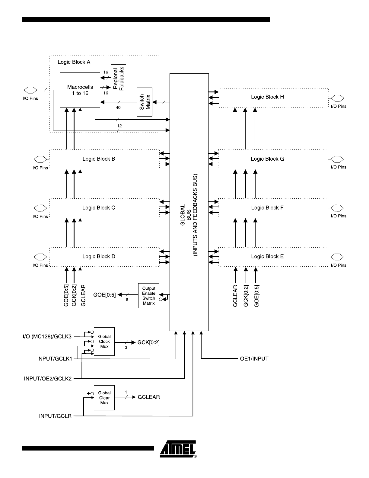
Block Diagram
8to12
ATF1508AS(L)
16
0784O–PLD–09/02
3
Page 4

Description The ATF1508AS is a high-performance, high-density complex programmable logic device
(CPLD) that utilizes Atmel’s proven electrically-erasable technology. With 128 logic macrocells
and up to 100 inputs, it easily integrates logic from several TTL, SSI, MSI, LSI and classic
PLDs. The ATF1508AS’s enhanced routing switch matrices increase usable gate count and
increase odds of successful pin-locked design modifications.
The ATF1508AS has up to 96 bi-directional I/O pins and four dedicated input pins, depending
on the type of device package selected. Each dedicated pin can also serve as a global control
signal, register clock, register reset or output enable. Each of these control signals can be
selected for use individually within each macrocell.
Each of the 128 macrocells generates a buried feedback that goes to the global bus. Each
input and I/O pin also feeds into the global bus. The switch matrix in each logic block then
selects 40 individual signals from the global bus. Each macrocell also generates a foldback
logic term that goes to a regional bus. Cascade logic between macrocells in the ATF1508AS
allows fast, efficient generation of complex logic functions. The ATF1508AS contains eight
suchlogicchains,eachcapableofcreatingsumtermlogicwithafan-inofupto40product
terms.
The ATF1508AS macrocell, shown in Figure 1, is flexible enough to support highly-complex
logic functions operating at high speed. The macrocell consists of five sections: product terms
and product term select multiplexer; OR/XOR/CASCADE logic, a flip-flop, output select and
enable, and logic array inputs.
Unused macrocells are automatically disabled by the compiler to decrease power consumption. A security fuse, when programmed, protects the contents of the ATF1508AS. Two bytes
(16 bits) of User Signature are accessible to the user for purposes such as storing project
name, part number, revision or date. The User Signature is accessible regardless of the state
of the security fuse.
Product Terms and Select Mux
OR/XOR/ CASCADE Logic
The ATF1508AS device is an in-system programmable (ISP) device. It uses the industry-standard 4-pin JTAG interface (IEEE Std. 1149.1), and is fully compliant with JTAG’s Boundaryscan Description Language (BSDL). ISP allows the device to be programmed without removing it from the printed circuit board. In addition to simplifying the manufacturing flow, ISP also
allows design modifications to be made in the field via software.
Each ATF1508AS macrocell has five product terms. Each product term receives as its inputs
all signals from both the global bus and regional bus.
The product term select multiplexer (PTMUX) allocates the five product terms as needed to
the macrocell logic gates and control signals. The PTMUX programming is determined by the
design compiler, which selects the optimum macrocell configuration.
The ATF1508AS’s logic structure is designed to efficiently support all types of logic. Within a
single macrocell, all the product terms can be routed to the OR gate, creating a 5-input
AND/OR sum term. With the addition of the CASIN from neighboring macrocells, this can be
expanded to as many as 40 product terms with a little small additional delay.
The macrocell’s XOR gate allows efficient implementation of compare and arithmetic functions. One input to the XOR comes from the OR sum term. The other XOR input can be a
product term or a fixed high- or low-level. For combinatorial outputs, the fixed level input
allows polarity selection. For registered functions, the fixed levels allow DeMorgan minimization of product terms. The XOR gate is also used to emulate T- and JK-type flip-flops.
4
ATF1508AS(L)
0784O–PLD–09/02
Page 5

ATF1508AS(L)
Flip-flop The ATF1508AS’s flip-flop has very flexible data and control functions. The data input can
come from either the XOR gate, from a separate product term or directly from the I/O pin.
Selecting the separate product term allows creation of a buried registered feedback within a
combinatorial output macrocell. (This feature is automatically implemented by the fitter software). In addition to D, T, JK and SR operation, the flip-flop can also be configured as a flowthrough latch. In this mode, data passes through when the clock is high and is latched when
the clock is low.
The clock itself can be either the Global CLK Signal (GCK) or an individual product term. The
flip-flop changes state on the clock’s rising edge. When the GCK signal is used as the clock,
one of the macrocell product terms can be selected as a clock enable. When the clock enable
function is active and the enable signal (product term) is low, all clock edges are ignored. The
flip-flop’s asynchronous reset signal (AR) can be either the Global Clear (GCLEAR), a product
term, or always off. AR can also be a logic OR of GCLEAR with a product term. The asynchronous preset (AP) can be a product term or always off.
Extra Feedback The ATF15xxSE Family macrocell output can be selected as registered or combinatorial. The
extra buried feedback signal can be either combinatorial or a registered signal regardless of
whether the output is combinatorial or registered. (This enhancement function is automatically
implemented by the fitter software.) Feedback of a buried combinatorial output allows the creation of a second latch within a macrocell.
I/O Control The output enable multiplexer (MOE) controls the output enable signal. Each I/O can be indi-
vidually configured as an input, output or for bi-directional operation. The output enable for
each macrocell can be selected from the true or compliment of the two output enable pins, a
subset of the I/O pins, or a subset of the I/O macrocells. This selection is automatically done
by the fitter software when the I/O is configured as an input, all macrocell resources are still
available, including the buried feedback, expander and cascade logic.
Global Bus/Switch Matrix
The global bus contains all input and I/O pin signals as well as the buried feedback signal from
all 128 macrocells. The switch matrix in each logic block receives as its inputs all signals from
the global bus. Under software control, up to 40 of these signals can be selected as inputs to
the logic block.
Foldback Bus Each macrocell also generates a foldback product term. This signal goes to the regional bus
and is available to 16 macrocells. The foldback is an inverse polarity of one of the macrocell’s
product terms. The 16 foldback terms in each region allows generation of high fan-in sum
terms (up to 21 product terms) with a little additional delay.
3.3V or 5.0V I/O Operation
Open-collector Output Option
The ATF1508AS device has two sets of VCCpins viz, V
always be connected to a 5.0V power supply. V
patible” with both 3.3V and 5.0V inputs. V
connected for 3.3/5.0V power supply.
This option enables the device output to provide control signals such as an interrupt that can
be asserted by any of the several devices.
CCIO
pins are for input buffers and are “com-
CCINT
pins are for I/O output drives and can be
CCINT
and V
CCIO.VCCINT
pins must
0784O–PLD–09/02
5
Page 6
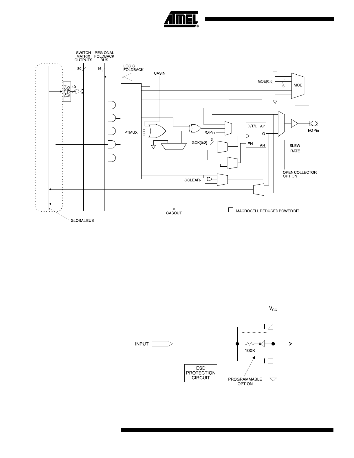
Figure 1. ATF1508AS Macrocell
Programmable Pin-keeper Option for Inputs and I/Os
Input Diagram
The ATF1508AS offers the option of programming all input and I/O pins so that “pin-keeper”
circuits can be utilized. When any pin is driven high or low and then subsequently left floating,
it will stay at that previous high- or low-level. This circuitry prevents unused input and I/O lines
from floating to intermediate voltage levels, which causes unnecessary power consumption
and system noise. The keeper circuits eliminate the need for external pull-up resistors and
eliminate their DC power consumption.
6
ATF1508AS(L)
0784O–PLD–09/02
Page 7
ATF1508AS(L)
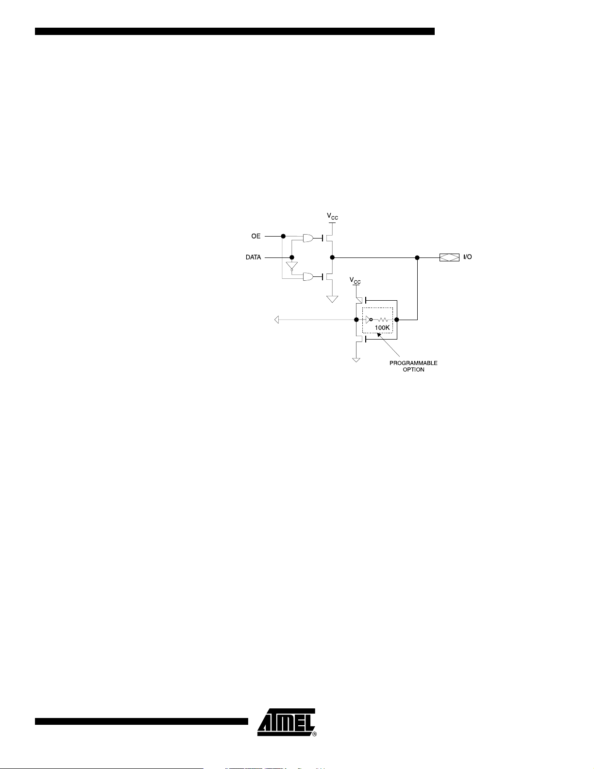
Speed/Power Management
I/O Diagram
The ATF1508AS has several built-in speed and power management features. The
ATF1508AS contains circuitry that automatically puts the device into a low-power stand-by
mode when no logic transitions are occurring. This not only reduces power consumption during inactive periods, but also provides proportional power-savings for most applications
running at system speeds below 5 MHz.
To further reduce power, each ATF1508AS macrocell has a Reduced-power bit feature. This
feature allows individual macrocells to be configured for maximum power savings. This feature
may be selected as a design option.
All ATF1508 also have an optional power-down mode. In this mode, current drops to below 10
mA. When the power-down option is selected, either PD1 or PD2 pins (or both) can be used to
power down the part. The power-down option is selected in the design source file. When
enabled, the device goes into power-down when either PD1 or PD2 is high. In the power-down
mode, all internal logic signals are latched and held, as are any enabled outputs.
All pin transitions are ignored until the PD pin is brought low. When the power-down feature is
enabled, the PD1 or PD2 pin cannot be used as a logic input or output. However, the pin’s
macrocell may still be used to generate buried foldback and cascade logic signals.
All power-down AC characteristic parameters are computed from external input or I/O pins,
with Reduced-power Bit turned on. For macrocells in reduced-power mode (Reduced-power
bit turned on), the reduced-power adder, tRPA, must be added to the AC parameters, which
include the data paths t
Each output also has individual slew rate control. This may be used to reduce system noise by
slowing down outputs that do not need to operate at maximum speed. Outputs default to slow
switching, and may be specified as fast switching in the design file.
LAD,tLAC,tIC,tACL,tACH
and t
SEXP
.
0784O–PLD–09/02
7
Page 8

Design
Software
ATF1508AS designs are supported by several third-party tools. Automated fitters allow logic
synthesis using a variety of high level description languages and formats.
Support
Power-up Reset The ATF1508AS is designed with a power-up reset, a feature critical for state machine initial-
ization. At a point delayed slightly from V
the state of each output will depend on the polarity of its buffer. However, due to the asynchronous nature of reset and uncertainty of how V
conditions are required:
1. The V
2. After reset occurs, all input and feedback setup times must be met before driving the
clock pin high, and,
3. The clock must remain stable during T
The ATF1508AS has two options for the hysteresis about the reset level, V
Large. During the fitting process users may configure the device with the Power-up Reset hysteresis set to Large or Small. Atmel POF2JED users may select the Large option by including
the flag “-power_reset” on the command line after “filename.POF”. To allow the registers to be
properly reinitialized with the Large hysteresis option selected, the following condition is
added:
4. If V
When the Large hysteresis option is active, I
well.
rise must be monotonic,
CC
falls below 2.0V, it must shut off completely before the device is turned on again.
CC
crossing V
CC
actually rises in the system, the following
CC
.
D
is reduced by several hundred microamps as
CC
, all registers will be initialized, and
RST
RST
, Small and
Security Fuse Usage
A single fuse is provided to prevent unauthorized copying of the ATF1508AS fuse patterns.
Once programmed, fuse verify is inhibited. However, User Signature and device ID remains
accessible.
Programming ATF1508AS devices are in-system programmable (ISP) devices utilizing the 4-pin JTAG pro-
tocol. This capability eliminates package handling normally required for programming and
facilitates rapid design iterations and field changes.
Atmel provides ISP hardware and software to allow programming of the ATF1508AS via the
PC. ISP is performed by using either a download cable or a comparable board tester or a simple microprocessor interface.
To allow ISP programming support by the Automated Test Equipment (ATE) vendors, Serial
Vector Format (SVF) files can be created by the Atmel ISP Software. Conversion to other ATE
tester format beside SVF is also possible
ATF1508AS devices can also be programmed using standard third-party programmers. With
third-party programmer, the JTAG ISP port can be disabled thereby allowing four additional
I/Opinstobeusedforlogic.
Contact your local Atmel representatives or Atmel PLD applications for details.
8
ATF1508AS(L)
0784O–PLD–09/02
Page 9

ATF1508AS(L)
ISP Programming Protection
JTAG-BST Overview
The ATF1508AS has a special feature that locks the device and prevents the inputs and I/O
from driving if the programming process is interrupted for any reason. The inputs and I/O
default to high-Z state during such a condition. In addition the pin-keeper option preserves the
former state during device programming.
All ATF1508AS devices are initially shipped in the erased state thereby making them ready to
use for ISP.
Note: For more information refer to the “Designing for In-System Programmability with Atmel CPLDs”
application note.
The JTAG boundary-scan testing is controlled by the Test Access Port (TAP) controller in the
ATF1508AS. The boundary-scan technique involves the inclusion of a shift-register stage
(contained in a boundary-scan cell) adjacent to each component so that signals at component
boundaries can be controlled and observed using scan testing principles. Each input pin and
I/O pin has its own boundary-scan cell (BSC) in order to support boundary-scan testing. The
ATF1508AS does not currently include a Test Reset (TRST) input pin because the TAP controller is automatically reset at power-up. The six JTAG BST modes supported include:
SAMPLE/PRELOAD, EXTEST, BYPASS and IDCODE. BST on the ATF1508AS is implemented using the Boundary-scan Definition Language (BSDL) described in the JTAG
specification (IEEE Standard 1149.1). Any third-party tool that supports the BSDL format can
be used to perform BST on the ATF1508AS.
The ATF1508AS also has the option of using four JTAG-standard I/O pins for In-System programming (ISP). The ATF1508AS is programmable through the four JTAG pins using
programming compatible with the IEEE JTAG Standard 1149.1. Programming is performed by
using 5V TTL-level programming signals from the JTAG ISP interface. The JTAG feature is a
programmable option. If JTAG (BST or ISP) is not needed, then the four JTAG control pins are
available as I/O pins.
JTAG Boundary-scan Cell (BSC) Testing
The ATF1508AS contains up to 96 I/O pins and four input pins, depending on the device type
and package type selected. Each input pin and I/O pin has its own boundary-scan cell (BSC)
in order to support boundary-scan testing as described in detail by IEEE Standard 1149.1. A
typical BSC consists of three capture registers or scan registers and up to two update registers. There are two types of BSCs, one for input or I/O pin, and one for the macrocells. The
BSCs in the device are chained together through the (BST) capture registers. Input to the capture register chain is fed in from the TDI pin while the output is directed to the TDO pin.
Capture registers are used to capture active device data signals, to shift data in and out of the
device and to load data into the update registers. Control signals are generated internally by
the JTAG TAP controller. The BSC configuration for the input and I/O pins and macrocells are
shown below.
0784O–PLD–09/02
9
Page 10

BSC
Configuration
Pins and
Macrocells
(Except JTAG
TAP Pin s
)
BSC Configuration for Macrocell
Note: The ATF1508AS has a pull-up option on TMS and TDI pins. This feature is selected as a design
option.
TDO
OEJ
OUTJ
0
DQ
1
0
DQ
1
DQ
DQ
0
1
0
1
Pin
Boundary Scan Definition Language (BSDL) Models for the ATF1508
10
ATF1508AS(L)
Capture
DR
TDI
Shift
Macrocell BSC
Update
DR
Mode
Clock
These are now available in all package types via the Atmel Web Site. These models can be
used for Boundary-scan Test Operation in the ATF1508AS and have been scheduled to conform to the IEEE 1149.1 standard.
0784O–PLD–09/02
Page 11

ATF1508AS(L)
PCI Compliance The ATF1508AS also supports the growing need in the industry to support the new Peripheral
Component Interconnect (PCI) interface standard in PCI-based designs and specifications.
The PCI interface calls for high current drivers, which are much larger than the traditional TTL
drivers.
PCI Voltage-tocurrent Curves
for +5V
Signaling in
Pull-up Mode
PCI Voltage-tocurrent Curves
for +5V
Signaling in
Pull-down Mode
VCC
2.4
1.4
VCC
2.2
Voltage
-2
AC drive
Voltage
DC
drive point
AC drive
point
point
Pull Up
-44
Pull Down
Current (mA)
Test Point
-178
0784O–PLD–09/02
0.55
DC
drive point
3,6
95
Test Point
Current (mA)
380
11
Page 12

PCI DC Characteristics
Symbol Parameter Conditions Min Max Units
V
V
V
I
IH
I
IL
V
V
C
C
C
L
CC
IH
IL
OH
OL
IN
CLK
IDSEL
PIN
Supply Voltage 4.75 5.25 V
Input High Voltage 2.0 VCC+0.5 V
Input Low Voltage -0.5 0.8 V
Input High Leakage Current
Input Low Leakage Current
Output High Voltage I
Output Low Voltage I
(1)
(1)
VIN=2.7V 70 µA
VIN= 0.5V -70 µA
=-2mA 2.4 V
OUT
=3mA,6mA 0.55 V
OUT
Input Pin Capacitance 10 pF
CLK Pin Capacitance 12 pF
IDSEL Pin Capacitance 8pF
Pin Inductance 20 nH
Note: 1. Leakage current is without pin-keeper off.
PCI AC Characteristics
Symbol Parameter Conditions Min Max Units
I
OH(AC)
Switching 0 < V
Current High 1.4 < V
(Test High) V
I
OL(AC)
Switching V
Current Low 2.2 > V
(Test Point) V
I
CL
SLEW
SLEW
R
F
Low Clamp Current -5 < VIN≤ -1 -25+(VIN+1)/0.015 mA
Output Rise Slew Rate 0.4V to 2.4V load 0.5 3.0 V/ns
Output Fall Slew Rate 2.4V to 0.4V load 0.5 3.0 V/ns
Notes: 1. Equation A: I
2. Equation B: I
=11.9(V
OH
= 78.5 * V
OL
- 5.25) * (V
OUT
*(4.4-V
OUT
3.1 < V
0.1 > V
OUT
)for0V<V
OUT
≤ 1.4 -44 mA
OUT
< 2.4 -44+(V
OUT
OUT<VCC
=3.1V -142 µA
OUT
> 2.2V 95 mA
OUT
>0 V
OUT
> 0 Equation B
OUT
= 0.71 206 mA
OUT
+ 2.45) for VCC>V
< 0.71V.
OUT
OUT
>3.1V.
- 1.4)/0.024 mA
OUT
Equation A
/0.023 mA
OUT
(1)
(2)
mA
mA
12
ATF1508AS(L)
0784O–PLD–09/02
Page 13

ATF1508AS(L)
Power-down Mode
The ATF1508AS includes two pins for optional pin-controlled power-down feature. When this
mode is enabled, the PD pin acts as the power-down pin. When the PD1 and PD2 pin is high,
the device supply current is reduced to less than 10 mA. During power-down, all output data
and internal logic states are latched and held. Therefore, all registered and combinatorial output data remain valid. Any outputs that were in a high-Z state at the onset will remain at highZ. During power-down, all input signals except the power-down pin are blocked. Input and I/O
hold latches remain active to ensure that pins do not float to indeterminate levels, further
reducing system power. The power-down pin feature is enabled in the logic design file.
Designs using either power-down pin may not use the PD pin logic array input. However, buried logic resources in this macrocell may still be used.
Power-down AC Characteristics
Symbol Parameter
t
IVDH
t
GVDH
t
CVDH
t
DHIX
t
DHGX
t
DHCX
t
DLIV
t
DLGV
t
DLCV
t
DLOV
Notes: 1. For slow slew outputs, add t
Valid I, I/O before PD High 7 10 15 20 25 ns
Valid OE
Valid Clock
(2)
before PD High 7 10 15 20 25 ns
(2)
before PD High 7 10 15 20 25 ns
I, I/O Don’t Care after PD High 12 15 25 30 35 ns
(2)
OE
Don’t Care after PD High 12 15 25 30 35 ns
(2)
Clock
Don’t Care after PD High 12 15 25 30 35 ns
PD Low to Valid I, I/O 1 1 1 1 1 µs
PD Low to Valid OE (Pin or Term) 1 1 1 1 1 µs
PD Low to Valid Clock (Pin or Term) 1 1 1 1 1 µs
PD Low to Valid Output 1 1 1 1 1 µs
.
SSO
2. Pin or product term.
(1)(2)
-7 -10 -15 -20 -25
UnitsMin Max Min Max Min Max Min Max Min Max
Absolute Maximum Ratings*
Temperature Under Bias .................................. -40°C to +85°C
Storage Temperature ..................................... -65°C to +150°C
Voltage on Any Pin with
Respect to Ground .........................................-2.0V to +7.0V
Voltage on Input Pins
with Respect to Ground
During Programming.....................................-2.0V to +14.0V
Programming Voltage with
Respect to Ground .......................................-2.0V to +14.0V
0784O–PLD–09/02
*NOTICE: Stresses beyond those listed under “Absolute
Maximum Ratings” may cause permanent damage to the device. This is a stress rating only and
functional operation of the device at these or any
(1)
other conditions beyond those indicated in the
operational sections of this specification is not
implied. Exposure to absolute maximum rating
conditions for extended periods may affect device
(1)
Note: 1. Minimum voltage is -0.6V DC, which may under-
reliability.
shoot to -2.0V for pulses of less than 20 ns.
(1)
which may overshoot to 7.0V for pulses of less
Maximum output pin voltage is V
+ 0.75V DC,
CC
than 20 ns.
13
Page 14

DC and AC Operating Conditions
Commercial Industrial
Operating Temperature (Ambient) 0°C - 70°C -40°C - 85°C
V
or V
CCINT
V
(3.3V) Power Supply 2.7V - 3.6V 2.7V - 3.6V
CCIO
(5V) Power Supply 5V ± 5% 5V ± 10%
CCIO
DC Characteristics
(1)
Symbol Parameter Condition Min Typ Max Units
I
IL
Input or I/O Low
VIN=V
CC
-2 -10 µA
Leakage Current
I
IH
Input or I/O High
210µA
Leakage Current
I
OZ
Tri-state Output
VO=VCCor GND -40 40 µA
Off-state Current
I
CC1
Power Supply
Current, Standby
VCC=Max
V
=0,V
IN
Std Mode Com. 160 mA
CC
Ind. 180 mA
“L” Mode Com. 10 µA
Ind. 10 µA
I
I
V
V
V
V
V
V
CC2
CC3
CCIO
CCIO
IL
IH
OL
OH
Power Supply Current,
Power-down Mode
(2)
Reduced-power Mode
Supply Current
Supply Voltage
Supply Voltage 3.3V Device Output 3.0 3.6 V
Input Low Voltage -0.3 0.8 V
Input High Voltage 2.0 V
Output Low Voltage (TTL)
Output Low Voltage (CMOS)
Output High Voltage (TTL)
VCC=Max
V
=0,V
IN
V
=Max
CC
V
=0,V
IN
“PD” Mode 1 10 mA
CC
Std Mode Com. 65 mA
CC
Ind. 85 mA
5.0V Device Output Com. 4.75 5.25 V
Ind. 4.5 5.5 V
+0.3 V
CCIO
V
IN=VIH
V
CCIO
V
IN=VIH
VCC=MIN,IOL=0.1mA
V
IN=VIH
V
CCIO
or V
IL
=MIN,IOL=12mA
or V
IL
or V
IL
=MIN,IOH=-4.0mA
Com. 0.45 V
Ind. 0.45 V
Com. 0.2 V
Ind. 0.2 V
2.4 V
Notes: 1. Not more than one output at a time should be shorted. Duration of short circuit test should not exceed 30 sec.
2. I
refers to the current in the reduced-power mode when macrocell reduced-power is turned ON.
CC3
14
ATF1508AS(L)
0784O–PLD–09/02
Page 15

ATF1508AS(L)
Pin Capacitance
C
IN
C
I/O
Note: 1. Typical values for nominal supply voltage. This parameter is only sampled and is not 100% tested. The OGI pin (high-voltage
pin during programming) has a maximum capacitance of 12 pF.
(1)
Typ Max Units Conditions
810 pF V
810 pF V
=0V;f=1.0MHz
IN
=0V;f=1.0MHz
OUT
Timing Model
U
Input Test Waveforms and Measurement Levels
rR,tF= 1.5 ns typical
Output AC Test Loads
(3.0V)*
(703 )*
(8060 )*
Note: *Numbers in parenthesis refer to 3.0V operating conditions (preliminary).
0784O–PLD–09/02
15
Page 16

SUPPLY CURRENT VS. FREQUENCY
SUPPLY CURRENT V S. SUP PLY VOLT AGE
= 25°C, F = 0)
(T
250.0
200.0
(mA)
150.0
CC
I
100.0
STANDARD POWER
A
REDUCED POWER MODE
200.0
150.0
(mA)
100.0
CC
I
50.0
LOW-POWER ("L") VERSION
(T
STANDARD POWER
= 25°C)
A
REDUCED POWER MODE
50.0
4.50 4.75 5.00 5.25 5.50
V
(V)
CC
SUPPLY CURRENT V S. SUP PLY VOLTAGE
LOW-POWER ("L") VERSION
(T
= 25°C, F = 0)
30.0
20.0
A)
µ
µ
µ
µ
(
CC
I
10.0
0.0
4.50 4.75 5.00 5.25 5.50
A
V
(V)
CC
SUPPLY CURRENT VS. FREQUENCY
STANDARD POWER
(T
= 25°C, F = 0)
300.0
250.0
200.0
A)
µ
µ
µ
µ
(
150.0
CC
I
100.0
50.0
STANDARD POWER
0.0
0.00 2 0.00 40.00 60.00 80.00 100.00
A
REDUCED POWER MODE
FREQUENCY (MHz)
0.0
0.00 5.00 10.00 15.00 20.00
FREQUE NCY (MHz)
OUTPUT SOURCE CURRENT
VS. S UPPLY VOL TAGE (VOH = 2.4V, T
0
-10
-20
-30
IOH (mA)
-40
-50
-60
4.50 4.75 5.00 5.25 5.50
SUPP LY VOLT AGE (V)
= 25°C)
A
INPUT CLAMP CURRENT
VS. INPUT VOLTAGE (V
0
-20
-40
-60
-80
-100
INPUT CURRENT (mA)
-120
-140
-160
-1.4 -1.2 -1.0 -0 .8 -0.6 -0 .4 -0.2 0.0
INPUT VOL TAGE (V)
=5V,TA= 25°C)
CC
16
SUPPLY CURRENT VS. SUPPLY VOLTAGE
PIN-CONTROLLED POWER-DOWN MODE
(T
= 25°C, F = 0)
1100.0
A)
µ
µ
µ
µ
(
CC
I
1000.0
STANDARD POWER
900.0
800.0
700.0
4.50 4.75 5.00 5.25 5.50
A
REDUCED POWER MODE
V
(V)
CC
ATF1508AS(L)
OUTPUT SINK CURRENT
VS. SUPPLY VOLTAGE ( VOL = 0.5V, T
43
42
41
40
39
IOL (mA)
38
37
36
4.50 4.75 5 .00 5.25 5.50
SUPPLY VOLTAGE (V)
= 25°C)
A
0784O–PLD–09/02
Page 17

ATF1508AS(L)
OUTPUT SOURCE CURRENT
VS. SUPPLY V OLTAGE ( V
-10
-30
-50
IOH (mA)
-70
-90
-110
0.0 0.5 1.0 1.5 2.0 2.5 3.0 3.5 4.0 4.5 5.0
OUTPU T VOLTA GE (V)
=5V,TA= 25°C)
CC
INPUT CURRENT
40
30
A)
µ
µ
µ
µ
20
10
0
-10
INPUT CURRENT (
-20
-30
VS. INPUT VOLTAGE (V
0.00.51.01.52.02.53.03.54.04.55.0
INPU T VOLTA GE (V)
=5V,TA= 25°C)
CC
NORMALIZED TCO
1.20
1.10
1.00
NORMALIZ ED TPD
0.90
0.80
4.50 4.75 5.00 5.25 5.50
VS. SUPPLY VOLTAGE ( T
SUPPLY VOLTAGE (V)
= 25°C)
A
NORMALIZED TSU
1.20
1.10
1.00
NORMALIZ ED TSU
0.90
0.80
4.50 4.75 5.00 5.25 5.50
VS. SUPPLY VOLTAGE ( T
SUPPLYVOLTAGE (V)
= 25°C)
A
OUTPUT SINK CURRENT
140
120
100
IOL (mA)
VS. OUTPUT VOLTAGE (V
80
60
40
20
0
0.0 0.5 1.0 1.5 2.0 2 .5 3.0 3.5 4.0 4.5 5.0
OUTPUT VOLTAGE(V)
=5V,TA= 25°C)
CC
NORMALIZED TPD
1.20
VS. SUPPLY VOLTAGE (T
1.10
1.00
NORMALIZ ED TPD
0.90
0.80
4.50 4.75 5.00 5.25 5.50
SUPP LY VOLTAGE (V)
= 25°C)
A
NORMALIZED TPD
1.20
1.10
1.00
NORMALIZ ED TPD
0.90
0.80
-40 0 25 75
VS. TEMPERATURE (V
TEMPERATURE (C)
CC
=5.0V)
NORMALIZED TCO
1.20
1.10
1.00
NORMALIZ ED TCO
0.90
0.80
-40 0 25 75
VS. TEMPERATURE (V
TEMPERATURE (C)
CC
=5.0V)
0784O–PLD–09/02
17
Page 18

NORMALIZED TSU
1.20
1.10
1.00
NORMALIZ ED TSU
0.90
0.80
-40 0 25 75
VS. TEMPERATURE (V
TEMPERATURE (C)
CC
=5.0V)
18
ATF1508AS(L)
0784O–PLD–09/02
Page 19

ATF1508AS(L)
AC Characteristics
Symbol Parameter
t
PD1
t
PD2
t
SU
t
H
t
FSU
t
FH
t
COP
t
CH
t
CL
t
ASU
t
AH
t
ACOP
t
ACH
t
ACL
t
CNT
f
CNT
Input or Feedback to
Non-registered Output
I/O Input or Feedback to
Non-registered Feedback
Global Clock Setup Time 6 7 11 16 20 ns
Global Clock Hold Time 0 0 0 0 0 ns
Global Clock Setup Time of
Fast Input
Global Clock Hold Time of
Fast Input
Global Clock to Output Delay 4.5 5 8 10 13 ns
Global Clock High Time 3 4 5 6 7 ns
Global Clock Low Time 3 4 5 6 7 ns
Array Clock Setup Time 3 3 4 4 5 ns
Array Clock Hold Time 2 3 4 5 6 ns
Array Clock Output Delay 7.5 10 15 20 25 ns
Array Clock High Time 3 4 6 8 10 ns
Array Clock Low Time 3 4 6 8 10 ns
Minimum Clock Global Period 8 10 13 17 22 ns
Maximum Internal Global
Clock Frequency
(1)
-7 -10 -15 -20 -25
UnitsMin Max Min Max Min Max Min Max Min Max
7.5 10 3 15 20 25 ns
793121620ns
33333ns
0.5 0.5 1.0 1.5 2 MHz
125 100 76.9 66 50 MHz
t
ACNT
f
ACNT
f
MAX
t
IN
t
IO
t
FIN
t
SEXP
t
PEXP
t
LAD
t
LAC
t
IOE
t
OD1
0784O–PLD–09/02
Minimum Array Clock Period 8 10 13 17 22 ns
Maximum Internal Array
125 100 76.9 66 50 MHz
Clock Frequency
Maximum Clock Frequency 166.7 125 100 41.7 33.3 MHz
Input Pad and Buffer Delay 0.5 0.5 2 2 2 ns
I/O Input Pad and Buffer Delay 0.5 0.5 2 2 2 ns
FastInputDelay 11222ns
Foldback Term Delay 4 5 8 10 12 ns
Cascade Logic Delay 0.8 0.8 1 1 1.2 ns
Logic Array Delay 3 5678ns
Logic Control Delay 3 5678ns
InternalOutputEnableDelay 22334ns
Output Buffer and Pad Delay
21.5456ns
(Slow slew rate = OFF;
V
=5V;CL=35pF)
CCIO
19
Page 20

AC Characteristics (Continued)
Symbol Parameter
(1)
-7 -10 -15 -20 -25
UnitsMin Max Min Max Min Max Min Max Min Max
t
OD2
t
OD3
t
ZX1
t
ZX2
t
ZX3
t
XZ
t
SU
t
H
t
FSU
t
FH
Output Buffer and Pad Delay
2.52.0567ns
(Slow slew rate = OFF;
V
=3.3V;CL=35pF)
CCIO
Output Buffer and Pad Delay
55.5 8 10 12ns
(Slow slew rate = ON;
V
=5Vor3.3V;CL=35pF)
CCIO
Output Buffer Enable Delay
4.0 5.0 7 9 10 ns
(Slow slew rate = OFF;
V
=5.0V;CL=35pF)
CCIO
Output Buffer Enable Delay
4.5 5.5 7 9 10 ns
(Slow slew rate = OFF;
V
=3.3V;CL=35pF)
CCIO
Output Buffer Enable Delay
9 9 10 11 12 ns
(Slow slew rate = ON;
V
= 5.0V/3.3V; CL=35pF)
CCIO
Output Buffer Disable Delay
(C
=5pF)
L
45678ns
Register Setup Time 3 2 4 5 6 ns
Register Hold Time 2 3 4 5 6 ns
Register Setup Time of Fast
33223ns
Input
Register Hold Time of Fast
0.5 0.5 2 2 2.5 ns
Input
t
RD
t
COMB
t
IC
t
EN
t
GLOB
t
PRE
t
CLR
t
UIM
t
RPA
RegisterDelay 12122ns
CombinatorialDelay 12122ns
ArrayClockDelay 35678ns
RegisterEnableTime 35678ns
GlobalControlDelay 11111ns
RegisterPresetTime 23456ns
RegisterClearTime 23456ns
SwitchMatrixDelay 11222ns
Reduced-power Adder
(2)
10 11 13 14 15 ns
Notes: 1. See ordering information for valid part numbers.
2. The t
parameter must be added to the t
RPA
LAD,tLAC,tTIC,tACL
power mode.
,andt
parameters for macrocells running in the reduced-
SEXP
20
ATF1508AS(L)
0784O–PLD–09/02
Page 21

ATF1508AS(L)
ATF1508AS Dedicated Pinouts
Dedicated Pin 84-lead J-lead 100-lead PQFP 100-lead TQFP 160-lead PQFP
INPUT/OE2/GCLK2 2 92 90 142
INPUT/GCLR 1 91 89 141
INPUT/OE1 84 90 88 140
INPUT/GCLK1 83 89 87 139
I/O /GCLK3 81 87 85 137
I/O / PD (1, 2) 12,45 3,43 1,41 63,159
I/O / TDI(JTAG) 14 6 4 9
I/O / TMS(JTAG) 23 17 15 22
I/O / TCK(JTAG) 62 64 62 99
I/O / TDO(JTAG) 71 75 73 112
GND 7,19,32,42,
47,59,72,82
VCCINT 3,43 41,93 39,91 61,143
VCCIO 13,26,38,
53,66,78
N/C – – – 1,2,3,4,5,6,7,34,35,36,
#ofSIGNALPINS 68 84 84 100
# USER I/O PINS 64 80 80 96
13,28,40,45,
61,76,88,97
5,20,36,53,68,84 3,18,34,51,66,82 8,26,55,79,104,133
11,26,38,43,
59,74,86,95
17,42,60,66,95,
113,138,148
37,38,39,40,44,45,46,
47,74,75,76,77,81,82,
83,84,85,86,87,114,
115,116,117,118,119,
120,124,125,126,127,
154,155,156,157
OE (1, 2) Global OE Pins
GCLR Global Clear Pin
GCLK (1, 2, 3) Global Clock Pins
PD (1, 2) Power-down pins
TDI, TMS, TCK, TDO JTAG pins used for boundary scan testing or in-system programming
GND Ground Pins
VCCINT VCC pins for the device (+5V - Internal)
VCCIO VCC pins for output drivers (for I/O pins) (+5V or 3.3V - I/Os)
0784O–PLD–09/02
21
Page 22

ATF1508AS I/O Pinouts
84-lead
MC PLB
1 A – 4 2 160 33 C – 27 25 41
2A––––34C––––
3
4 A – – – 158 36 C – – – 32
5 A 11 2 100 153 37 C 30 25 23 31
6 A 10 1 99 152 38 C 29 24 22 30
7A––––39C––––
8 A 9 100 98 151 40 C 28 23 21 29
9 A – 99 97 150 41 C – 22 20 28
10A––––42C––––
11 A 8 98 96 149 43 C 27 21 19 27
12 A – – – 147 44 C – – – 25
13 A 6 96 94 146 45 C 25 19 17 24
14 A 5 95 93 145 46 C 24 18 16 23
15A––––47C––––
A/
PD1
J-lead
12 3 1 159 35 C 31 26 24 33
100-lead
PQFP
100-lead
TQFP
160-lead
PQFP MC PLB
84-lead
J-lead
100-lead
PQFP
100-lead
TQFP
160-lead
PQFP
16 A 4 94 92 144 48
17 B 22 16 14 21 49 D 41 39 37 59
18B––––50D––––
19 B 21 15 13 20 51 D 40 38 36 58
20 B – – – 19 52 D – – – 57
21 B 20 14 12 18 53 D 39 37 35 56
22 B – 12 10 16 54 D – 35 33 54
23B––––55D––––
24 B 18 11 9 15 56 D 37 34 32 53
25 B 17 10 8 14 57 D 36 33 31 52
26B––––58D––––
27 B 16 9 7 13 59 D 35 32 30 51
28 B – – – 12 60 D – – – 50
29 B 15 8 6 11 61 D 34 31 29 49
30 B – 7 5 10 62 D – 30 28 48
31B––––63D––––
32
B/
TDI
14 6 4 9 64 D 33 29 27 43
C/
TMS
23 17 15 22
65 E 44 42 40 62 97 G 63 65 63 100
22
ATF1508AS(L)
0784O–PLD–09/02
Page 23

ATF1508AS I/O Pinouts (Continued)
ATF1508AS(L)
84-lead
MC PLB
66E––––98G––––
67
68 E – – – 64 100 G – – – 102
69E46444265101G656765103
70 E – 46 44 67 102 G – 69 67 105
71E––––103G––––
72E48474568104G677068106
73E49484669105G687169107
74E––––106G––––
75E50494770107G697270108
76 E – – – 71 108 G – – – 109
77E51504872109G707371110
78 E – 51 49 73 110 G – 74 72 111
79E––––111G––––
80E52525078112
81 F – 54 52 80 113 H – 77 75 121
E/
PD2
J-lead
45 43 41 63 99 G 64 66 64 101
100-lead
PQFP
100-lead
TQFP
160-lead
PQFP MC PLB
G/
TDO
84-lead
J-lead
71 75 73 112
100-lead
PQFP
100-lead
TQFP
160-lead
PQFP
82F––––114H––––
83F54555388115H 737876122
84 F – – – 89 116 H – – – 123
85F55565490117H 747977128
86F56575591118H 758078129
87F––––119H––––
88F57585692120H 768179130
89 F – 59 57 93 121 H – 82 80 131
90F––––122H––––
91F58605894123H 778381132
92 F – – – 96 124 H – – – 134
93F60626097125H 798583135
94F61636198126H 808684136
95F––––127H––––
96
F/
TCK
62 64 62 99 128
H/
GCLK3
81 87 85 137
0784O–PLD–09/02
23
Page 24

ATF1508AS Ordering Information
t
PD
(ns)
7.5 4.5 166.7 ATF1508AS-7 JC84
10 5 125 ATF1508AS-10 JC84
10 5 125 ATF1508AS-10 Jl84
15 5 100 ATF1508AS-15 JC84
15 8 100 ATF1508AS-15 JI84
t
CO1
(ns)
f
MAX
(MHz)
Ordering Code Package
ATF1508AS-7 QC100
ATF1508AS-7 AC100
ATF1508AS-7 QC160
ATF1508AS-10 QC100
ATF1508AS-10 AC100
ATF1508AS-10 QC160
ATF1508AS-10 Ql100
ATF1508AS-10 Al100
ATF1508AS-10 Ql160
ATF1508AS-15 QC100
ATF1508AS-15 AC100
ATF1508AS-15 QC160
ATF1508AS-15 QI100
ATF1508AS-15 AI100
ATF1508AS-15 QI160
84J
100Q1
100A
160Q1
84J
100Q1
100A
160Q1
84J
100Q1
100A
160Q1
84J
100Q1
100A
160Q1
84J
100Q1
100A
160Q1
Operation Range
Commercial
(0°Cto70°C)
Commercial
(0°Cto70°C)
Industrial
(-40°Cto+85°C)
Commercial
(0°Cto70°C)
Industrial
(-40°Cto+85°C)
Using “C” Product for Industrial
To use commercial product for Industrial temperature ranges, down-grade one speed grade from the “I” to the “C” device
(7 ns “C” = 10 ns “I”) and de-rate power by 30%.
Package Type
84J 84-lead, Plastic J-leaded Chip Carrier (PLCC)
100Q1 100-lead, Plastic Quad Pin Flat Package (PQFP)
100A 100-lead, Very Thin Plastic Gull Wing Quad Flat Package (TQFP)
160Q1 160-lead, Plastic Quad Pin Flat Package (PQFP)
24
ATF1508AS(L)
0784O–PLD–09/02
Page 25

ATF1508AS(L)
ATF1508ASL Ordering Information
t
PD
(ns)
20 12 83.3 ATF1508ASL-20 JC84
25 15 70 ATF1508ASL-25 JC84
25 15 70 ATF1508ASL-25 JI84
Using “C” Product for Industrial
To use commercial product for Industrial temperature ranges, down-grade one speed grade from the “I” to the “C” device
(7 ns “C” = 10 ns “I”) and de-rate power by 30%.
t
CO1
(ns)
f
MAX
(MHz)
Ordering Code Package
84J
ATF1508ASL-20 QC100
ATF1508ASL-20 AC100
ATF1508ASL-20 QC160
ATF1508ASL-25 QC100
ATF1508ASL-25 AC100
ATF1508ASL-25 QC160
ATF1508ASL-25 QI100
ATF1508ASL-25 AI100
ATF1508ASL-25 QI160
100Q1
100A
160Q1
84J
100Q1
100A
160Q1
84J
100Q1
100A
160Q1
Operation Range
Commercial
(0°Cto70°C)
Commercial
(0°Cto70°C)
Industrial
(-40°Cto+85°C)
Package Type
84J 84-lead, Plastic J-leaded Chip Carrier (PLCC)
100Q1 100-lead, Plastic Quad Pin Flat Package (PQFP)
100A 100-lead, Very Thin Plastic Gull Wing Quad Flat Package (TQFP)
160Q1 160-lead, Plastic Quad Pin Flat Package (PQFP)
0784O–PLD–09/02
25
Page 26

Package Information
84J–PLCC
1.14(0.045) X 45°
B
e
0.51(0.020)MAX
45° MAX (3X)
Notes: 1. This package conforms to JEDEC reference MS-018, Variation AF.
2. Dimensions D1 and E1 do not include mold protrusion.
Allowable protrusion is .010"(0.254 mm) per side. Dimension D1
and E1 include mold mismatch and are measured at the extreme
material condition at the upper or lower parting line.
3. Lead coplanarity is 0.004" (0.102 mm) maximum.
PIN NO. 1
IDENTIFIER
D1
D
1.14(0.045) X 45°
E1 E
0.318(0.0125)
0.191(0.0075)
NOM
D2/E2
MAX
B1
A2
A1
A
COMMON DIMENSIONS
(Unit of Measure = mm)
SYMBOL
A 4.191 – 4.572
A1 2.286 – 3.048
A2 0.508 – –
D 30.099 – 30.353
D1 29.210 – 29.413 Note 2
E 30.099 – 30.353
E1 29.210 – 29.413 Note 2
D2/E2 27.686 – 28.702
B 0.660 – 0.813
B1 0.330 – 0.533
e 1.270 TYP
MIN
NOTE
26
2325 Orchard Parkway
TITLE
R
San Jose, CA 95131
ATF1508AS(L)
84J, 84-lead, Plastic J-leaded Chip Carrier (PLCC)
DRAWING NO.
84J
0784O–PLD–09/02
10/04/01
REV.
B
Page 27

100Q1 – PQFP
ATF1508AS(L)
C
PIN1ID
PIN 1
e
B
0º~7º
E1
E
D1
D
COMMON DIMENSIONS
A
SYMBOL
L
A1
A – 3.04 3.4
A1 0.25 0.33 0.5
D 23.20 BSC
E 17.20 BSC
E1 14.00 BSC
B 0.22 – 0.40
D1 20 BSC
L 0.73 – 1.03
e 0.65 BSC
(Unit of Measure = mm)
JEDEC STANDARD MS-022, GC-1
MIN
NOM
MAX
NOTE
R
0784O–PLD–09/02
2325 Orchard Parkway
San Jose, CA 95131
TITLE
100Q1, 100-lead, 14 x 20 mm Body, 3.2 mm Footprint, 0.65 mm Pitch,
Plastic Quad Flat Package (PQFP)
09/10/2002
DRAWING NO.
100Q1
REV.
B
27
Page 28

100A – TQFP
PIN 1
B
PIN 1 IDENTIFIER
e
E1 E
D1
D
C
0˚~7˚
A1
L
Notes: 1. This package conforms to JEDEC reference MS-026, Variation AED.
2. Dimensions D1 and E1 do not include mold protrusion. Allowable
protrusion is 0.25 mm per side. Dimensions D1 and E1 are maximum
plastic body size dimensions including mold mismatch.
3. Lead coplanarity is 0.08 mm maximum.
A2 A
SYMBOL
COMMON DIMENSIONS
(Unit of Measure = mm)
MIN
A – – 1.20
A1 0.05 – 0.15
A2 0.95 1.00 1.05
D 15.75 16.00 16.25
D1 13.90 14.00 14.10 Note 2
E 15.75 16.00 16.25
E1 13.90 14.00 14.10 Note 2
B 0.17 – 0.27
C 0.09 – 0.20
L 0.45 – 0.75
e 0.50 TYP
NOM
MAX
NOTE
28
2325 Orchard Parkway
TITLE
R
San Jose, CA 95131
ATF1508AS(L)
100A, 100-lead, 14 x 14 mm Body Size, 1.0 mm Body Thickness,
0.5 mm Lead Pitch, Thin Profile Plastic Quad Flat Package (TQFP)
10/5/2001
DRAWING NO.
100A
0784O–PLD–09/02
REV.
C
Page 29

160Q1 – PQFP
ATF1508AS(L)
D1
E1
Top View
A2
A1
e
b
L1
Side View
Notes: 1. This drawing is for general information only. Refer to JEDEC Drawing
MS-022, Variation DD-1, for additional information.
2. To be determined at seating plane.
3. Regardless of the relative size of the upper and lower body sections,
dimensions D1 and E1 are determined at the largest feature of the body
exclusive of mold Flash and gate burrs, but including any mismatch
between the upper and lower sections of the molded body.
4. Dimension b does not include Dambar protrusion. The Dambar
protrusion(s) shall not cause the lead width to exceed b maximum by more
than 0.08 mm. Dambar cannot be located on the lower radius or the lead
foot.
5. A1 is defined as the distance from the seating plane to the lowest point of
the package body.
D
E
Bottom View
COMMON DIMENSIONS
(Unit of Measure = mm)
SYMBOL
A1 0.25 – 0.50 5
A2 3.20 3.40 3.60
D 31.20 BSC 2
D1 28.00 BSC 3
E 31.20 BSC 2
E1 28.00 BSC 3
e 0.65 BSC
b 0.22 – 0.40 4
L1 1.60 REF
MIN
NOM
MAX
NOTE
R
0784O–PLD–09/02
2325 Orchard Parkway
San Jose, CA 95131
TITLE
160Q1, 160-lead, 28 x 28 mm Body, 3.2 Form Opt.,
Plastic Quad Flat Pack (PQFP)
DRAWING NO.
160Q1
A
3/28/02
REV.
29
Page 30

Atmel Headquarters Atmel Operations
Corporate Headquarters
2325 Orchard Parkway
San Jose, CA 95131
TEL 1(408) 441-0311
FAX 1(408) 487-2600
Europe
Atmel Sarl
Route des Arsenaux 41
Case Postale 80
CH-1705 Fribourg
Switzerland
TEL (41) 26-426-5555
FAX (41) 26-426-5500
Asia
Room 1219
Chinachem Golden Plaza
77 Mody Road Tsimshatsui
East Kowloon
Hong Kong
TEL (852) 2721-9778
FAX (852) 2722-1369
Japan
9F, Tonetsu Shinkawa Bldg.
1-24-8 Shinkawa
Chuo-ku, Tokyo 104-0033
Japan
TEL (81) 3-3523-3551
FAX (81) 3-3523-7581
Memory
2325 Orchard Parkway
San Jose, CA 95131
TEL 1(408) 441-0311
FAX 1(408) 436-4314
Microcontrollers
2325 Orchard Parkway
San Jose, CA 95131
TEL 1(408) 441-0311
FAX 1(408) 436-4314
La Chantrerie
BP 70602
44306 Nantes Cedex 3, France
TEL (33) 2-40-18-18-18
FAX (33) 2-40-18-19-60
ASIC/ASSP/Smart Cards
Zone Industrielle
13106 Rousset Cedex, France
TEL (33) 4-42-53-60-00
FAX (33) 4-42-53-60-01
1150 East Cheyenne Mtn. Blvd.
Colorado Springs, CO 80906
TEL 1(719) 576-3300
FAX 1(719) 540-1759
Scottish Enterprise Technology Park
Maxwell Building
East Kilbride G75 0QR, Scotland
TEL (44) 1355-803-000
FAX (44) 1355-242-743
RF/Automotive
Theresienstrasse 2
Postfach 3535
74025 Heilbronn, Germany
TEL (49) 71-31-67-0
FAX (49) 71-31-67-2340
1150 East Cheyenne Mtn. Blvd.
Colorado Springs, CO 80906
TEL 1(719) 576-3300
FAX 1(719) 540-1759
Biometrics/Imaging/Hi-Rel MPU/
High Speed Converters/RF Datacom
Avenue de Rochepleine
BP 123
38521 Saint-Egreve Cedex, France
TEL (33) 4-76-58-30-00
FAX (33) 4-76-58-34-80
e-mail
literature@atmel.com
Web Site
http://www.atmel.com
© Atmel Corporation 2002.
Atmel Corporation makes no warranty for the use of its products, other than those expressly contained in the Company’s standard warranty
which is detailed in Atmel’s Terms and Conditions located on the Company’s web site. The Company assumes no responsibility for any errors
which may appear in this document, reserves the right to change devices or specifications detailed herein at any time without notice, and does
not make any commitment to update the information contained herein. No licenses to patents or other intellectual property of Atmel are granted
by the Company in connection with the sale of Atmel products, expressly or by implication. Atmel’s products are not authorized for use as critical
components in life support devices or systems.
AT ME L®is the registered trademark of Atmel.
Other terms and product names may be the trademarks of others.
Printed on recycled paper.
0784O–PLD–09/02 xM
 Loading...