

Page 1

Features
• High-density, High-performance, Electrically-erasable Complex
ProgrammableLogic D evice
– 3.0 to 3.6V Operating Range
– 64 Macrocells
– 5 Product Terms per Macrocell, Expandable up to 40 per Macrocell
– 44, 68, 84, 100 Pins
–15nsMaximumPin-to-pinDelay
– Registered Operation up to 77 MHz
– Enhanced Routing Resources
• In-System Programmability (ISP) via JTAG
• Flexible Logic Macrocell
– D/T/Latch Configurable Flip-flops
– Global and Individual Register Control Signals
– Global and Individual Output Enable
– Programmable Out put Slew Rate
– Programmable Out put Open-collector Option
– Maximum Logic Utilization by Burying a Register with a COM Output
• Advanced Power Management Features
– Automatic 5 µA Standby for “L” Version
– Pin-control led 100 µA Standby Mode (Typical)
– Programmable Pin-keeper Circuits on Inputs and I/Os
– Reduced-power Feature per Macrocell
• Avai lable in Commercial and Industrial Temperature Ranges
• Avai lable in 44-, 68-, and 84-lead PLCC; 44- and 100-lead TQFP; and 100-lead PQFP
• Advanced EE Technology
– 100% Tested
– Completely Reprogrammable
– 10,000 Program/Erase Cycles
– 20 Year Data Retention
– 2000V ESD Protection
– 200 mA Latch-up Immunity
• JTAG Boundary-scan Testing to IEEE Std. 1149.1-1990 and 1149.1a-1993 Supported
• PCI-compliant
• Security Fuse Feature
Low-voltage,
Complex
Programmable
Logic Device
ATF1504ASV
ATF1504ASVL
Enhanced Features
• ImprovedConnectivity (Additional Feedback Routing, Alternate Input Routing)
• Output Enable Product Terms
• Transparent-latch Mode
• Combinatorial Output wi th Registered Feedback within Any Macrocell
• Three Global Clock Pins
• ITD (Input Transition Detection) Circuits on Global Clocks, Inputs and I/O
• Fast Registered I nput from Product Term
• Programmable“Pin-keeper” Option
• V
Power-up Reset Option
CC
• Pull-up Option on JTAG Pins TMS and TDI
• Advanced Power Management Features
– Edge-controlled Power-down “L”
– Individual Macrocell Power Option
– Disable ITD on Global Clocks, Inputs and I/O
Rev. 1409H–PLD–09/02
1
Page 2
I/O/TDI
GND
PD1/I/O
TMS/I/O
VCC
44-lead TQFP
Top View
I/O
I/O
I/O
VCC
GCLK2/OE2/I
GCLR/I
I/OE1
GCLK1/I
GND
GCLK3/I/O
I/O
4443424140393837363534
33
1
2
I/O
3
I/O
4
5
6
I/O
7
8
I/O
9
10
I/O
11
I/O
1213141516171819202122
I/O
I/O
I/O
I/O
I/O
I/O
GND
VCC
I/O
PD2/I/O
I/O
32
I/O/TDO
31
I/O
30
I/O
29
VCC
28
I/O
27
I/O
26
I/O/TCK
25
I/O
24
GND
23
I/O
I/O
TDI/I/O
I/O
I/O
GND
PD1/I/O
I/O
I/O/TMS
I/O
VCC
I/O
I/O
44-lead PLCC
Top View
I/O
I/O
I/O
VCC
GCLK2/OE2/I
GCLR/I
OE1/I
GCLK1/I
65432
7
8
9
10
11
12
13
14
15
16
17
1819202122232425262728
I/O
I/O
1
4443424140
I/O
I/O
I/O
VCC
GND
PD2/I/O
GND
GCLK3/I/O
I/O
I/O
I/O
39
I/O
38
I/O/TDO
37
I/O
36
I/O
35
VCC
34
I/O
33
I/O
32
I/O/TCK
31
I/O
30
GND
29
I/O
I/O
VCCIO
I/O/TD1
GND
I/O/PD1
I/O/TMS
VCCIO
GND
68-lead PLCC
Top View
I/O
I/O
I/O
GND
I/O
I/O
VCCINT
GCLK2/OE2/I
GCLR/I
OE1/I
987654321
10
I/O
11
12
13
I/O
14
I/O
15
I/O
16
17
18
I/O
19
20
I/O
21
22
I/O
23
I/O
24
I/O
25
I/O
26
2728293031323334353637383940414243
I/O
I/O
I/O
I/O
I/O
VCCIO
I/O
GND
VCCINT
68676665646362
I/O
GCLK1/I
GND
GND
I/O/PD2
GCLK3/I/O
I/O
VCCIO
I/O
I/O
I/O
I/O
I/O
I/O
61
60
59
58
57
56
55
54
53
52
51
50
49
48
47
46
45
44
VCCIO
I/O
I/O
GND
I/O/TDO
I/O
I/O
I/O
VCCIO
I/O
I/O
I/O/TCK
I/O
GND
I/O
I/O
I/O
I/O
VCCIO
I/O/TDI
GND
I/O/PD1
I/O/TMS
VCCIO
GND
84-lead PLCC
Top View
I/O
I/O
I/O
I/O
GND
I/O
I/O
I/O
VCCINT
GCLK2/OE2/I
I/GCLR
I/OE1
GCLK1/I
GND
987654321
11
10
12
I/O
13
14
15
I/O
16
I/O
17
I/O
18
I/O
19
20
21
I/O
22
I/O
23
24
I/O
25
I/O
26
27
I/O
28
I/O
29
I/O
30
I/O
31
I/O
32
333435363738394041424344454647484950515253
I/O
I/O
I/O
I/O
I/O
I/O
I/O
VCCIO
848382818079787776
I/O
I/O
I/O
GND
VCCINT
I/O/PD2
GCLK3/I/O
I/O
I/O
I/O
I/O
GND
VCCIO
1/O
I/O
I/O
I/O
I/O
I/O
75
74
73
72
71
70
69
68
67
66
65
64
63
62
61
60
59
58
57
56
55
54
VCCIO
I/O
I/O
GND
I/O/TDO
I/O
I/O
I/O
I/O
VCCIO
I/O
I/O
I/O
I/O/TCK
I/O
I/O
GND
I/O
I/O
I/O
I/O
I/O
2
ATF1504ASV(L)
1409H–PLD–09/02
Page 3
ATF1504ASV(L)
VCCIO
I/O/TDI
GND
I/O/PD1
I/O/TMS
VCCIO
GND
100-lead PQF P
Top View
I/O
I/O
I/O
I/O
I/O
GND
I/O
I/O
I/O
VCCINT
INPUT/OE2/GCLK2
INPUT/GCLR
INPUT/OE1
INPUT/GCLK1
GND
I/O/GCLK3
I/O
I/O
VCCIO
I/O
I/O
I/O
99989796959493929190898887868584838281
100
1
NC
2
NC
3
I/O
4
I/O
5
6
7
NC
8
I/O
9
NC
10
I/O
11
I/O
12
I/O
13
14
15
I/O
16
I/O
17
18
I/O
19
I/O
20
21
I/O
22
I/O
23
I/O
24
NC
25
I/O
26
NC
27
I/O
28
29
NC
30
NC
31323334353637383940414243444546474849
I/O
I/O
I/O
I/O
I/O
I/O
I/O
I/O
I/O
I/O
I/O
VCCIO
GND
VCCINT
GND
I/O/PD2
I/O
80
NC
79
NC
78
I/O
77
I/O
76
GND
75
I/O/TDO
74
NC
73
I/O
72
NC
71
I/O
70
I/O
69
I/O
68
VCCIO
67
I/O
66
I/O
65
I/O
64
I/O/TCK
63
I/O
62
I/O
61
GND
60
I/O
59
I/O
58
I/O
57
NC
56
I/O
55
NC
54
I/O
53
VCCIO
52
NC
51
NC
50
I/O
I/O
I/O
VCCIO
I/O/TDI
GND
I/O/PD1
I/O/TMS
VCCIO
NC
1
NC
2
3
4
NC
5
I/O
6
NC
7
I/O
8
I/O
9
I/O
10
11
12
I/O
13
I/O
14
15
I/O
16
I/O
17
18
I/O
19
I/O
20
I/O
21
NC
22
I/O
23
NC
24
I/O
25
I/O
9998979695949392919089888786858483828180797877
100
26272829303132333435363738394041424344454647484950
NC
NC
GND
100-lead TQFP
I/O
I/O
GND
I/O
I/O
I/O
I/O
I/O
I/O
I/O
Top View
I/O
VCCINT
INPUT/OE2/GCLK2
INPUT/GCLR
I/O
I/O
I/O
VCCIO
INPUT/OE1
INPUT/GCLK1
GND
I/O
GND
VCCINT
I/O/GCLK3
I/O
I/O
I/O
GND
I/O/PD2
VCCIO
I/O
I/O
I/O
I/O
I/O
I/ONCNC
I/O
I/O
I/O
76
I/O
75
GND
74
I/O/TDO
73
NC
72
I/O
71
NC
70
I/O
69
I/O
68
I/O
67
VCCIO
66
I/O
65
I/O
64
I/O
63
I/O/TCK
62
I/O
61
I/O
60
GND
59
I/O
58
I/O
57
I/O
56
NC
55
I/O
54
NC
53
I/O
52
VCCIO
51
NC
NC
1409H–PLD–09/02
3
Page 4

Description The ATF1504ASV(L) is a high-p erformance, high-density complex programmable logic
device (CPLD ) that u tilizesAtmel’sproven electr ically-erasable memory technology.
With 64 logic macrocells and up to 68 inputs, it easily integrateslogicfromseveral TTL,
SSI, MSI, LSI and classic PLDs. The ATF1504ASV(L)’s enhanced routing s w it c h matricesincrease usab le ga te count and the odds of su ccessful pin-lockeddesi gn
modifications.
The ATF1504ASV(L) has up to 68 bi-directional I /O pins and four dedicated input pins,
depending on the type of device package selected. Each dedicatedpincanalsoserve
as a global control signal, register clock, regis terreset or output enable. Each of these
control signals can be selectedforuse individually within each macrocell.
Each of the 64 macrocells generates a buriedfeedback that goestothe global bus.
Each input and I/Opinalsofeeds into the global bus. The switch ma trix in each logic
block thenselects 40 individual si gnals from the global bus. Each macrocell also generatesafoldbacklogicterm that goestoareg ional bus. Cascade logic between
macrocells in the ATF1504ASV(L) allows fast, efficient generation of comp lex logic functions. The ATF 1504ASV(L) contains four such logic chains, each capable of creating
sum term l ogic with a fan-in of up to 40 product term s.
The ATF1504ASV(L)macrocell, shownin Figure1,isflexibleenough to s upport highlycomplex logic functions operat ing at high speed. The macrocell consi sts of five sections:
product terms and product term select multiplexer, OR/XOR/CASCADE logic, a flip-flop,
output select and enable, an d logic array inputs.
4
ATF1504ASV(L)
1409H–PLD–09/02
Page 5
Block Diagram
ATF1504ASV(L)
Product Terms and Select Mux
1409H–PLD–09/02
Unused product terms are automatically disabledbythe co m p i l ertodecrease power
consum ptio n. Asecurity fuse,whenprogrammed , pr otects the contents of the
ATF1504ASV(L). Two bytes(16bits)ofUserSignature are accessible to the userfor
purposes such as storing project name, part number, revision or date. The User Signature is accessible regardless of the state of the security fuse.
The ATF 1504ASV( L)device is an in-system programmable (ISP)device. It usesthe
industry-st andard 4-pin JTAG interface (IEE E St d. 1149.1), and is fully-compliant with
JTAG’s Boundary-scan Description Language (BSDL). ISP allows the device to be programmed without removing it from the printed c ircuit board. I n addition to simplifying the
manufacturing flow, ISP also allows design modifications to be made in t he field via
software.
Each ATF1504ASV(L)macrocell has five product terms. Each product term receivesas
its inputs all signals from both the global bus and regional bus .
The product term select multiplexer(PTMUX) allocatesthe five product term s a s
neededtothe macrocell logic gates a nd control signal s . ThePTMUX programming is
determinedbythe design compiler, which selects the optimum macrocell configuration.
5
Page 6

OR/XOR/CASCADE Logic The ATF1504ASV(L)’s logic structure is designedtoefficiently support all types of logic.
Within a single macrocell, all the product terms can be routedtothe OR gate,creating a
5-input AND/OR sum term. With the addition of t he CASIN from neigh boring macrocells,
this can beexpandedtoasmanyas40 product terms with little additio nal delay.
The macrocell’sXOR gate allows efficient im plementation of compare and arithmetic
functions. One input to the XOR comesfromthe OR sum term. The otherXOR input can
be a product term or a fixed high- or low-level. For co mbi natorial outputs, the fixedlevel
input allows polarity selection. For registered functions, the fixedlevels allow DeMorgan
minimization of product terms. The XOR gate is also usedtoemulate T- an d JK-type
flip-flops.
Flip-flop The ATF1504ASV(L)’s flip-flop has very flexible data and control functions. The data
input can come from eitherthe XOR gate,fromaseparat e product term o r directly from
the I/Opin. Selecting the sepa rate product term allows creation of a buriedregistered
feedback within a combinatorial output macrocell. (This feature is automatically implementedbythe fitter software). In ad dition to D,T,JKandSR operation, the flip-flop can
also be configured as a flow-through latch. In this mode, data passes through whenthe
clock is high and is latchedwhenthe clock is low.
The clock itself can eitherbe one of the Global C LK Signal (GCK[0 : 2]) or an individual
product term. The flip-flop changesstate on the clock’s rising edge. Whenthe GCK signal is usedasthe clock, one of the macrocell product terms c an be selectedasaclock
enable. Whenthe clock enable function is active and theenable signal (produc t term) is
low, all clock edgesare ignored. The flip-flop’s asynchronous resetsignal(AR)canbe
eitherthe G lobal Clear (GCLEAR), a product term, or always off. AR canalsobe a logic
OR of GCLEAR with a product term. The asy nc hronous preset(AP)canbe aproduct
term or always off.
Extra Feedback The ATF1504ASV(L)macrocell output can be selectedasregistered or combina to rial.
Theextra buriedfeedback si gnal can beeither combinatorial o r a registered signa l
regardl ess of wh etherthe output is combinatorial or registered. (This enhan cement
function is automatically implementedbythe fittersoftware.)Feedback o f a b uried
combinatorial output allows the creation of a second latch within a macrocell.
I/O Control The output enable multiplexer(MOE)controlsthe output enable sig nal. Each I/Ocanbe
individually configured as an input, output or for bi-directional operation. The output
enable for each macrocell can be selectedfromthe true or compliment of the tw o output
enable pins, a subsetofthe I/O pins, or a subsetofthe I/Omacrocells. This selection is
automatically done by the fitter software whenthe I/Oisconfigured as an input, all mac-
rocell resourcesare still available, including t he buriedfeedback, expander and cascade
logic.
Global Bus/Switch Matrix The global bus contains a ll input and I/O pin signals as well as the buriedfeedback sig-
nal from all 64 macrocells. The switch matrix in eac h logic block receivesasitsinputsall
signals from the global bus. Un der software control, up to 40 of these signals can be
selected as inputs t o the logic block.
Foldback Bus Each macrocell also generates a foldback product term. This signal goestothe regional
bus and is available to four macrocells. The foldback is an inverse polarity of one of the
macrocell’sproductterms. The four foldback terms in each r egion allow generation of
high fan-in sum terms (up to nine product terms) with little additional delay.
6
ATF1504ASV(L)
1409H–PLD–09/02
Page 7
Figure 1. ATF1504ASV(L)Macrocell
ATF1504ASV(L)
Programmable Pin-keeper Option for Inputs and I/Os
The ATF1504ASV( L)offers the option of programming all input and I/Opinssothatpinkeepercircuitscanbe utilized.
Whenanypinisdrivenhighorlowandthen subsequently left floating, it will stay at that previous high- or low-level. This cir-
cuitry prevents unusedinputandI/Olines from floating to intermedi atevoltage levels, which causesunneces sary p ow er
consumption and system noise. The keepercircuitseliminate the needforexternal pull-up resistors and eliminate their DC
power consumption.
1409H–PLD–09/02
7
Page 8
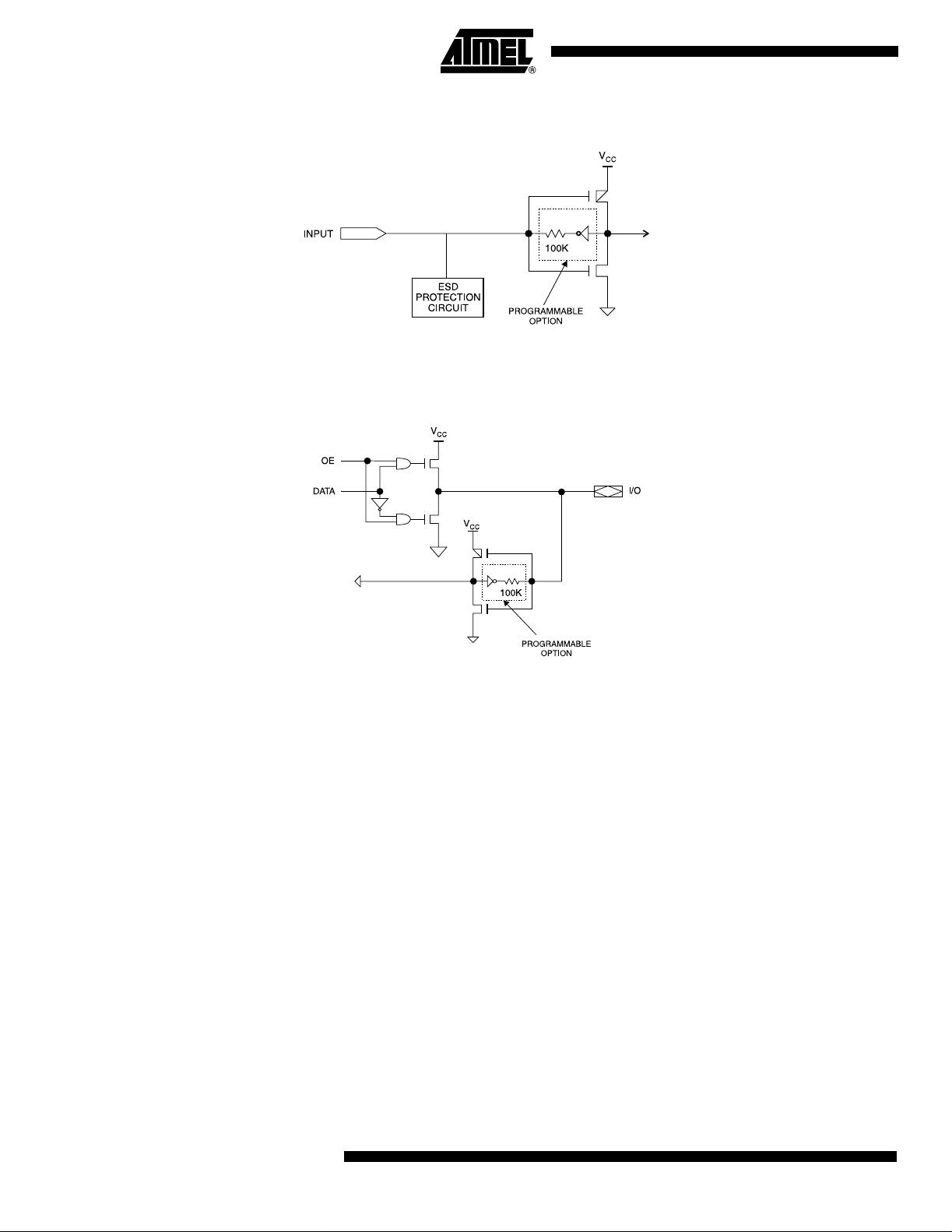
Input Diagram
I/O Diagram
Speed/Power Management
8
ATF1504ASV(L)
The ATF1504ASV(L) has several built-in speed and power management feat ur es. The
ATF1504ASV(L) co ntai ns circuitry that autom aticall y puts the device into a low power
standby mode when no lo gic transitions are oc curring. This not only reducespower consumption during inactive periods, but also provides proportional powersavi ngs for most
applications running at systemspeeds below 5 MHz. This feature may be selectedasa
device option.
To furtherreduc e power, eac h ATF1504ASV(L)macrocell has a reduced-powerbitfea-
ture. Thi s feature allows individual macrocells to be configured for maximum power
savings. This feature may be selectedasadesign option.
All ATF1504ASV(L)alsohave an optional power-down mode. In this mode,current
drops to below 5 mA. Whenthe power-dow n option is selected, either PD1 or PD2 pins
(or both) can be usedtopower down the part. The power-down option is selectedinthe
design source file. When enabled, the device goes into pow er down when either PD1 or
PD2 is high. In the pow er-down mode, all internal logic signals are latched and held, as
are any enabled outputs.
All pin transitions are ignored until thePDpin is brought low. Whenthe power-down fea-
ture is enabled, thePD1or PD2 pin c annot be used as a logic in put or output.However,
the pin’smacrocel l ma y still b e usedtogenerate buried foldback and cascade logic
signals.
1409H–PLD–09/02
Page 9

ATF1504ASV(L)
All power-down AC c haracteristic parameters are computedfromexternal inpu t or I/O
pins, with reduced-powerbitturnedon. For macrocells in reduced-powermode
(reduced-powerbitturned on), t he reduced-power adder, t
parameters, which include the data paths t
LAD,tLAC,tIC,tACL,tACH
The ATF1504ASV(L)macrocell also has an option whereby the powercanbe reduced
on a permacrocell basis. By enabling this power-down option, macrocells that are not
used in an application can be turned down, thereby reducing the overall power consumption of the device.
Each output also has individual slewrate co ntrol. This may be usedtoreduce s yst em
noise by slowing down outputs that do not needtooperate at maximum speed. Outputs
default to slow switching, and may be specified as f as t switching in the design file.
,mustbe addedtothe AC
RPA
and t
SEXP
.
Design So ft ware Support
ATF1504ASV(L)designs are s upportedbyseveral industry standard third party tools.
Automatedfitters allow logic s yn thesi s usi n g a variety of high-leveldescription languages and formats.
Power-up Reset The ATF1504ASV is designed with a power-up reset, a feature critical for state machine
initialization. At a point delayedslightlyfromV
tialized, and the state of each output will depend on the polarity of its buffer.However,
due to the asynchronous nature of resetanduncertainty of how V
system, the following conditions are required:
1. The V
rise must be monotonic,
CC
2. Afterreset occurs, all input and feedback setup timesmustbe metbefore dr iving
the clock pin high, and,
3. The c lock must remain stable during T
D
The ATF1504ASV has two options for the hysteresis about the resetlevel, V
and Large. To ensure a robust operating environment in applications where the device
is operatednear 3.0V, Atmelrecommends that during the fitting process users configure
the device with thePower-up Resethysteresis settoLarge. For conversions, A tmel
POF2JED users should i nc lude the flag “-power_reset” on the command line after “filename.POF”. To allow the registers to be properly reinitializedwiththeLarge hysteresis
option selected, the following condition is added:
4. If V
falls below 2.0V, it must shut off completely before the device is turnedon
CC
again.
.
crossing V
CC
,allregisters will be ini-
RST
actually risesinthe
CC
RST
,Small
WhentheLarge hysteresisoptionisactive,I
is reducedbyseveral hundredmicro-
CC
amps as well.
Security Fuse Usage Asingle fuse is providedtoprevent unau thorized copying of the ATF1504ASV(L)fuse
patterns. Onc e programmed, fuseverify is inhibited.However, the16-bit User Signature
remains accessible.
1409H–PLD–09/02
9
Page 10

Programming ATF1504ASV(L)devicesare in-system programma ble (ISP)devices utilizing the4-pin
JTAG protocol. This capability eliminates package handling normally required for programming and facilitates rapid d esign itera tio ns and field changes.
AtmelprovidesISP hardwa re and software to allow programming of the
ATF1504ASV(L) via thePC. ISP is performedbyusingeither a download cable,acom-
parable board testerorasimple microprocessor interface.
To facilitate ISP programming by the AutomatedTest Equipment (ATE) vendors. Serial
Vector Format (SVF) filescanbe createdbyAtmelprovidedsoftware utilities.
ATF1504ASV(L)devicescanalsobe programmed using standard third-party program-
mers. With thir d-party programmerthe JTAG ISP port can be disabledthereby allowing
four additional I/Opinstobe used for logic.
Contact you r local AtmelrepresentativesorAtmel PLD applications for details.
ISP Programming Protection
The ATF1504ASV(L) has a special feature that lock s the device and prevents the inputs
and I/O fro m driving if the prog ram ming p rocess is interru pted for any reason. The
inputs and I/Odefault to high-Z state during s uc h a condition. I n addition the pin keeper
option preservesthe formerstate during device prog ramming, if this circuit were previ-
ously programmedonthe device. This prevents disturbing the operation of other circuits
in the systemwhile the ATF1504ASV(L)isbeing programmed via ISP.
All ATF1504ASV(L)devicesare initially shipp edintheerasedstate thereby making
themready to use for ISP.
Note:Formore information refertothe“Designing for In-System Programmability with Atmel
CPLDs” application note.
10
ATF1504ASV(L)
1409H–PLD–09/02
Page 11

ATF1504ASV(L)
DC and AC Operating Conditions
Commercial Industrial
Operating Temperature (Ambient)) 0
V
(3.3V) Power Supply 3.0V-3.6V 3.0V-3.6V
CC
DC Characteristics
Symbol Parameter Condition Min Typ Max Units
I
IL
I
IH
I
OZ
I
CC1
I
CC2
I
CC3
V
IL
V
IH
V
OL
V
OH
Notes: 1. Not more than one output at a time should be shor ted.Duration of short circuit test should not exceed30 sec.
Input or I/O Low
LeakageCurrent
V
IN=VCC
Input or I/O High
LeakageCurrent
Tri-State Output
Off-State Current
V
or GND -40 40 µA
O=VCC
Com. 60 mA
Power Supply Current,
Standby
Power Supply Current,
Power-down Mode
Reduced-powerMode
(2)
Supply Current, Standby
VCC=Max
= 0,V
V
IN
VCC=Max
= 0,V
V
IN
VCC=Max
= 0,V
V
IN
Std Mode
CC
“L” Mode
“PD” Mode0.15mA
CC
Std Power
CC
Ind. 75 mA
Com. 5µA
Ind. 5µA
Com 40 ma
Ind 55
Input Low Voltage -0.3 0.8V
Input High Voltage1.7V
Output Low Voltage (TTL)
Output Low Voltage (CMOS)
Output High Voltage
-3.3V (TTL)
Output High Voltage
-3.3V (CMOS)
V
V
V
VCC=Min,IOL= 0.1 mA
VIN=VIHor V
V
V
V
or V
IN=VIH
CCIO
IN=VIH
CCIO
IN=VIH
CCIO
IL
=Min,IOL=8mA
or V
IL
IL
=Min,IOH=-2.0 mA
or V
IL
=Min,IOH=-0.1 mA
Com.0.45V
Ind.0.45
Com.0.2V
Ind.0.2V
V
2. Whenmicrocell reduced-powerfeature is enabled.
°C-70°C-40°C-85°C
-2 -10 µA
210
+ 0.3V
CCIO
2.4 V
- 0.2 V
CCIO
Pin Capacitance
Typ Max Units Conditions
C
IN
C
I/O
8pFV
8pFV
Note:Typicalvalues for nominal supply voltage. This parameter is only sampled and is not 100%tested.
The OGI pin (high-voltage pin during programming)has a maximum capacitance of 12 pF.
1409H–PLD–09/02
= 0V; f = 1.0 MHz
IN
= 0V;f=1.0 MHz
OUT
11
Page 12

Absolute Maximum Ratings*
Temperature UnderBias.................................. -40°Cto+85°C
Storage Temperature..................................... -65°Cto+150°C
Voltage on Any Pin with
Respect to Ground .........................................-2.0Vto+7.0V
Voltage on Input Pins
with Re spect to Ground
During Programming.....................................-2.0Vto+14.0V
ProgrammingVoltage with
Respect to Ground .......................................-2.0Vto+14.0V
Timing Model
Internal Output
Enable Delay
t
IOE
Global Control
Input
Delay
t
IN
Switch
Matrix
t
UIM
Delay
t
GLOB
Logic Array
Delay
t
LAD
Register Control
Delay
t
LAC
t
IC
t
EN
FoldbackTerm
Delay
t
SEXP
(1)
(1)
(1)
Cascade Logic
*NOTICE: Stressesbeyond those listed under “Absolute
Maximum Ratings” may cause permanent damage to the device. This is a stress rating only and
functionaloperation of the device at these or any
other conditions beyond those indicatedinthe
operational sections of this specification is not
implied. Exposure to absolute maximum rating
conditions for extendedperiods may affect
device reliability.
Note: 1. Minimum voltage is -0.6V DC, which may under-
shoot to -2.0V for pulsesofless than 20 ns. Max-
imum output pin voltage is V
+ 0.75V DC,
CC
which may overshoot to 7.0V for pulsesofless
than 20 ns.
Register
Delay
t
PEXP
Fast Input
Delay
t
FIN
Delay
t
SU
t
H
t
PRE
t
CLR
t
RD
t
COMB
t
FSU
t
FH
Output
Delay
t
OD1
t
OD2
t
OD3
t
XZ
t
ZX1
t
ZX2
t
ZX3
I/O
Delay
t
IO
12
ATF1504ASV(L)
1409H–PLD–09/02
Page 13

AC Characteristics
ATF1504ASV(L)
-15 -20
Symbol Parameter
t
PD1
t
PD2
t
SU
t
H
t
FSU
t
FH
t
COP
t
CH
t
CL
t
ASU
t
AH
t
ACOP
t
ACH
t
ACL
t
CNT
f
CNT
t
ACNT
f
ACNT
f
MAX
t
IN
t
IO
t
FIN
t
SEXP
t
PEXP
t
LAD
t
LAC
t
IOE
t
OD1
t
OD2
t
OD3
t
ZX1
Input or Feedback to Non-Registered Output 3 15 20 ns
I/O Input or Feedback to Non-RegisteredFeedback 3 12 16ns
Global Clock Setup Time1113.5ns
Global Clock Hold Time00ns
Global Clock Setup Time of Fast Input 3 3 ns
Global Clock Hold Time of FastInput 1.0 2 MHz
Global Clock to Output Delay 912ns
Global Clock High Time 56ns
Global Clock Low Time 56ns
Array Clock Setup Time 57ns
Array Clock Hold Ti me44ns
Array Clock Output Delay 15 18.5ns
Array Clock High Time 68ns
Array Clock Low Time 68ns
Minimum Clock Global Period 13 17ns
Maximum Internal Global Clock Frequency 76.9 66 MHz
Minimum Array Clock Period 13 17ns
Maximum Internal Array Clock Frequency 76.9 58.8MHz
Maximum Clock Frequency 100 83.3MHz
Input Pad and Buffer Delay 22.5ns
I/O Input Pad and Buffer Delay 22.5ns
Fast Input Delay 22ns
FoldbackTerm Delay 8 10 ns
CascadeLogic Delay 11ns
Logic Array Delay 6 8 ns
Logic Control Delay 3.5 4. 5ns
Internal Output EnableDelay 3 3 ns
Output Buffer and Pad Delay
(Slow slewrate = OFF; V
Output Buffer and Pad Delay
(Slow slewrate = OFF; V
Output Buffer and Pad Delay
(Slow slewrate =ON;V
Output Buffer EnableDelay
(Slow slewrate = OFF; V
=5V;CL=35pF)
CCIO
=3.3V; CL=35pF)
CCIO
=5Vor3.3V; CL=35pF)
CCIO
=5.0V; CL=35pF)
CCIO
UnitsMin Max Min Max
3 4 ns
3 4 ns
56ns
7 9 ns
1409H–PLD–09/02
13
Page 14

AC Characteristics (Continued)
Symbol Parameter
-15 -20
UnitsMin Max Min Max
t
ZX2
t
ZX3
t
XZ
t
SU
t
H
t
FSU
t
FH
t
RD
t
COMB
t
IC
t
EN
t
GLOB
t
PRE
t
CLR
t
UIM
t
RPA
Output Buffer EnableDelay
(Slow slewrate = OFF; V
=3.3V; CL=35pF)
CCIO
Output Buffer EnableDelay
(Slow slewrate =ON;V
=5.0V/3.3V; CL=35pF)
CCIO
Output Buffer DisableDelay (CL=5pF) 6 7 ns
RegisterSetup Time 56ns
Register Hold Time45ns
RegisterSetup Time of Fast I nput 22ns
Register Hold Time of Fast Input 22ns
Register Delay 22.5ns
Combinatorial Delay 2 3ns
Array Clock Delay 6 7 ns
Register Enable Time 67ns
Global Control Delay 2 3ns
Register PresetTime45ns
RegisterClear Time45ns
Switch Mat r ix Delay 22.5ns
Reduced-powerAdder
(2)
Notes: 1. See ordering information for valid part numbers.
2. The t
parametermustbe addedtothe t
RPA
LAD,tLAC,tTIC,tACL
powermode.
3. See ordering information for valid part numbers.
,andt
7 9 ns
10 11 ns
10 13ns
parameters for macrocells running in the reduced-
SEXP
Input Test Waveforms and Measurement Levels
tR,tF= 1.5nstypical
Output AC T est Loads
3.0V
R1 = 703Ω
OUTPUT
PIN
CL=35pFR2 = 8060Ω
14
ATF1504ASV(L)
1409H–PLD–09/02
Page 15

ATF1504ASV(L)
Power-down Mode The ATF1504ASV(L)includes an optional pin-controlledpower-down feature. Whenthis
mode is enabled, thePDpin acts as the power-down pin. WhenthePDpin is high, the
device supply c urrent is reducedtoless than 3 mA.During p ow er down, all output data
and internal logic statesare latchedinternally and held. Therefore,allregistered and
combinatorial output data rema in valid. Any outputs that were in a High-Z state at the
onset will remain at High-Z.During power down , all input signals except the power-down
pin are blocked. Input a nd I/O hold latchesremain active to ensure that pins do not float
to indeterminate levels, furtherreducing systempower. The power-down mode feature
is enabledinthe logic design file or as a fittedortranslateds/woption.Designs using
the power-down pin may not u se thePDpin as a logic array inp ut.However, all other PD
pin macrocell resourcesmaystillbe used, including the buriedfeedback and foldback
product term array inp uts.
Power Down AC Characteristics
Symbol Parameter
t
IVDH
t
GVDH
t
CVDH
t
DHIX
t
DHGX
t
DHCX
t
DLIV
t
DLGV
t
DLCV
t
DLOV
Notes: 1. For slow slew outputs, add t
Valid I, I/ObeforePDHigh 15 20 ns
Valid OE
Valid Clock
(2)
beforePDHigh 15 20 ns
(2)
beforePDHigh 15 20 ns
I, I/O Don’tCare after PD High 2530 ns
(2)
OE
Don’tCare after PD High 2530 ns
(2)
Clock
Don’tCare after PD High 2530 ns
PD Low to Valid I, I/O 11µs
PD Low to Valid OE (Pin or Term) 11µs
PD Low to Valid Clock (Pin or Term) 11µs
PD Low to Valid Output 11µs
.
SSO
2. Pin or product term.
3. Includest
for reduced-powerbitenabled.
RPA
(1)(2)
-15 -20
UnitsMin Max Min Max
1409H–PLD–09/02
15
Page 16

JTAG-BST/ISP Overview
The JTAG boundary-scan testing is controlledbythe Test Access Port (TAP)controller
in the ATF1504ASV(L). The boundary-s c an technique involvesthe inclusion of a shiftregisterstage (contained in a boundary - scan cell) adjacent to each component so that
signals at component boundariescanbe controlled and observed using scan testing
principles. Each input pin and I/O pin has its own boundary-sc an cell (BSC) in o rderto
support boundary-scan testing. The ATF1504ASV(L)doesnotcurrently include aTest
Reset(TRST) input pin because the TAP controller is automati cally resetatpower-up.
The five JTA G modes supportedinclude:SAMPLE/PRELOAD, EXTEST, BYPASS,
IDCODEandHIGHZ. The ATF1504ASV(L)’sISP can be fully describedusingJTAG’s
BSDL as descr ib ed in IEEE Standard 1149 . 1b. This allows ATF1504 ASV(L)programming to be descr i bed and i mplemented using any one of the third-party development
tools supporting this standard.
The ATF1504ASV(L) has the option of using four JTA G-s ta ndard I/O pins for boundaryscan testing (BST) and in-system programming (ISP) purposes. The ATF1504ASV(L)is
programmable through the four JTAG pins using the IEEE standa rd JTAG programming
protocol established by IEEE Standard 1149.1 using 5V TTL-level programming s ignals
from the IS P interface for in-system programming. The JT AG feature is a programmabl e
option. If JTAG (BST or ISP)isnotneeded, thenthe four JTAG control pins are available as I/Opins.
JTAG Boundary-scan Cell (BSC) Testing
BSC Configuration for Input and I/O Pins (Except JTAG TAP Pins)
The ATF1504AS V(L)containsupto68I/O pins and four in put pins, dependingonthe
device type an d package type selected. Each input pin and I/O pin has its own boundary-scan cell (BSC) in order to support boundary-scan testing as describedindetail by
IEEE Standard 1149.1. A typical BSC consists of three capture registers or scan registers and up to two update registers. There are two types of BSCs, one for input o r I/O
pin, and on e for the macrocells. The BSCs in the device are chainedtogether through
the capture registers. Input to the capture register chain is fedinfromthe TDI pin while
the output is directedtothe TDOpin. C apture registers are used to capture active
devicedata signals, to shift data in and out of the device and to load data into the update
registers. Cont rol signals are generatedinternally by the JTAG TAP con troller. The BSC
configuration for the input and I/O pins and macrocells are shown below.
16
Note:The ATF1504ASV(L) has pull-up option on TMS and TDIpins. This feature is selectedas
adesign option.
ATF1504ASV(L)
1409H–PLD–09/02
Page 17

BSC Configuration for Macrocell
ATF1504ASV(L)
Pin BSC
TDO
OEJ
OUTJ
Pin
TDO
0
1
0
1
DQ
DQ
0
1
TDI
Shift
DQ
DQ
Capture
Clock
DQ
DR
0
1
0
1
Pin
1409H–PLD–09/02
TDI
Shift
Capture
DR
Macrocell BSC
Update
DR
Mode
Clock
17
Page 18

ATF1504ASV Dedicated Pinouts
44-lead
Dedicated Pin
INPUT/OE2/GCLK2 40 2 2 2 92 90
INPUT/GCLR 391 1 19189
INPUT/OE1 38 44 68 849088
INPUT/GCLK1 37 43678389 87
I/O /GCLK3 35 41 65 81 87 85
I/O /PD(1,2)5,19 11, 25 17, 37 20, 46 14, 44 12, 42
I/O / TDI(JTAG) 1 7 12 14 6 4
I/O / TMS (JTAG) 7 13 19 23 17 15
I/O / TCK (JTAG) 2632 50 62 64 62
I/O / TDO(JTAG) 32 38 57 71 75 73
GND4, 16, 24,36 10, 22,30, 42
V
CC
N/C ––––
TQFP
9, 17, 29, 41 3, 15, 23, 35
44-lead
J-lead
68-lead
J-lead
6, 16, 26, 34,
38, 48, 58, 66
3, 11, 21,31,
35, 43, 53, 63
84-lead
J-lead
7, 19,32, 42,
47, 59,72,82
3,13, 26, 38,
43, 53, 66, 78
100-lead
PQFP
13, 28, 40, 45,
61, 76, 88, 97
5, 20, 36, 41,
53, 68, 84, 93
1, 2,7,9,
24, 26, 29,30,
51,52, 55, 57,
72,74,79,80
100-lead
TQFP
11, 26, 38, 43,
59,74,86,95
3, 18, 34,39,
51, 66, 82, 91
1, 2,5,7,22,
24, 27, 28, 49,
50, 53, 55, 70,
72, 77, 78
# of Signal Pins 36 36 52 68 68 68
#UserI/O Pins 32 324864 64 64
OE (1, 2) Global OE pins
GCLR Global Clear pin
GCLK(1, 2, 3) Global Clock pins
PD (1, 2) Power-down pins
TDI, TMS, TCK, TDOJTAGpinsused for boundary-scan testing or in-system programming
GND Ground pins
VCC VCC pins for the device
18
ATF1504ASV(L)
1409H–PLD–09/02
Page 19

ATF1504ASV(L)
ATF1504ASV I/O Pinouts
44-lead
MC PLC
1 A 12 6 18 22 16 14 33 C 24 183644 42 40
2 A- - -21 15 1334 C---45 43 41
3
4 A 9 3 15 18 12 10 36 C 26 20 3948 46 44
5A8 21417 11 9 37 C 27 21 40 49 47 45
6A - -13 16 10 838C - -41 5048 46
7A - - -158 639 C---514947
8/
TDI
9 A- -10 12 4 100 41 C 29 23 44 54 54 52
10 A-- -11 3 99 42 C - - - 55 56 54
11 A644 9 10 100 98 43C - -45565856
12 A--899997 44 C--465759 57
13A - - 7 8 98 96 45C - -475860 58
14 A5435 696 94 46C3125 49 60 62 60
15A - - - 5 95 93 47C - - -61 63 61
16A 4424 49492
17B21 153341 39 37 49 D 33 2751 63 65 63
18B - - - 40 38 36 50D ---64 66 64
19 B 20 14 32 39 37 35 51D342852 65 67 65
20 B 19 1330 37 35 33 52D36 30 54 67 69 67
21 B 18 12 29 36 34 32 53 D 37 31 55 68 70 68
22 B--28353331 54D --5669 71 69
23B - - - 34 32 30 55 D ---70 73 71
24 B 17 11 27333129
25B16 10 253127 2357 D 39 33 59 73 77 75
26B - - - 3025 22 58 D ---74 78 76
27B - - 24 29 23 21 59D --60 75 81 79
28B - - 23 28 22 20 60D --61 76 82 80
29 B--22 27 21 19 61D --62 77 83 81
30 B 14 8 20 25 19 1762D4034 64 79 85 83
31 B- - -24 18 1663 D ---80 86 84
32/
TMS
PLCC
A/
PD1
A7112146 440C 28 22 42 52 5048
B 13719 23 17 1564
44-lead
TQFP
11 5 17 20 14 12 35
68-lead
PLCC
84-lead
PLCC
100lead
PQFP
100lead
TQFP MC PLC
C/
PD2
48/
TCK
56/
TDO
C322650 62 64 62
D 38 32 57 71 75 73
D/
GCLK3
44-lead
44-lead
PLCC
TQFP
25 19 37 46 44 42
41 35 65 81 87 85
68-lead
PLCC
84-lead
PLCC
100lead
PQFP
100lead
TQFP
1409H–PLD–09/02
19
Page 20

SUPPLY CURRENT VS. SUPPLYVOLTAGE
(T
= 25°C,F = 0)
A
100
75
(mA)
50
CC
I
25
0
2.502.75 3.00 3.253.50 3.75 4.00
STANDARD POWER
REDUCEDPOWER MODE
SUPPLYVOLTAGE (V)
SUPPLYCURRENT VS. FREQUENCY
LOW-POWER ("L") VERSION
(T
= 25°C)
A
100.0
80.0
60.0
(mA)
CC
I
40.0
20.0
0.0
0.00 5.00 10.00 15.00 20.00
FREQUENCY (MHz)
STANDARD POWER
REDUCEDPOWER
SUPPLY CURRENT VS. SUPPLY VOLTAGE
PIN-CONTROLLEDPOWER-DOWN MODE
(T
= 25°C,F = 0)
800
700
600
ICC (uA)
500
400
2.502.75 3.00 3.253.50 3.75 4.00
A
STANDARD & REDUCEDPOWER MODE
SUPPLYVOLTAGE (V)
SUPPLY CURRENT VS. FREQUENCY
STANDARD POWER (T
150.0
125.0
100.0
(mA)
75.0
CC
I
50.0
25.0
0.0
0.00 20.00 40.00 60.00 80.00 100. 00
STANDARD POWER
FREQUENCY(MHz)
= 25°C)
A
REDUCE DPOWER MODE
OUTPUT SOURCE CURRENT
VS.SUPPLYVOLTAGE
(V
=2.4V,TA= 25°C)
0
-2
-4
-6
(mA)
-8
OH
I
-10
-12
-14
-16
2.75 3.00 3.253.50 3.75 4.00
OH
SUPPLY VOLTAGE(V)
OUTPUT SOURCE CURRENT
VS. OUTPUT VOLTAGE
(V
=3.3V,TA= 25°C)
10
0
-10
-20
(mA)
-30
OH
I
-40
-50
-60
-70
0.0 0.5 1.0 1.5 2.0 2.53.0 3.5 4.0
CC
OUTPUT VOLTAGE(V)
20
SUPPLY CURRENT VS. SUPPLYVOLTAGE
LOW-POWER ("L") VERSION
(T
= 25°C,F = 0)
25
20
15
ICC (uA)
10
5
0
2.502.75 3.00 3.253.50 3.75 4.00
A
SUPPLYVOLTAGE (V)
ATF1504ASV(L)
OUTPUT SINK CURRENT VS. SUPPLY VOLTAGE
=0.5V,TA= 25°C)
(V
40
35
(mA)
30
OL
I
25
20
2.75 3.00 3.253.50 3.75 4.00
OL
SUPPLY VOLTAGE (V)
1409H–PLD–09/02
Page 21

ATF1504ASV(L)
OUTPUT SINK CURRENT VS. OUTPUT VOLTAGE
=3.3V,TA= 25°C)
(V
100
80
60
(mA)
OL
I
40
20
0
00.5 11.5 22.533.5 4
CC
OUTPUTVOLTAGE (V)
INPUT CLAMP CURRENT VS.INPUT VOLTAGE
(V
=3.3V,TA= 25°C)
0
-20
-40
-60
-80
INPUT CURRENT (mA)
-100
-1 -0.9 -0.8-0.7-0.6-0.5-0.4 -0.3-0.2 -0.1 0
CC
INPUT VOLTAGE (V)
INPUT CURRENT VS. INPUT VOLTAGE
=3.3V,TA= 25°C)
(V
15
10
5
0
INPUT CURRENT (uA)
-5
-10
00.5 11.5 22.533.5
CC
INPUT VOLTAGE (V)
1409H–PLD–09/02
21
Page 22

ATF1504ASV(L) Ordering Information
t
PD
(ns)
158 100 ATF1504ASV-15AC44
158 100 ATF1504ASV-15AI44
20 12 83.3ATF1504ASVL-20 AC44
20 12 83.3ATF1504ASVL-20 AI44
t
CO1
(ns)
f
MAX
(MHz) Ordering Code Package Operation Range
ATF1504ASV-15JC44
ATF1504ASV-15JC68
ATF1504ASV-15JC84
ATF1504ASV-15QC100
ATF1500ASV-15AC100
ATF1504ASV-15JI44
ATF1504ASV-15JI68
ATF1504ASV-15JI84
ATF1504ASV-15QI100
ATF1504ASV-15AI100
ATF1504ASVL-20 JC44
ATF1504ASVL-20 JC68
ATF1504ASVL-20 JC84
ATF1504ASVL-20 QC100
ATF1504ASVL-20 AC100
ATF1504ASVL-20 JI44
ATF1504ASVL-20 JI68
ATF1504ASVL-20 JI84
ATF1504ASVL-20 QI100
ATF1504ASVL-20 AI100
44A
44J
68J
84J
100Q1
100A
44A
44J
68J
84J
100Q1
100A
44A
44J
68J
84J
100Q1
100A
44A
44J
68J
84J
100Q1
100A
Commercial
(0°Cto70°C)
Industrial
(-40°Cto+85°C)
Commercial
(0°Cto70°C)
Industrial
(-40°Cto+85°C)
Using “C” Product for Industrial
There is very little risk in using “C” devices for industrial applications because the VCCconditions for 3.3V products are the
same for commercial and industrial (there is only 15°Cdifference at the high end of the temperature range). To use com-
mercial product for industrial temperature ranges, de-rate I
22
ATF1504ASV(L)
by 15%.
CC
1409H–PLD–09/02
Page 23

Packaging Information
44A – TQFP
PIN 1
ATF1504ASV(L)
B
PIN 1 IDENTIFIER
e
E1 E
D1
D
C
0˚~7˚
A1
L
Notes: 1. This package conforms to JEDEC reference MS-026, Variation ACB.
2. Dimensions D1 and E1 do not include mold protrusion. Allowable
protrusion is 0.25 mm per side. Dimensions D1 and E1 are maximum
plastic body size dimensions including mold mismatch.
3. Lead coplanarity is 0.10 mm maximum.
A2 A
SYMBOL
COMMON DIMENSIONS
(Unit of Measure = mm)
MIN
A – – 1.20
A1 0.05 – 0.15
A2 0.95 1.00 1.05
D 11.75 12.00 12.25
D1 9.90 10.00 10.10 Note 2
E 11.75 12.00 12.25
E1 9.90 10.00 10.10 Note 2
B 0.30 – 0.45
C 0.09 – 0.20
L 0.45 – 0.75
e 0.80 TYP
NOM
MAX
NOTE
2325 Orchard Parkway
R
San Jose, CA 95131
1409H–PLD–09/02
TITLE
44A, 44-lead, 10 x 10 mm Body Size, 1.0 mm Body Thickness,
0.8 mm Lead Pitch, Thin Profile Plastic Quad Flat Package (TQFP)
10/5/2001
DRAWING NO.
44A
REV.
B
23
Page 24

44J–PLCC
1.14(0.045) X 45°
B
e
0.51(0.020)MAX
45° MAX (3X)
Notes: 1. This package conforms to JEDEC reference MS-018, Variation AC.
2. Dimensions D1 and E1 do not include mold protrusion.
Allowable protrusion is .010"(0.254 mm) per side. Dimension D1
and E1 include mold mismatch and are measured at the extreme
material condition at the upper or lower parting line.
3. Lead coplanarity is 0.004" (0.102 mm) maximum.
PIN NO. 1
IDENTIFIER
D1
D
1.14(0.045) X 45°
E1 E
0.318(0.0125)
0.191(0.0075)
NOM
D2/E2
MAX
B1
A2
A1
A
COMMON DIMENSIONS
(Unit of Measure = mm)
SYMBOL
A 4.191 – 4.572
A1 2.286 – 3.048
A2 0.508 – –
D 17.399 – 17.653
D1 16.510 – 16.662 Note 2
E 17.399 – 17.653
E1 16.510 – 16.662 Note 2
D2/E2 14.986 – 16.002
B 0.660 – 0.813
B1 0.330 – 0.533
e 1.270 TYP
MIN
NOTE
24
2325 Orchard Parkway
R
San Jose, CA 95131
44J, 44-lead, Plastic J-leaded Chip Carrier (PLCC)
ATF1504ASV(L)
TITLE
DRAWING NO.
44J
1409H–PLD–09/02
10/04/01
REV.
B
Page 25

68J–PLCC
ATF1504ASV(L)
1.14(0.045) X 45°
B
e
0.51(0.020)MAX
45° MAX (3X)
Notes: 1. This package conforms to JEDEC reference MS-018, Variation AE.
2. Dimensions D1 and E1 do not include mold protrusion.
Allowable protrusion is .010"(0.254 mm) per side. Dimension D1
and E1 include mold mismatch and are measured at the extreme
material condition at the upper or lower parting line.
3. Lead coplanarity is 0.004" (0.102 mm) maximum.
PIN NO. 1
IDENTIFIER
D1
D
1.14(0.045) X 45°
E1 E
0.318(0.0125)
0.191(0.0075)
NOM
D2/E2
MAX
B1
A2
A1
A
COMMON DIMENSIONS
(Unit of Measure = mm)
SYMBOL
A 4.191 – 4.572
A1 2.286 – 3.048
A2 0.508 – –
D 25.019 – 25.273
D1 24.130 – 24.333 Note 2
E 25.019 – 25.273
E1 24.130 – 24.333 Note 2
D2/E2 22.606 – 23.622
B 0.660 – 0.813
B1 0.330 – 0.533
e 1.270 TYP
MIN
NOTE
R
1409H–PLD–09/02
2325 Orchard Parkway
San Jose, CA 95131
TITLE
68J, 68-lead, Plastic J-leaded Chip Carrier (PLCC)
DRAWING NO.
68J
10/04/01
REV.
B
25
Page 26

84J–PLCC
1.14(0.045) X 45°
B
e
0.51(0.020)MAX
45° MAX (3X)
Notes: 1. This package conforms to JEDEC reference MS-018, Variation AF.
2. Dimensions D1 and E1 do not include mold protrusion.
Allowable protrusion is .010"(0.254 mm) per side. Dimension D1
and E1 include mold mismatch and are measured at the extreme
material condition at the upper or lower parting line.
3. Lead coplanarity is 0.004" (0.102 mm) maximum.
PIN NO. 1
IDENTIFIER
D1
D
1.14(0.045) X 45°
E1 E
0.318(0.0125)
0.191(0.0075)
NOM
D2/E2
MAX
B1
A2
A1
A
COMMON DIMENSIONS
(Unit of Measure = mm)
SYMBOL
A 4.191 – 4.572
A1 2.286 – 3.048
A2 0.508 – –
D 30.099 – 30.353
D1 29.210 – 29.413 Note 2
E 30.099 – 30.353
E1 29.210 – 29.413 Note 2
D2/E2 27.686 – 28.702
B 0.660 – 0.813
B1 0.330 – 0.533
e 1.270 TYP
MIN
NOTE
26
2325 Orchard Parkway
R
San Jose, CA 95131
84J, 84-lead, Plastic J-leaded Chip Carrier (PLCC)
ATF1504ASV(L)
TITLE
DRAWING NO.
84J
1409H–PLD–09/02
10/04/01
REV.
B
Page 27

100Q1 – PQFP
Dimensions in Millimeters and (Inches)*
*Controlling dimensions: millimeters
JEDEC STANDARD MS-022, GC-1
ATF1504ASV(L)
PIN1ID
0.65 (0.0256) BSC
0.40 (0.016)
0.22 (0.009)
0.23 (0.009)
0º~7º
0.11 (0.004)
PIN 1
17.45 (0.687)
16.95 (0.667)
14.12 (0.556)
13.90 (0.547)
1.03 (0.041)
0.73 (0.029)
20.10 (0.791)
19.90 (0.783)
23.45 (0.923)
22.95 (0.904)
3.40 (0.134) MAX
0.50 (0.020)
0.25 (0.010)
R
1409H–PLD–09/02
2325 Orchard Parkway
San Jose, CA 95131
TITLE
100Q1, 100-lead, 14 x 20 mm Body, 3.2 mm Footprint, 0.65 mm Pitch,
Plastic Quad Flat Package (PQFP)
04/11/2001
DRAWING NO.
100Q1
REV.
A
27
Page 28

100A – TQFP
PIN 1
B
PIN 1 IDENTIFIER
e
E1 E
D1
D
C
0˚~7˚
A1
L
Notes: 1. This package conforms to JEDEC reference MS-026, Variation AED.
2. Dimensions D1 and E1 do not include mold protrusion. Allowable
protrusion is 0.25 mm per side. Dimensions D1 and E1 are maximum
plastic body size dimensions including mold mismatch.
3. Lead coplanarity is 0.08 mm maximum.
A2 A
SYMBOL
COMMON DIMENSIONS
(Unit of Measure = mm)
MIN
A ––1.20
A1 0.05 – 0.15
A2 0.95 1.00 1.05
D 15.75 16.00 16.25
D1 13.90 14.00 14.10 Note 2
E 15.75 16.00 16.25
E1 13.90 14.00 14.10 Note 2
B 0.17 – 0.27
C 0.09 – 0.20
L 0.45 – 0.75
e 0.50 TYP
NOM
MAX
NOTE
28
2325 Orchard Parkway
R
San Jose, CA 95131
100A, 100-lead, 14 x 14 mm Body Size, 1.0 mm Body Thickness,
0.5 mm Lead Pitch, Thin Profile Plastic Quad Flat Package (TQFP)
ATF1504ASV(L)
TITLE
10/5/2001
DRAWING NO.
100A
1409H–PLD–09/02
REV.
C
Page 29

Atmel Headquarters Atmel Operations
Corporate Headquarters
2325 Orchard Parkway
San J ose,CA95131
TEL1(408) 441-0311
FAX 1(408) 487-2600
Europe
AtmelSarl
Route desArsenaux 41
CasePostale 80
CH-1705 Fribourg
Switzerland
TEL (41) 26-42 6-55 55
FAX ( 41) 26-426-55 00
Asia
Room 1219
Chinach emGolden Plaz a
77 Mod y Road Tsims hatsui
East Kowloon
Hong Kong
TEL (852) 2721-9778
FAX (85 2) 2722-1369
Japan
9F, Tonetsu Sh inkaw a Bldg.
1-24-8 Sh inkawa
Chuo-ku, Tokyo 104-0033
Japan
TEL (81)3-3523-3551
FAX ( 81)3-3523-75 81
Memory
2325 Orchard Parkw ay
San Jose,CA95131
TEL1(408) 441-0311
FAX 1(408) 436-4314
Microcontrollers
2325 Orchard Parkw ay
San Jose,CA95131
TEL1(408) 441-0311
FAX 1(408) 436-4314
La Chantrerie
BP 70602
44306NantesCedex3,France
TEL (33) 2-40-18-18-18
FAX (33) 2-40-18-19-60
ASIC/ASSP/Smart Cards
Zone Indus trielle
13106 RoussetCedex, France
TEL (33) 4-42-53-6 0-00
FAX (33) 4-42-53-60-01
1150 East Cheyenne Mtn. Blvd.
Colorado Springs, C O 8 0906
TEL1(719) 576-3300
FAX 1(719 )540 -1759
Scottish Enterp rise Techno logy Park
Maxwell Building
East Kilbride G75 0QR,Scotland
TEL (44) 1355-803-00 0
FAX (44) 13 55-24 2-743
RF/Automotive
Theresi enstrasse2
Postf ach 3535
74025 Heilbronn, Germany
TEL (49)71-31-67-0
FAX ( 49)71-31-67-2340
1150 Ea st Cheyenne Mtn. Blvd.
Colorado Spring s, CO 80906
TEL1(719)576-3300
FAX 1(719)540-1759
Biometrics/Imaging/Hi-Rel MPU/
High Speed Converters/RF Datacom
Avenue deRochepl eine
BP123
38521 Saint-Egreve Cedex, France
TEL (33) 4-76-58 -30-00
FAX (33 ) 4-76- 58-34-80
e-mail
literature@atmel.com
Web Site
http://www.atmel.com
© Atmel Corpor ation 2002.
Atmel C orpo rat io n makesnowarrantyforthe use of its products, other than tho seexpressly containedinthe C om p any’s standard wa rr an t y
which is detailedinAtmel’sTerms and Condi t io ns l oc atedonthe Co mpany’swebsite. The Company assu m esnoresponsibility for any erro rs
which may appear in this docum ent, reservesthe r igh t to c ha nge devicesorspecifications detai ledherein at any time without notice, and does
not make any co mmitm ent to update the information containedherein. No licensestopatents or otherintellectual property of Atmelare gr anted
by the Company in co nnectionwiththe sale of Atmelproducts,exp r essly or by implication. Atmel’sproductsare not authori zedforuse as cr itical
components in life support devices o r systems.
ATMEL®is the regi steredtrademark of Atmel.
Otherterms and product namesmaybe the trademarks of others.
Printedonrecycledpaper.
1409H–PLD–09/02 xM
 Loading...