

Page 1

Features
• High-density, High-performance, Electrically- erasable Complex Programmable
Logic Device
– 3.0 to 3.6V Operating Range
– 32 Macrocell s
– 5 Product Terms per Macrocell, Expandable up to 40 per Macrocell
–44Pins
–15nsMaximumPin-to-pinDelay
– Registered Operation up to 77 MHz
– Enhanced Routing Resources
• In-System Programmability (ISP) via JTAG
• Flexible Logic Macrocell
– D/T Latch Configurable Flip-flops
– Global and Individual Register Control Signals
– Global and Individual Output Enable
– Programmable Output Slew Rate
– Programmable Output Open Collector Option
– Maximum Logic Utilization by Burying a Register with a COM Output
• Advanced Power Management Features
– Pin-controlled 0.75 mA Standby Mode
– ProgrammablePin-keeper Inputs and I/Os
– Reduced-power Feature per Macrocell
• Avai lable in Commercial and Industrial Temperature Ranges
• Avai lable in 44-lead PLCC and TQFP
• Advanced EEPROM Technol o gy
– 100% Tested
– Completely Reprogrammable
– 10,000 Program/Erase Cycles
– 20-year Data Retention
– 2000V ESD Protection
– 200 mA Latch-up Immunity
• JTAG Boundary-scan Testing to IEEE Std. 1149.1-1990 and 1149.1a-1993 Support ed
• PCI-compliant
• Security Fuse Feature
Highperformance
EEPROM CPLD
ATF1502ASV
Enhanced Features
• ImprovedConnectivity (Additional Feedback Routing, Alternate Input Routing)
• Output Enable Product Ter ms
• D Latch Mode
• Combinatorial Output with Registered Feedback within Any Macrocell
• Three Global Clock Pins
• Fast Registered Input from Product Term
• Programmable“Pin-keeper” Option
• V
Power-up Reset Option
CC
• Pull-up Option on JTAG Pins TMS and TDI
• Advanced Power Management Features
– Individual Macrocell Power Option
Rev. 1615G–PLD–09/02
1
Page 2
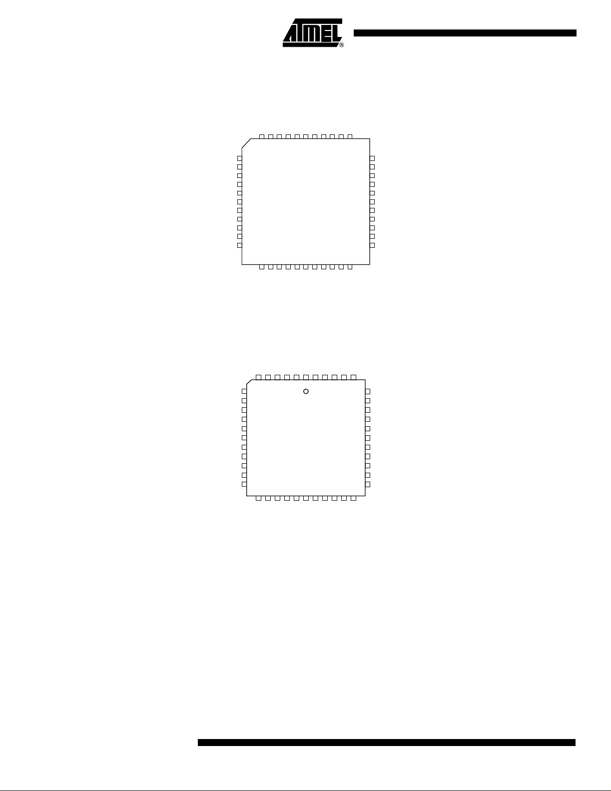
I/O/TDI
GND
PD1/I/O
TMS/I/O
VCC
I/O
I/O
I/O
I/O
I/O
I/O
44-lead TQFP
Top View
I/O
I/O
I/O
VCC
GCLK2/OE2/I
GCLR/I
4443424140393837363534
1
2
3
4
5
6
7
8
9
10
11
1213141516171819202122
I/O
I/O
I/O
I/O
VCC
GND
44-lead PLCC
Top View
I/OE1
I/O
GCLK1/I
GND
I/O
PD2/I/O
GCLK3/I/O
I/O
33
32
31
30
29
28
27
26
25
24
23
I/O
I/O
I/O
I/O/TDO
I/O
I/O
VCC
I/O
I/O
I/O/TCK
I/O
GND
I/O
I/O
I/O
I/O
VCC
GCLK2/OE2/I
GCLR/I
OE1/I
GCLK1/I
GND
GCLK3/I/O
I/O
TDI/I/O
I/O
I/O
GND
PD1/I/O
I/O
I/O/TMS
I/O
VCC
I/O
I/O
65432
7
8
9
10
11
12
13
14
15
16
17
1819202122232425262728
I/O
I/O
I/O
I/O
GND
1
VCC
4443424140
I/O
I/O
I/O
PD2/I/O
39
38
37
36
35
34
33
32
31
30
29
I/O
I/O
I/O/TDO
I/O
I/O
VCC
I/O
I/O
I/O/TCK
I/O
GND
I/O
Description The ATF1502ASV is a high-performance, high-density complex programmable logic
device (CPLD) that utilizes Atmel’s proven electrically-erasable technology. With 32
logic macrocells and up to 36 inputs, it easily integrates logic from several TTL, SSI,
MSI, LSI and classic PLDs. The ATF1502ASV’s enhanced routing switch matrices
increase usable gate count and the odds of successful pin-locked design modifications.
The ATF1502ASV has up to 32 bi-directional I /O pins and four dedicated input pins,
depending o n the type o f device package selected. Each dedicated pin can also serve
as a global control signal, registe r clock, regi ster reset or output enable. Each of these
control signals can be selected for use individua lly within each macrocell.
2
ATF1502ASV
1615G–PLD–09/02
Page 3

Block Diagram
ATF1502ASV
B
32
Each of the 32 m acrocells generates a buried feedback that goes to the global bus.
Each input and I/O pin also feeds into the global bus. The switch matrix in each logic
block then selects 40 individual signals from the global bus. Each macrocell also generates a foldb ack l ogic term t hat g oes to a regional bus. C asca de l ogic between
macrocells in the ATF1502ASV allows fast, efficient generation of comp lex logic func tions. The ATF1502ASV contains four such logic chains, each capable of creating sum
termlogicwithafan-inofupto40 product terms.
The ATF1502ASV macrocell, shown in Figure 1, is flexible enough to support highly
complex logic funct ions operating at high speed. The macrocell c ons ists of five sections:
product terms and product term select multiplexer, OR/XOR/CASCADE logic, a flip-flop,
output select and enable, and logic array inputs.
1615G–PLD–09/02
Unused product terms are automatically disabled by the compiler to decrease power
consumption. A security fuse, when programmed, protects the contents of the
ATF1502ASV. Two bytes (16 bits) of User Signature are accessible to the user for purposes such as sto ring project name, part number, revision or date. The User Signature
is accessible regardless of the state of the sec urity fuse.
The ATF1502ASV device is an in-system programmable (ISP) device. It uses the i ndustry standard 4-pin JTAG interface (IEEE Std. 1149.1), and is fully compliant with JTAG’s
3
Page 4
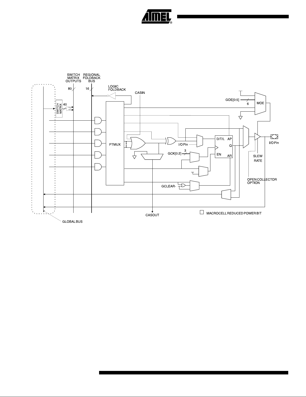
Figure 1. ATF1502ASV Macrocell
Boundary-scan Description Language (BSDL). ISP allows the dev ice to be programmed
without removing it from the printed circuit board. In addition to simplifying the manufacturing flow, ISP also allows design modifications to be made in the f ield via sof tware.
Product Terms and Select Mux
OR/XOR/ CASCADE Logic
4
ATF1502ASV
Each ATF1502ASV m ac r oc ell has five product terms. Each product term receives as its
inputs all signals from both the global bus and regional bus.
The product term select multiplexer (PTMUX ) allocates the five product terms as
needed to the macrocell logic gates and control signals. The PTMUX programming is
determined by the design compiler, which selects the optimum macrocell configuration.
The ATF1502ASV’s logic struc ture is design ed to efficiently suppo rt all types of logic.
Within a single macrocell, all the product terms can be routed to the O R gate, creating a
5-input AND/OR s um term. With the addition of the CA SIN from neighboring macrocells,
this can be expanded to as many as 40 product terms with little additional delay.
The macrocell’s XOR gate allows efficient implementation of compare and arithmetic
functions. One input t o the XOR comes from the OR sum term. The other XOR input c an
be a p roduct term or a fixed high or low level. For combinatorial outputs, the fixed level
input allows polarity selection. For registered functions, the fixed levels allow DeMorgan
minimization of product terms. The XOR gate is also used to emulate T- and JK-type
flip-flops.
1615G–PLD–09/02
Page 5

ATF1502ASV
Flip-flop The ATF1502ASV’s flip-flop h as very flexible data and control functions. The dat a input
cancomefromeithertheXOR gate , fr om a separate product term or directly from the
I/O pin . Selecting the separate product term all ows creation of a buried registered feedback within a combinatorial output macroc ell . (This feature is automatically implemented
by the fitter software). In addition to D, T, JK and SR operation, the flip-flop can also be
configured as a flow-through latch. In this mode, data passes through when the clock is
high and is latched when the clock is low.
The clock itself can be either one of the Global CLK signals (GCK[0 : 2]) or an individual
product term. The flip-flop changes state on the clock’s rising edge. When the GCK signal is used as the clock, one of the macrocell product terms can be selected as a clock
enable. When the clock enable function is active and the enable signal (p ro duc t term) is
low, all clock edges are ignored. The flip-flop’s asynchronous reset signal (AR) can be
either the Global Clear (GCLEAR), a product term, or always off. AR can also be a logic
OR of GCLEAR with a product term. The asynchronous preset (AP) can be a product
term or always off.
Extra Feedback The ATF1502ASV macrocell output can be selected as registered or combinatorial.The
extra burie d feedback signal can be either com binatorial or a regist ered signal regardless of whether the output is combinatorial or registered. (This enhancement function is
autom atical ly implemented by t he fitter soft ware.) Feedback of a buried combinatorial
output allow s the creation of a second latch within a macrocell.
I/O Control The outpu t enable multiplexer (MOE) controls the out put enable signal. Each I/O can be
individually configured as an input, output or for bi-directional operation. The output
enable for each macrocell can be selected from the true or compliment of the t wo output
enable pins, a subset of the I/O pins, or a subset of the I/O macroc ells. This selection is
automatically done by the fitter software when the I/O is configured as an input, all macrocell resources are still av ailab le, including the buried feedback, expander and cas ca de
logic.
Global Bus/Switch Matrix The global bus contains all i nput and I/O pin signals as well as the buried feed bac k sig-
nal from all 32 macrocells. The switch matrix in each logic block receives as its inputs all
signals from the global bus. Under software control, up to 40 of these signals can be
selected as inputs to the logic block.
Foldback Bus Each macrocell also generates a foldback product term. This signal goes to the regional
bus and is available to four macrocells. The foldback i s an inverse polarity of one of the
macro cell’s product term s . The four foldback ter ms in each region allow generation of
high fan-in sum terms (up to nine product terms) with little additional delay.
Programmable Pinkeeper Option for
Inputs and I/Os
The ATF1502ASV offers the option of programming all input and I/O pins so that pinkeeper circuits can be utilized. When any pin is driven high or low and then subsequently left floating , it will stay at that previous high or low level. This circuitry prevent s
unused input and I/O lines from floating to intermediate voltage levels, which causes
unnecessary power consumption and system noise. The keeper circuits eliminate the
need for external pull-up resistors and eliminate their DC power consumption.
1615G–PLD–09/02
5
Page 6
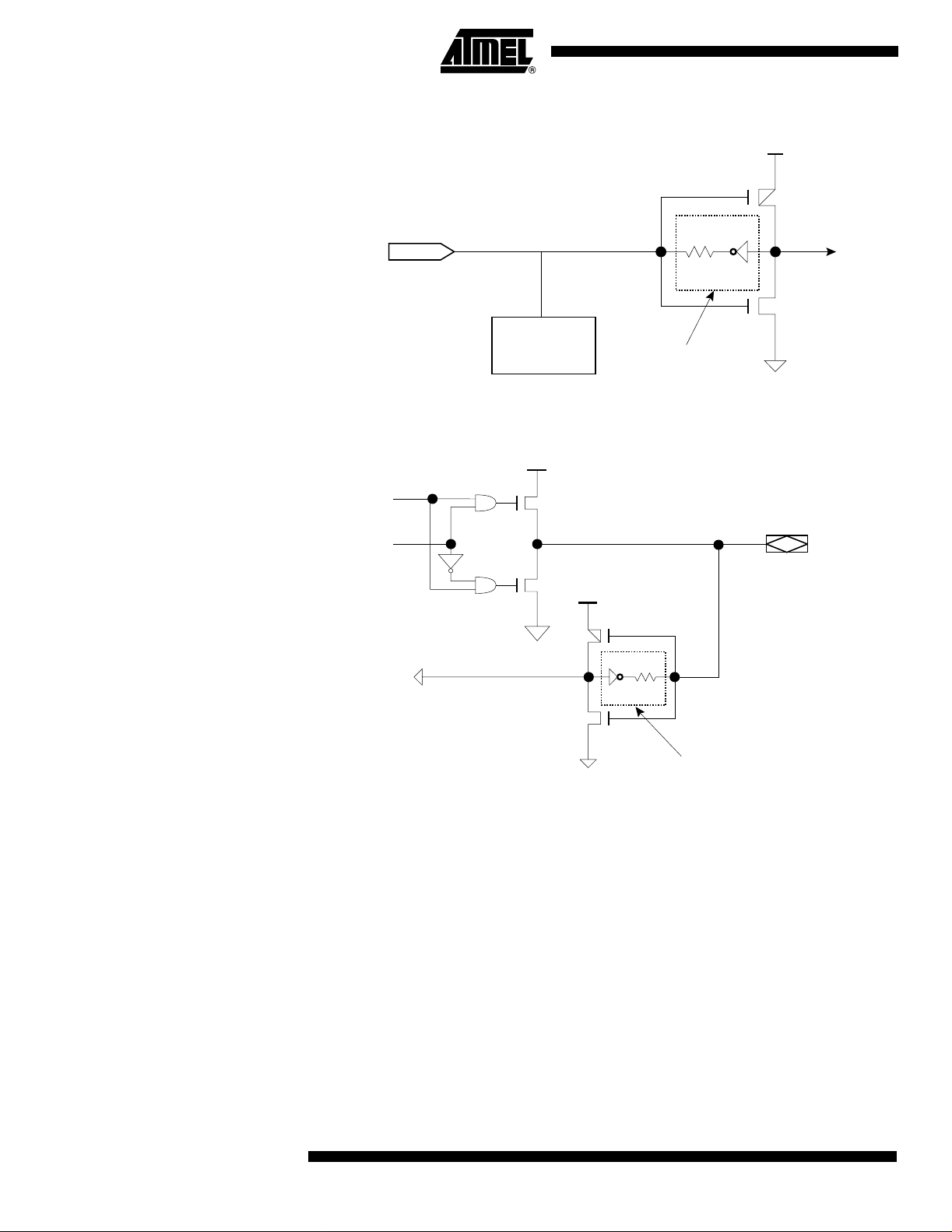
Input Diagram
V
CC
I/O Diagram
INPUT
DATA
OE
ESD
PROTECTION
CIRCUIT
V
CC
100K
PROGRAMMABLE
OPTION
I/O
V
CC
100K
Speed/Power Management
6
ATF1502ASV
PROGRAMMABLE
OPTION
The ATF1502ASV has several b uilt-in speed and power management features .
To further reduce power, eac h ATF1502ASV macrocell has a reduced-power bit feature.
To reduce power consumption this feature may be actived (by changing the default
value of OFF to ON) for any or all macrocells.
The ATF1502ASV also has an optional power-down mode. In this mode, current drops
to below 15 mA. When the power-down option is select ed, either PD 1 o r PD2 pins (or
both) can be used to power down the part. The power-down option is selected in the
design source file. When enabled, the device goes into power-down when either PD1 or
PD2 is high. In the power-down mode, all internal logic signals are latched and held, as
are any enabled outputs.
All pin transitions are ignored until the PD pin is brought low. When the power-down feature is enabled, the P D1 or PD2 pin cannot be used as a logic input or output. However,
the pin’s macrocell may still be used to generate buried foldback and cascade logic
signals.
1615G–PLD–09/02
Page 7

ATF1502ASV
All powe r-down AC cha racteristic parameters are computed from ext ernal inpu t or I/O
pins, with reduced-power bit turned on. F or macrocells in reduced-power mode
(reduced-power bit turned on), the reduced-power adder, t
parameters, which include the data paths t
LAD,tLAC,tIC,tACL,tACH
The ATF1502ASV macrocell also has an option whereby the power can be reduced on
a per-macrocell basis. By enabling this power-down option, macrocells that are not used
in an application can be turned down, thereby reducing the overall power consumption
of the device.
Each output also has i ndividual slew rate control. Thi s m ay be used to re duce system
noise by slowing down outputs that do not ne ed to op erate at m ax imu m speed. Outputs
default to slow switching, and may be specified as fast switching in the design file.
, must be added to the AC
RPA
and t
SEXP
.
Design Software Support
ATF1502ASV des igns are supported by several third-party tools. Automated fitters allow
logic synthesis using a variety of high-level description languages a nd formats.
Power-up Reset The ATF1502ASV is designed with a power-up reset, a feature critical for state machine
initialization. At a point delayed slightly from V
tialized, and the state of eac h o utput will depend on the polarity of its buffer. Howev er,
due to the asynchronous nature of reset and uncertainty of how V
system, the following conditions are required:
1. The V
rise must be m onotonic,
CC
2. After reset occurs, all input and feedback s et up times must be met before
driving the clock pin high, and,
3. The clock must remain stable during T
The ATF1502ASV has two options for the hysteresis about the reset level, V
and Large. To ensure a robust operating env ironment in applications where the dev ice
is operated near 3.0V, Atmel recommends that during the fitting p roce ss users configure
the device with the Power-up Reset hysteresis set to Large. For conversions, Atmel
POF2JED users should i nc lude the flag “-power_reset” on the command line after “filename.POF”. To allow the registers to be properly reinitial ized with the Large hysteresis
option selec ted, the following condition is added:
4.IfV
falls below 2.0V, it must shut off completely before the device is turned
CC
on again.
When t he Large hysteresis opt ion is act ive, I
amps as well.
crossing V
CC
.
D
is reduced by several hundred micro-
CC
, all registers will be ini-
RST
actually rises in the
CC
RST
,Small
Security Fuse Usage A single fuse is provided to prevent unaut horized copying of the ATF1502ASV fuse pat-
terns. Once programmed, fuse verify is inhibited. However, the 16-bit User Signature
remains accessible.
Programming ATF1502ASV devices are in-system programmable (ISP) devices utilizing the 4-pin
JTAG protocol. This capability eliminates package handling normally required for pro-
gramming and facilitates rapid design iterations and field changes.
Atmel provides ISP hardware and software to allow programming of the ATF1502ASV
via t he PC. ISP is performed by using either a download cable, a comparable board
tester or a simple microprocessor interface.
1615G–PLD–09/02
7
Page 8

When using the ISP hardware or software to program the ATF1502ASV devi ces, four
I/O pins mus t be reserv ed for the JTAG interface. However, the logic features that the
macroce lls have assoc iated with these I/O pins are still avai labl e to t he design for
burned logic functions.
To facilitate IS P programming by the Automated Test Equipment (ATE) vendors. Serial
Vector Format (SVF) files can be created by Atmel-provided software utilities.
ATF1502ASV devices can also be programmed using standard third-party programmers. W ith a third-par ty programmer, the JTAG I SP po rt can be di sab led, thereby
allowing four additional I/O pins to be used for logic.
Contact you r local Atmel representatives o r Atmel PLD applications f or details.
ISP Programming Protection
JTAG-BST/ISP Overview
The ATF 1502ASV has a spec ial feature that lock s the device and prevents the i nputs
and I/O from d rivin g if the programming p rocess is interrupted for any reason. The
inputs and I/O default to high-Z state during such a condition. In a ddition, the pin-keeper
option preserves the previous state of the input and I/O PMS during programming.
All A TF1502ASV devices are initially shipped in the erased state, thereby making them
ready to use for I SP.
Note: For more information refer to the “Designing for In-System Programmability with At mel
CPLDs” applicationnote.
The JTAG boundary-scan testing is c ont rolle d by the Test Ac c es s Port (TAP) controller
in the ATF1502 ASV. The boundary-scan technique involves the inclusion of a shift-register stage (contained in a boundary-scan cell) adjacent t o each component so that
signals at component boundaries can be controlled and observed using scan testing
methods. Each input pin and I/O pin has its own boundary-scan cell (BSC) to support
bounda ry -s c an testing. The ATF1502ASV does not inc lude a Test Reset (TRST) input
pin because the TAP controller is automatically reset at power-up. The five JTAG modes
supported include: SAMPLE/PRELOAD, EXTEST, BYPASS, IDCODE and HIGHZ.The
ATF1502ASV’s ISP can be fully described using JTAG’s BSDL as described in IEEE
Standard 1149.1b. This al lows ATF1502ASV programming to be described and implemented us ing any one of the third-party developm ent tools supporting this s t andard.
The ATF1502ASV has the option of using four JTAG-standard I/O pins for boundaryscan testing (BST) and in-system programming (ISP) purposes. The ATF1502AS V is
programmable t hrough the four JTAG pins using the I EEE standard JTAG programmi ng
protocol established by IEEE Standard 1149. 1 using 5V TTL -level programming signals
from the ISP interface for in-system programming. The JTAG feature is a programmable
option. If JTAG (BST or ISP) is not needed, the n the four JTAG control pins are av ailable as I/O pins.
JTAG Boundary-scan Cell (BSC) Testing
8
ATF1502ASV
The ATF1502ASV co ntains up to 32 I/O pins and four input pins, depending on the
device type and package type selected. Each input pin and I/O pin has its own boundary-scan cell (BSC) in order to support boundary-sc an testing as described in detail by
IEEE Standard 1149.1. A typical BSC consists of t hree capture registers or sca n registers and up to two update registers. There are two types of BSCs, one for input or I/O
pin, and one for the macroce ll s . The BSCs in the device are chained together through
the capture registers. Input to the capture register chain is fed in from the TDI pin while
the output is directed to the TDO pin. Capt ure registers are used to capture a ctive
device data signals, to shift data in and out of the device and to load data into t he update
registers. Control signals are generated internally by the JTAG TAP controller. The BSC
configuration for the input and I/O pins and macrocells is shown below.
1615G–PLD–09/02
Page 9

BSC Configuration
ATF1502ASV
for Input and I/O Pins
(Except JTAG TAP
Pins)
BSC Configuration
Dedicated
Input
To Internal
Logic
TDO
Capture
Registers
CLOCK
SHIFT
TDI
(From Next Register)
Note: The ATF1502ASV has a pull-up option on TMS and TDI pins. This feature is selected as
a design option.
for Macrocells
TDO
Q
OEJ
OUTJ
D
CLOCK
TDI
Shift
0
1
TDI
TDO
0
0
DQ
1
0
DQ
1
Capture
DR
Clock
DQ
DQ
Update
DR
1
0
1
Pin
Mode
1615G–PLD–09/02
BSC for I/O Pins and Macrocells
9
Page 10

Power-down Mode The ATF1502ASV includes an optional pin-controlled power-down feature. When this
mode is enabled, the PD pin acts as the power-down pi n. When the PD pin is high, the
device supply c urrent is reduced to less than 3 mA. During power-down, all output data
and internal logic states are latched and held. Therefore, all registered and combinatorial output data remain valid. Any outputs that were in a high-Z state at the onset will
remain at high-Z. During power-down, all input signals except the power-down pin are
blocked. Input and I/O hold latches remain active t o ensure that pins do not float to indeterminate levels, further reducing system power. The power-down pin feature is enabled
in the logic design file. Designs using the power-down pin may not use the PD pin l ogic
array input. Howeve r , all other PD pin macrocell resources may still be used, includin g
the buried feedback and foldback product term array inputs.
Power-down AC Characteristics
(1)(1)
Symbol Parameter
t
IVDH
t
GVDH
t
CVDH
t
DHIX
t
DHGX
t
DHCX
t
DLIV
t
DLGV
t
DLCV
t
DLOV
Notes: 1. For slow slew outputs, add t
Valid I, I/O before PD High 15 20 ns
Valid OE
Valid Clock
(1)
beforePD High 15 20 ns
(1)
before PD High 15 20 ns
I, I/O Don’t Care after PD High 25 30 ns
(1)
OE
Don’t Care after PD High 25 30 ns
(1)
Clock
Don’t Care after PD High 25 30 ns
PD Low t o Valid I, I/O 1 1 µs
PD Low t o Valid OE
PD Low t o Valid Clock
(1)
(1)
PD Low to Valid Output 1 1 µs
.
SSO
1. Pin or product term.
Absolute Maximum Ratings*
Temperature Under Bias.................................. -40°C to +85°C
Storage Temperature..................................... -65°C to +150°C
Voltage on Any Pin with
Respect to Ground .........................................-2.0V to +7.0V
Voltage on Input Pins
with Respect to Ground
During Programming.....................................-2.0V to +14.0V
ProgrammingVolt age with
Respect to Ground .......................................-2.0V to +14.0V
-15 -20
UnitsMin Max Min Max
11µs
11µs
*NOTICE: Stresses beyond those listed under “Absolute
Maximum Ratings” may cause permanent damage to the device. This is a stress rating only and
functionaloperation of the device at these or any
(1)
other conditions beyond those indicated in the
operational sections of this specification is not
implied. Exposure to absolute maximum rating
conditionsfor extendedperiodsmayaffect device
(1)
Note: 1. Minimum voltage is -0.6V DC, which may under-
reliability.
shoot to -2.0V for pulses of less than 20 ns.
(1)
which may overshoot to 7.0V for pulses of less
Maximum output pin voltageis V
+ 0.75V DC,
CC
than 20 ns.
10
ATF1502ASV
1615G–PLD–09/02
Page 11

ATF1502ASV
DC and AC Operating Conditions
Commercial Industrial
Operating Temperature (Ambient) 0°C-70°C-40°C-85°C
V
(3.3V) Power Supply 3.0V ± 3.6% 3.0V ± 3.6%
CC
DC Characteristics
Symbol Parameter Condition Min Typ Max Units
I
I
I
I
I
I
V
V
V
V
IL
IH
OZ
CC1
CC2
CC3
IL
IH
OL
OH
Input or I/O Low
Leakage Current
Input or I/O High
Leakage Current
Tri-state Output
Off-state Current
Power Supply Current, St andby
Power Supply Current,
Power-down Mode
(2)
Reduced-powerMode
Supply Current, Standby
Input Low Voltage -0.3 0.8 V
Input High Voltage 2.0 V
Output Low Voltage (TTL)
Output Low Voltage (CMOS)
Output High Voltage (TTL)
Output High Voltage (CMOS)
V
= V
IN
CC
-2 -10 µA
210
V
= VCCor GND-40 40 µA
O
= Max
V
CC
V
= 0, V
IN
VCC= Max
V
= 0, V
IN
VCC= Max
V
= 0, V
IN
= VIHor V
V
IN
Std Mode
CC
“PD” Mode 0.755.0mA
CC
Std Mode
CC
IL
VCC= MIN,IOL=8mA
= VIHor V
V
IN
IL
VCC= MIN,IOL= 0.1 mA
= VIHor V
V
IN
IL
VCC= MIN,IOH= 2.0 mA
= VIHor V
V
V
IN
CCIO
IL
= MIN,IOH= -0.1 mA
Com. 40mA
Ind. 45mA
Com. 25 mA
Ind. 30 mA
+ 0.3 V
CCINT
Com. 0.45V
Ind. 0.45
Com. 0.2 V
Ind. 0.2 V
2.4 V
-0.2
V
CCIO
Notes: 1. Not more than one output at a time should be shorted. Duration of short circuit test should not exceed 30 sec.
2. I
refers to the current in the reduced-power mode when macrocell reduced-power is turned on.
CC3
1615G–PLD–09/02
11
Page 12

Pin Capacitance
Typ Max Units Conditions
(1)
C
IN
C
I/O
8 10 pF VIN= 0V; f = 1.0 MHz
8 10 pF V
= 0V; f = 1.0 MHz
OUT
Note: 1. Typical values fornominal supply voltage. This parameter is only sampled and is not 100% tested. The OGI pin (high-voltage
pin during programming) has a maximum capacitance of 12 pF.
Timing Models
Internal Output
Enable Delay
t
IOE
Global Control
Input
Delay
t
IN
Switch
Matrix
t
UIM
Delay
t
GLOB
Logic Array
Delay
t
LAD
Register Control
Delay
t
LAC
t
IC
t
EN
FoldbackTerm
Delay
t
SEXP
Cascade Logic
Delay
t
PEXP
Fast Input
Delay
t
Register
Delay
t
SU
t
H
t
PRE
t
CLR
t
RD
t
COMB
t
FSU
t
FH
FIN
Output
Delay
t
OD1
t
OD2
t
OD3
t
XZ
t
ZX1
t
ZX2
t
ZX3
I/O
Delay
t
IO
Input Test Waveforms and Measurement Levels
tR,tF= 1.5 ns typical
Output AC T est Loads
3.0V
R1 = 703Ω
OUTPUT
PIN
CL=35pFR2 = 8060Ω
12
ATF1502ASV
1615G–PLD–09/02
Page 13

ATF1502ASV
AC Characteristics
Symbol Parameter
t
PD1
t
PD2
t
SU
t
H
t
FSU
t
FH
t
COP
t
CH
t
CL
t
ASU
t
AH
t
ACOP
t
ACH
t
ACL
t
CNT
f
CNT
t
ACNT
f
ACNT
f
MAX
t
IN
t
IO
t
FIN
t
SEXP
t
PEXP
t
LAD
t
LAC
t
IOE
t
OD1
t
ZX1
t
ZX2
Input or Feedback to Non-registered Output 3 15 20 ns
I/O Input or Feedbackto Non-registered Feedback 3 12 16 ns
Global Clock Setup Time 11 16 ns
Global Clock Hold Time 0 0 ns
Global Clock Setup Time of Fast Input 3 3 ns
Global Clock Hold Time of Fast Input 1 1.5 MHz
Global Clock to Output Delay 8 10 ns
Global Clock High Time 5 6 ns
Global Clock Low Time 5 6 ns
Array Clock Setup Time 44 ns
Array Clock Hold Time 4 5ns
Array Clock Output Delay 15 20 ns
Array Clock High Time 6 8 ns
Array Clock Low Time 6 8 ns
Minimum Clock Global Period 13 16 ns
Maximum Internal Global Clock Frequency 76.9 66 MHz
Minimum Array Clock Period 13 16 ns
Maximum Internal Array Clock Frequency 76.9 66 MHz
Maximum Clock Frequency 100 83.3 MHz
Input Pad and Buffer Delay 2 2 ns
I/O Input Pad and Buffer Delay 2 2 ns
Fast Input Delay 2 2 ns
Foldback Term Delay 8 10 ns
Cascade Logic Delay 1 1 ns
Logic Array Delay 6 7 ns
Logic Control Delay 6 7 ns
Internal Output Enable Delay 3 3 ns
Output Buffer and Pad Delay
(Slow slew rate = OFF;
V
= 3.3V; CL= 35 pF)
CC
Output Buffer Enable Delay
(Slow slew rate = OFF;
V
= 5.0V; CL= 35 pF)
CCIO
Output Buffer Enable Delay
(Slow slew rate = OFF;
V
= 3.3V; CL= 35 pF)
CCIO
(1)
-15 -20
UnitsMin Max Min Max
55ns
7 9ns
7 9ns
1615G–PLD–09/02
13
Page 14

AC Characteristics (Continued)
(1)
Symbol Parameter
Output Buffer Enable Delay
t
ZX3
t
XZ
t
SU
t
H
t
FSU
t
FH
t
RD
t
COMB
t
IC
t
EN
t
GLOB
t
PRE
t
CLR
t
UIM
t
RPA
(Slow slew rate = ON;
V
= 5.0V/3.3V; CL= 35 pF)
CCIO
Output Buffer Disable Delay (CL= 5pF) 6 7 ns
Register Setup Time 4 5ns
Register Hold Time 4 5ns
Register Setup Time of Fast I nput 2 2 ns
Register Hold Time of FastInput 2 2 ns
Register Delay 1 2 ns
Combinatorial Delay 1 2 ns
Array Clock Delay 6 7 ns
Register Enable Time 6 7 ns
Global Control Delay 1 1 ns
Register Preset Time 4 5ns
Register Clear Time 4 5ns
Switch Matrix Delay 2 2 ns
Reduced-power Adder
(2)
Note: 1. See ordering information for valid part numbers.
-15 -20
UnitsMin Max Min Max
10 11 ns
13 14 ns
14
ATF1502ASV
1615G–PLD–09/02
Page 15

ATF1502ASV
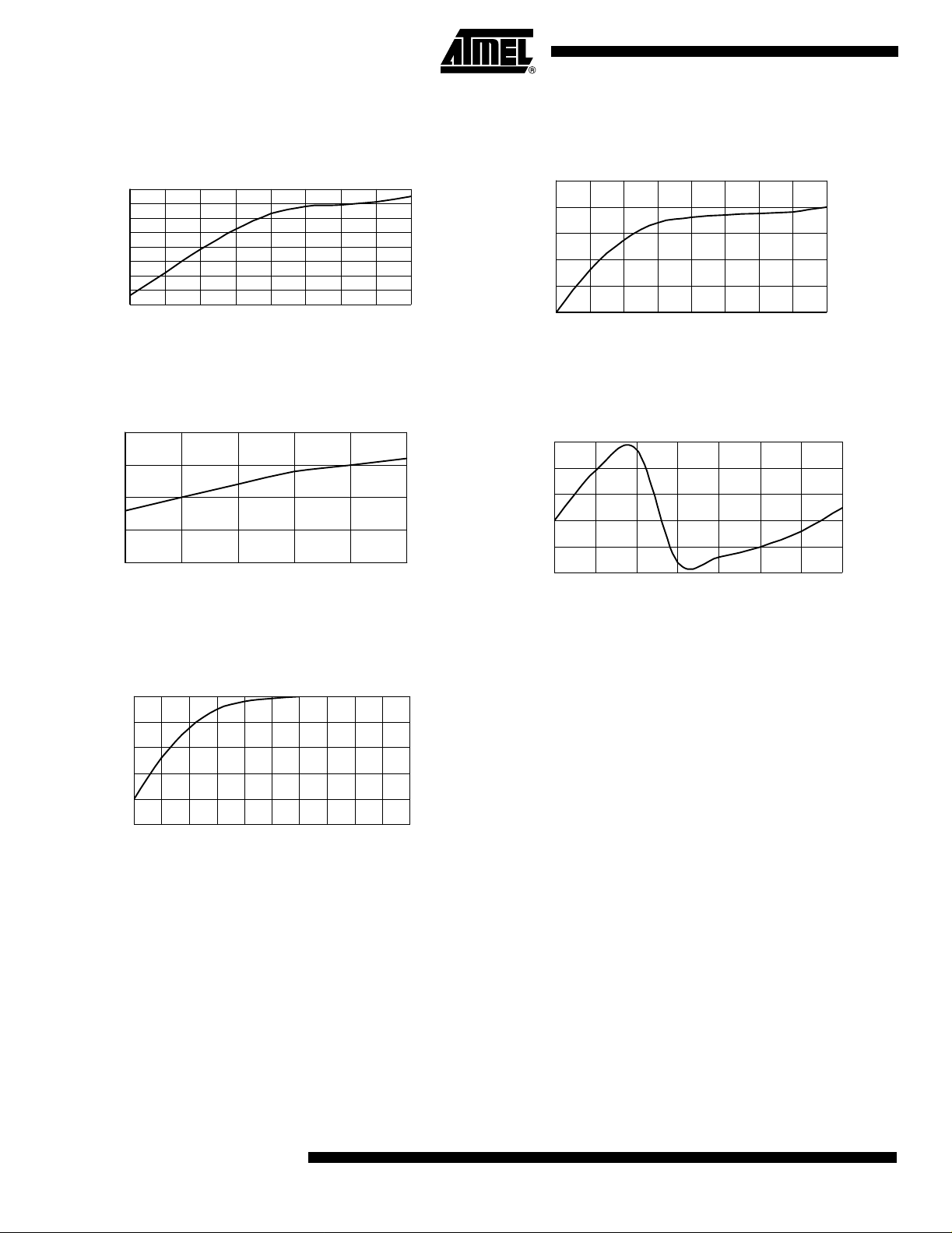
SUPPLY CURRENT VS. SUPPLY VOLTAGE
ASV VERSION(T
70
60
50
40
(mA)
CC
30
I
20
10
0
3 3.1 3.2 3.3 3.4 3.5 3.6
14
12
10
8
(mA)
CC
6
I
4
2
0
3 3.1 3.2 3.3 3.4 3.5 3.6
STANDARD POWER
SUPPLY CURRENT VS. SUPPLY VOLTAGE
PIN-CONTROLLED POWER-DOWN MODE (T
= 25°C, F = 0)
A
REDUCED POWER
(V)
V
CC
TBD
(V)
V
CC
=25°C,F=0)
A
OUTPUT SOURCE CURRENT VS. SUPPLY VOLTAGE
=2.4V,TA=25°C)
(V
OH
0
-2
-4
-6
(mA)
-8
OH
I
-10
-12
-14
-16
2.75 3.00 3.25 3.50 3.75 4.00
SUPPLY VOLTAGE (V)
SUPPLY CURRENT VS. SUPPLY VOLTAGE
(V)
= 25°C, F = 0)
A
ASVL (LOW-POWER)VERSION (T
5
4
3
(mA)
CC
I
2
1
0
3 3.1 3.2 3.3 3.4 3.5 3.6
TBD
V
CC
SUPPLY CURRENT VS. FREQUENCY
ASV VERSION (T
80.0
70.0
60.0
50.0
(mA)
40.0
CC
I
30.0
20.0
10.0
0.0
0.00 20.00 40.00 60.00 80.00 100.00
STANDARD POWER
FREQUENCY (MHz)
= 25°C)
A
REDUCED POWER
SUPPLY CURRENT VS. FREQUENCY
ASVL (LOW POWER) VERSION(T
80.0
70.0
60.0
50.0
(mA)
40.0
CC
I
30.0
20.0
10.0
0.0
0.00 5.00 10.00 15.00 20.00 25.00
STANDARD POWER
FREQUENCY (MHz)
= 25°C)
A
REDUCED POWER
1615G–PLD–09/02
15
Page 16
OUTPUT SOURCE CURRENT VS. OUTPUT VOLTAGE
=3.3V,TA=25°C)
(V
CC
10
0
-10
-20
(mA)
-30
OH
I
-40
-50
-60
-70
0.0 0.5 1.0 1.5 2.0 2.5 3.0 3.5 4.0
OUTPUT VOLTAGE (V)
OUTPUT SINKCURRENT VS. OUTPUT VOLTAGE
(V
=3.3V,TA= 25°C)
100
80
60
(mA)
OL
I
40
20
0
0 0.5 1 1.5 2 2.5 3 3.5 4
CC
OUTPUT VOLTAGE (V)
OUTPUT SINK CURRENT VS. SUPPLY VOLTAGE
=0.5V,TA=25°C)
(V
40
35
30
(mA)
OL
I
25
20
2.75 3.00 3.25 3.50 3.75 4.00
OL
SUPPLY V OLTAGE (V)
INPUT CLAMP CURRENT VS. INPUT VOLTAGE
(V
=3.3V,TA=25°C)
0
-20
-40
-60
-80
INPUT CURRENT (mA)
-100
-1 -0.9 -0.8 -0.7 -0.6 -0.5 -0.4 -0.3 -0.2 -0.1 0
CC
INPUT VOLTAGE(V)
INPUT CURRENT VS. INPUT VOLTAGE
(V
=3.3V,TA= 25°C)
15
10
5
0
INPUT CURRENT (uA)
-5
-10
00.511.522.533.5
CC
INPUT VOLTAGE (V)
16
ATF1502ASV
1615G–PLD–09/02
Page 17

ATF1502ASV Dedicated Pinouts
ATF1502ASV
44-lead
Dedicated Pin
INPUT/OE2/GCLK2 402
INPUT/GCLR 39 1
INPUT/OE1 3844
INPUT/GCLK13743
I/O / GCLK3 35 41
I/O / PD (1,2) 5, 19 11, 25
I/O / TDI (JTAG) 1 7
I/O / TMS (JTAG) 7 13
I/O / TCK (JTAG) 26 32
I/O/TDO(JTAG) 32 38
GND 4, 16, 24, 36 10, 22, 30, 42
V
CCI
# of Signal Pins 36 36
#User I/O Pins 32 32
TQFP
9, 17, 29, 41 3, 15, 23, 35
44-lead
J-lead
OE (1, 2) Global OE pins
GCLR Global Clear pin
GCLK (1, 2, 3) Global Clock pins
PD (1, 2) Power-down pins
TDI, TMS, TCK,TDO JTAG pins used for boundary-scan t esting or in-system programming
GND Ground pins
V
CCI
VCC pins for the device (+3.3V)
1615G–PLD–09/02
17
Page 18

ATF1502ASV I/O Pinouts
MC PLC 44-lead PLCC 44-lead TQFP
1A442
2A543
3A644
4/TDI A 7 1
5A8 2
6A93
7/PD1 A115
8 A126
9/TMS A137
10 A 148
11 A 16 10
12 A 17 11
13 A 18 12
14 A1913
15 A 20 14
16 A 21 15
17B4135
18B4034
19 B 39 33
20/TDO B 38 32
21 B 37 31
22 B 36 30
23 B 34 28
24B33 27
25/TCK B 32 26
26 B 31 25
27B29 23
28B28 22
29 B 27 21
30 B 26 20
31/PD2 B 25 19
32 B 24 18
18
ATF1502ASV
1615G–PLD–09/02
Page 19

ATF1502ASV
Ordering Information
t
PD
(ns)
15 8 100 ATF1502ASV-15 AC44
15 8 100 ATF1502ASV-15 AI44
20 12 83.3 ATF1502ASV-20 AC44
20 12 83.3 ATF1502ASV-20 AI44
Note: 1. Shaded area indicates preliminary data.
t
CO1
(ns)
Using “C” Product for Industrial
There is very little risk in using “C” devic es for industrial applications because the VCCconditions for 3.3V products are
the same for commercial and industrial (there is only 15°C difference at the high end of the temperature range). To us e
commercial product for industrial temperature ranges, de-rate I
f
MAX
(MHz) Ordering Code Package Operation Range
ATF1502ASV-15 JC44
ATF1502ASV-15 JI44
ATF1502ASV-20 JC44
ATF1502ASV-20 JI44
by 15%.
CC
44A
44J
44A
44J
44A
44J
44A
44J
Commercial
(0°Cto70°C)
Industrial
(-40°Cto+85°C)
Commercial
(0°Cto70°C)
Industrial
(-40°Cto+85°C)
Package Type
44A 44-lead, Thin Plastic Gull Wing Quad Fl atpack (TQFP)
44J 44-lead, Plastic J-leaded Chip Carrier OTP (PLCC)
1615G–PLD–09/02
19
Page 20

Packaging Information
44A – TQFP
PIN 1
B
PIN 1 IDENTIFIER
e
E1 E
D1
D
C
0˚~7˚
A1
L
Notes: 1. This package conforms to JEDEC reference MS-026, Variation ACB.
2. Dimensions D1 and E1 do not include mold protrusion. Allowable
protrusion is 0.25 mm per side. Dimensions D1 and E1 are maximum
plastic body size dimensions including mold mismatch.
3. Lead coplanarity is 0.10 mm maximum.
A2 A
SYMBOL
COMMON DIMENSIONS
(Unit of Measure = mm)
MIN
A – – 1.20
A1 0.05 – 0.15
A2 0.95 1.00 1.05
D 11.75 12.00 12.25
D1 9.90 10.00 10.10 Note 2
E 11.75 12.00 12.25
E1 9.90 10.00 10.10 Note 2
B 0.30 – 0.45
C 0.09 – 0.20
L 0.45 – 0.75
e 0.80 TYP
NOM
MAX
NOTE
20
2325 Orchard Parkway
R
San Jose, CA 95131
ATF1502ASV
TITLE
44A, 44-lead, 10 x 10 mm Body Size, 1.0 mm Body Thickness,
0.8 mm Lead Pitch, Thin Profile Plastic Quad Flat Package (TQFP)
10/5/2001
DRAWING NO.
44A
1615G–PLD–09/02
REV.
B
Page 21

44J–PLCC
ATF1502ASV
1.14(0.045) X 45°
B
e
0.51(0.020)MAX
45° MAX (3X)
Notes: 1. This package conforms to JEDEC reference MS-018, Variation AC.
2. Dimensions D1 and E1 do not include mold protrusion.
Allowable protrusion is .010"(0.254 mm) per side. Dimension D1
and E1 include mold mismatch and are measured at the extreme
material condition at the upper or lower parting line.
3. Lead coplanarity is 0.004" (0.102 mm) maximum.
PIN NO. 1
IDENTIFIER
D1
D
1.14(0.045) X 45°
E1 E
0.318(0.0125)
0.191(0.0075)
NOM
D2/E2
MAX
B1
A2
A1
A
COMMON DIMENSIONS
(Unit of Measure = mm)
SYMBOL
A 4.191 – 4.572
A1 2.286 – 3.048
A2 0.508 – –
D 17.399 – 17.653
D1 16.510 – 16.662 Note 2
E 17.399 – 17.653
E1 16.510 – 16.662 Note 2
D2/E2 14.986 – 16.002
B 0.660 – 0.813
B1 0.330 – 0.533
e 1.270 TYP
MIN
NOTE
R
1615G–PLD–09/02
2325 Orchard Parkway
San Jose, CA 95131
TITLE
44J, 44-lead, Plastic J-leaded Chip Carrier (PLCC)
DRAWING NO.
44J
10/04/01
REV.
B
21
Page 22

Atmel Headquarters Atmel Operations
Corporate Headquarters
2325 O rchard Park way
San Jose, CA 95131
TEL 1( 408) 441-03 11
FAX 1(408) 487-2600
Europe
Atmel Sarl
Route des Ar senau x 41
Case P ostale 80
CH-1705 Fribourg
Switzerland
TEL ( 41) 2 6-426-5555
FAX (41) 26-426-5500
Asia
Room 1219
Chinachem Golden Plaza
77 Mod y Road Tsimshatsu i
East Kowloon
Hong Kong
TEL ( 852) 2721-9778
FAX (852) 2722-1369
Japan
9F, T onets u Shinkawa Bl dg.
1-24-8 Shinkaw a
Chuo-ku, Tokyo 104-00 33
Japan
TEL ( 81) 3 -3523- 3551
FAX (81) 3-3523-7581
Memory
2325 O rch ard Parkway
San Jose, CA 95131
TEL 1(408) 441-0311
FAX 1(408) 436 -4314
Microcontrollers
2325 O rch ard Parkway
San Jose, CA 95131
TEL 1(408) 441-0311
FAX 1(408) 436 -4314
La Ch antr erie
BP 70602
44306 Nant es Cedex 3, Fra nce
TEL (33) 2-40-18-18-18
FAX (3 3) 2-40-18-1 9-60
ASIC/ASSP/Smart Cards
Zone Indus trielle
13106 Rousset Cedex, France
TEL (33) 4-42-53-60-00
FAX (33) 4-42-53-60-01
1150 E ast Cheyenn e Mtn. Blvd.
Colorado Springs, C O 8090 6
TEL 1(719) 5 76-3300
FAX 1(719 ) 540-1759
Scottish Enterpris e Technology Park
Maxwell Building
East Kilbride G750QR, Scotlan d
TEL (44) 1355-803-000
FAX (44) 1355- 242-743
RF/Automotive
Theresienstrasse 2
Postfach 3535
74025 Heilbronn, Germany
TEL ( 49) 71-31-6 7-0
FAX (49) 71-31-67-2340
1150 East Cheyenne Mtn. Blvd .
Colorado Spring s, CO 80906
TEL 1( 719) 576-3300
FAX 1(719) 540-1759
Biometrics/Imaging/Hi-Rel MPU/
High Speed Converters/RF Datacom
Avenue de R ocheplei ne
BP 123
38521 S aint- Egreve Cedex, France
TEL ( 33) 4-76- 58-30-00
FAX (33) 4-76-58-34-80
e-mail
literature@atmel.com
Web Site
http://www.atmel.com
© Atmel Corpor ation 2002.
Atmel Corporation makes no warranty for the use of its products, other than those expr essly contained in the Company’s standard warranty
which is detailed in A tmel’s Te rms and Condi tions locat ed on the Com pany’s w eb si te. The Co mpany assumes no r es ponsibility for any errors
which may app ear in this document, r es erves the right to cha nge devices or spec if i cation s detailed herein at any time w i t h out notice, and doe s
not make any commitment to up date t he inform ation contain ed herein . No li ce ns es to p atents or other intellectua l proper t y of Atmel are gr a nted
by the Comp any in connec tion with t he sale of Atm el products, expres s ly or by implication . At m el’s produc ts a r e n ot a uthori zed for use as cr itical
components in life support devices or systems.
ATMEL®is the registered trademark of Atmel.
Other t erms and pro du ct names may be the tradem arks of others.
Printed onrecycledpaper .
1615G–PLD–09/02 xM
 Loading...